EP1865563A2 - Processus pour galvaniser à l'aide de lumière - Google Patents
Processus pour galvaniser à l'aide de lumière Download PDFInfo
- Publication number
- EP1865563A2 EP1865563A2 EP07010932A EP07010932A EP1865563A2 EP 1865563 A2 EP1865563 A2 EP 1865563A2 EP 07010932 A EP07010932 A EP 07010932A EP 07010932 A EP07010932 A EP 07010932A EP 1865563 A2 EP1865563 A2 EP 1865563A2
- Authority
- EP
- European Patent Office
- Prior art keywords
- wafer
- metal
- plating
- silver
- bath
- Prior art date
- Legal status (The legal status is an assumption and is not a legal conclusion. Google has not performed a legal analysis and makes no representation as to the accuracy of the status listed.)
- Withdrawn
Links
Images

Classifications
-
- C—CHEMISTRY; METALLURGY
- C25—ELECTROLYTIC OR ELECTROPHORETIC PROCESSES; APPARATUS THEREFOR
- C25D—PROCESSES FOR THE ELECTROLYTIC OR ELECTROPHORETIC PRODUCTION OF COATINGS; ELECTROFORMING; APPARATUS THEREFOR
- C25D7/00—Electroplating characterised by the article coated
- C25D7/12—Semiconductors
- C25D7/123—Semiconductors first coated with a seed layer or a conductive layer
- C25D7/126—Semiconductors first coated with a seed layer or a conductive layer for solar cells
-
- C—CHEMISTRY; METALLURGY
- C23—COATING METALLIC MATERIAL; COATING MATERIAL WITH METALLIC MATERIAL; CHEMICAL SURFACE TREATMENT; DIFFUSION TREATMENT OF METALLIC MATERIAL; COATING BY VACUUM EVAPORATION, BY SPUTTERING, BY ION IMPLANTATION OR BY CHEMICAL VAPOUR DEPOSITION, IN GENERAL; INHIBITING CORROSION OF METALLIC MATERIAL OR INCRUSTATION IN GENERAL
- C23C—COATING METALLIC MATERIAL; COATING MATERIAL WITH METALLIC MATERIAL; SURFACE TREATMENT OF METALLIC MATERIAL BY DIFFUSION INTO THE SURFACE, BY CHEMICAL CONVERSION OR SUBSTITUTION; COATING BY VACUUM EVAPORATION, BY SPUTTERING, BY ION IMPLANTATION OR BY CHEMICAL VAPOUR DEPOSITION, IN GENERAL
- C23C18/00—Chemical coating by decomposition of either liquid compounds or solutions of the coating forming compounds, without leaving reaction products of surface material in the coating; Contact plating
- C23C18/16—Chemical coating by decomposition of either liquid compounds or solutions of the coating forming compounds, without leaving reaction products of surface material in the coating; Contact plating by reduction or substitution, e.g. electroless plating
- C23C18/1601—Process or apparatus
- C23C18/1603—Process or apparatus coating on selected surface areas
- C23C18/1605—Process or apparatus coating on selected surface areas by masking
-
- C—CHEMISTRY; METALLURGY
- C23—COATING METALLIC MATERIAL; COATING MATERIAL WITH METALLIC MATERIAL; CHEMICAL SURFACE TREATMENT; DIFFUSION TREATMENT OF METALLIC MATERIAL; COATING BY VACUUM EVAPORATION, BY SPUTTERING, BY ION IMPLANTATION OR BY CHEMICAL VAPOUR DEPOSITION, IN GENERAL; INHIBITING CORROSION OF METALLIC MATERIAL OR INCRUSTATION IN GENERAL
- C23C—COATING METALLIC MATERIAL; COATING MATERIAL WITH METALLIC MATERIAL; SURFACE TREATMENT OF METALLIC MATERIAL BY DIFFUSION INTO THE SURFACE, BY CHEMICAL CONVERSION OR SUBSTITUTION; COATING BY VACUUM EVAPORATION, BY SPUTTERING, BY ION IMPLANTATION OR BY CHEMICAL VAPOUR DEPOSITION, IN GENERAL
- C23C18/00—Chemical coating by decomposition of either liquid compounds or solutions of the coating forming compounds, without leaving reaction products of surface material in the coating; Contact plating
- C23C18/16—Chemical coating by decomposition of either liquid compounds or solutions of the coating forming compounds, without leaving reaction products of surface material in the coating; Contact plating by reduction or substitution, e.g. electroless plating
- C23C18/1601—Process or apparatus
- C23C18/1603—Process or apparatus coating on selected surface areas
- C23C18/1607—Process or apparatus coating on selected surface areas by direct patterning
- C23C18/1608—Process or apparatus coating on selected surface areas by direct patterning from pretreatment step, i.e. selective pre-treatment
-
- C—CHEMISTRY; METALLURGY
- C23—COATING METALLIC MATERIAL; COATING MATERIAL WITH METALLIC MATERIAL; CHEMICAL SURFACE TREATMENT; DIFFUSION TREATMENT OF METALLIC MATERIAL; COATING BY VACUUM EVAPORATION, BY SPUTTERING, BY ION IMPLANTATION OR BY CHEMICAL VAPOUR DEPOSITION, IN GENERAL; INHIBITING CORROSION OF METALLIC MATERIAL OR INCRUSTATION IN GENERAL
- C23C—COATING METALLIC MATERIAL; COATING MATERIAL WITH METALLIC MATERIAL; SURFACE TREATMENT OF METALLIC MATERIAL BY DIFFUSION INTO THE SURFACE, BY CHEMICAL CONVERSION OR SUBSTITUTION; COATING BY VACUUM EVAPORATION, BY SPUTTERING, BY ION IMPLANTATION OR BY CHEMICAL VAPOUR DEPOSITION, IN GENERAL
- C23C18/00—Chemical coating by decomposition of either liquid compounds or solutions of the coating forming compounds, without leaving reaction products of surface material in the coating; Contact plating
- C23C18/16—Chemical coating by decomposition of either liquid compounds or solutions of the coating forming compounds, without leaving reaction products of surface material in the coating; Contact plating by reduction or substitution, e.g. electroless plating
- C23C18/1601—Process or apparatus
- C23C18/1603—Process or apparatus coating on selected surface areas
- C23C18/1614—Process or apparatus coating on selected surface areas plating on one side
-
- C—CHEMISTRY; METALLURGY
- C23—COATING METALLIC MATERIAL; COATING MATERIAL WITH METALLIC MATERIAL; CHEMICAL SURFACE TREATMENT; DIFFUSION TREATMENT OF METALLIC MATERIAL; COATING BY VACUUM EVAPORATION, BY SPUTTERING, BY ION IMPLANTATION OR BY CHEMICAL VAPOUR DEPOSITION, IN GENERAL; INHIBITING CORROSION OF METALLIC MATERIAL OR INCRUSTATION IN GENERAL
- C23C—COATING METALLIC MATERIAL; COATING MATERIAL WITH METALLIC MATERIAL; SURFACE TREATMENT OF METALLIC MATERIAL BY DIFFUSION INTO THE SURFACE, BY CHEMICAL CONVERSION OR SUBSTITUTION; COATING BY VACUUM EVAPORATION, BY SPUTTERING, BY ION IMPLANTATION OR BY CHEMICAL VAPOUR DEPOSITION, IN GENERAL
- C23C18/00—Chemical coating by decomposition of either liquid compounds or solutions of the coating forming compounds, without leaving reaction products of surface material in the coating; Contact plating
- C23C18/16—Chemical coating by decomposition of either liquid compounds or solutions of the coating forming compounds, without leaving reaction products of surface material in the coating; Contact plating by reduction or substitution, e.g. electroless plating
- C23C18/1601—Process or apparatus
- C23C18/1633—Process of electroless plating
- C23C18/1635—Composition of the substrate
- C23C18/1639—Substrates other than metallic, e.g. inorganic or organic or non-conductive
- C23C18/1642—Substrates other than metallic, e.g. inorganic or organic or non-conductive semiconductor
-
- C—CHEMISTRY; METALLURGY
- C23—COATING METALLIC MATERIAL; COATING MATERIAL WITH METALLIC MATERIAL; CHEMICAL SURFACE TREATMENT; DIFFUSION TREATMENT OF METALLIC MATERIAL; COATING BY VACUUM EVAPORATION, BY SPUTTERING, BY ION IMPLANTATION OR BY CHEMICAL VAPOUR DEPOSITION, IN GENERAL; INHIBITING CORROSION OF METALLIC MATERIAL OR INCRUSTATION IN GENERAL
- C23C—COATING METALLIC MATERIAL; COATING MATERIAL WITH METALLIC MATERIAL; SURFACE TREATMENT OF METALLIC MATERIAL BY DIFFUSION INTO THE SURFACE, BY CHEMICAL CONVERSION OR SUBSTITUTION; COATING BY VACUUM EVAPORATION, BY SPUTTERING, BY ION IMPLANTATION OR BY CHEMICAL VAPOUR DEPOSITION, IN GENERAL
- C23C18/00—Chemical coating by decomposition of either liquid compounds or solutions of the coating forming compounds, without leaving reaction products of surface material in the coating; Contact plating
- C23C18/16—Chemical coating by decomposition of either liquid compounds or solutions of the coating forming compounds, without leaving reaction products of surface material in the coating; Contact plating by reduction or substitution, e.g. electroless plating
- C23C18/1601—Process or apparatus
- C23C18/1633—Process of electroless plating
- C23C18/1646—Characteristics of the product obtained
- C23C18/165—Multilayered product
-
- C—CHEMISTRY; METALLURGY
- C23—COATING METALLIC MATERIAL; COATING MATERIAL WITH METALLIC MATERIAL; CHEMICAL SURFACE TREATMENT; DIFFUSION TREATMENT OF METALLIC MATERIAL; COATING BY VACUUM EVAPORATION, BY SPUTTERING, BY ION IMPLANTATION OR BY CHEMICAL VAPOUR DEPOSITION, IN GENERAL; INHIBITING CORROSION OF METALLIC MATERIAL OR INCRUSTATION IN GENERAL
- C23C—COATING METALLIC MATERIAL; COATING MATERIAL WITH METALLIC MATERIAL; SURFACE TREATMENT OF METALLIC MATERIAL BY DIFFUSION INTO THE SURFACE, BY CHEMICAL CONVERSION OR SUBSTITUTION; COATING BY VACUUM EVAPORATION, BY SPUTTERING, BY ION IMPLANTATION OR BY CHEMICAL VAPOUR DEPOSITION, IN GENERAL
- C23C18/00—Chemical coating by decomposition of either liquid compounds or solutions of the coating forming compounds, without leaving reaction products of surface material in the coating; Contact plating
- C23C18/16—Chemical coating by decomposition of either liquid compounds or solutions of the coating forming compounds, without leaving reaction products of surface material in the coating; Contact plating by reduction or substitution, e.g. electroless plating
- C23C18/31—Coating with metals
- C23C18/38—Coating with copper
-
- C—CHEMISTRY; METALLURGY
- C25—ELECTROLYTIC OR ELECTROPHORETIC PROCESSES; APPARATUS THEREFOR
- C25D—PROCESSES FOR THE ELECTROLYTIC OR ELECTROPHORETIC PRODUCTION OF COATINGS; ELECTROFORMING; APPARATUS THEREFOR
- C25D5/00—Electroplating characterised by the process; Pretreatment or after-treatment of workpieces
- C25D5/011—Electroplating using electromagnetic wave irradiation
-
- H—ELECTRICITY
- H10—SEMICONDUCTOR DEVICES; ELECTRIC SOLID-STATE DEVICES NOT OTHERWISE PROVIDED FOR
- H10F—INORGANIC SEMICONDUCTOR DEVICES SENSITIVE TO INFRARED RADIATION, LIGHT, ELECTROMAGNETIC RADIATION OF SHORTER WAVELENGTH OR CORPUSCULAR RADIATION
- H10F77/00—Constructional details of devices covered by this subclass
- H10F77/20—Electrodes
- H10F77/206—Electrodes for devices having potential barriers
- H10F77/211—Electrodes for devices having potential barriers for photovoltaic cells
-
- C—CHEMISTRY; METALLURGY
- C23—COATING METALLIC MATERIAL; COATING MATERIAL WITH METALLIC MATERIAL; CHEMICAL SURFACE TREATMENT; DIFFUSION TREATMENT OF METALLIC MATERIAL; COATING BY VACUUM EVAPORATION, BY SPUTTERING, BY ION IMPLANTATION OR BY CHEMICAL VAPOUR DEPOSITION, IN GENERAL; INHIBITING CORROSION OF METALLIC MATERIAL OR INCRUSTATION IN GENERAL
- C23C—COATING METALLIC MATERIAL; COATING MATERIAL WITH METALLIC MATERIAL; SURFACE TREATMENT OF METALLIC MATERIAL BY DIFFUSION INTO THE SURFACE, BY CHEMICAL CONVERSION OR SUBSTITUTION; COATING BY VACUUM EVAPORATION, BY SPUTTERING, BY ION IMPLANTATION OR BY CHEMICAL VAPOUR DEPOSITION, IN GENERAL
- C23C18/00—Chemical coating by decomposition of either liquid compounds or solutions of the coating forming compounds, without leaving reaction products of surface material in the coating; Contact plating
- C23C18/16—Chemical coating by decomposition of either liquid compounds or solutions of the coating forming compounds, without leaving reaction products of surface material in the coating; Contact plating by reduction or substitution, e.g. electroless plating
- C23C18/1601—Process or apparatus
- C23C18/1633—Process of electroless plating
- C23C18/1655—Process features
- C23C18/1664—Process features with additional means during the plating process
- C23C18/1667—Radiant energy, e.g. laser
-
- C—CHEMISTRY; METALLURGY
- C23—COATING METALLIC MATERIAL; COATING MATERIAL WITH METALLIC MATERIAL; CHEMICAL SURFACE TREATMENT; DIFFUSION TREATMENT OF METALLIC MATERIAL; COATING BY VACUUM EVAPORATION, BY SPUTTERING, BY ION IMPLANTATION OR BY CHEMICAL VAPOUR DEPOSITION, IN GENERAL; INHIBITING CORROSION OF METALLIC MATERIAL OR INCRUSTATION IN GENERAL
- C23C—COATING METALLIC MATERIAL; COATING MATERIAL WITH METALLIC MATERIAL; SURFACE TREATMENT OF METALLIC MATERIAL BY DIFFUSION INTO THE SURFACE, BY CHEMICAL CONVERSION OR SUBSTITUTION; COATING BY VACUUM EVAPORATION, BY SPUTTERING, BY ION IMPLANTATION OR BY CHEMICAL VAPOUR DEPOSITION, IN GENERAL
- C23C18/00—Chemical coating by decomposition of either liquid compounds or solutions of the coating forming compounds, without leaving reaction products of surface material in the coating; Contact plating
- C23C18/16—Chemical coating by decomposition of either liquid compounds or solutions of the coating forming compounds, without leaving reaction products of surface material in the coating; Contact plating by reduction or substitution, e.g. electroless plating
- C23C18/31—Coating with metals
- C23C18/42—Coating with noble metals
-
- C—CHEMISTRY; METALLURGY
- C25—ELECTROLYTIC OR ELECTROPHORETIC PROCESSES; APPARATUS THEREFOR
- C25D—PROCESSES FOR THE ELECTROLYTIC OR ELECTROPHORETIC PRODUCTION OF COATINGS; ELECTROFORMING; APPARATUS THEREFOR
- C25D3/00—Electroplating: Baths therefor
- C25D3/02—Electroplating: Baths therefor from solutions
- C25D3/46—Electroplating: Baths therefor from solutions of silver
-
- Y—GENERAL TAGGING OF NEW TECHNOLOGICAL DEVELOPMENTS; GENERAL TAGGING OF CROSS-SECTIONAL TECHNOLOGIES SPANNING OVER SEVERAL SECTIONS OF THE IPC; TECHNICAL SUBJECTS COVERED BY FORMER USPC CROSS-REFERENCE ART COLLECTIONS [XRACs] AND DIGESTS
- Y02—TECHNOLOGIES OR APPLICATIONS FOR MITIGATION OR ADAPTATION AGAINST CLIMATE CHANGE
- Y02E—REDUCTION OF GREENHOUSE GAS [GHG] EMISSIONS, RELATED TO ENERGY GENERATION, TRANSMISSION OR DISTRIBUTION
- Y02E10/00—Energy generation through renewable energy sources
- Y02E10/50—Photovoltaic [PV] energy
Definitions
- the present invention relates generally to the field of metal plating. More particularly, the present invention relates to the field of metal plating of photovoltaic devices.
- Photovoltaic devices such as solar cells, often include a semiconductor wafer which forms a single large PN junction. Electromagnetic radiation such as sunlight incident upon that junction produces electrical carriers in the device and generates an electrical current, which must be collected and conveyed to an external circuit. The generated current is roughly proportional to the incident radiation.
- Metallic patterns which are in ohmic contact with the two sides of the PN junction collect the current. Such metallic patterns need to provide a low resistance path to minimize resistive losses of the generated current.
- the metallic pattern must be limited in its physical extent, especially on the front surface of the device, so as to minimize surface area that is blocks incident radiant energy, i.e. energy lost for current generation purposes.
- the front metallic pattern includes narrow strips of very highly conductive material.
- a satisfactory metal pattern can be achieved by applying a thin patterned layer of an ohmic contact and barrier layer material and by subsequent metallization.
- One metallization approach is screen-printed silver paste, which provides a thick conductor of low enough resistance for many applications.
- the silver paste itself is not of low enough resistance to provide optimum solar cell performance.
- a more conductive material such as plated silver or copper is needed to minimize resistive losses which lower the solar cell efficiency.
- Silver has been deposited electrolytically onto a photovoltaic device, where current has been generated in the device itself through the use of radiant energy. In such electrolytic silver plating process, uniform deposition of the silver layer is achieved when a voltage is applied to one surface of the device while simultaneously illuminating the opposite surface of the device with radiant energy.
- the present invention provides a method of plating an electrical contact on a light-sensitive device displaying a photovoltaic effect (a "photovoltaic device"), including providing a semiconductive wafer having at least two major surfaces, the wafer having a photovoltaic junction formed therein so that when one of the major surfaces of the wafer is exposed to light, negative charges collect at a first of the major surfaces and positive charges collect at a second of the major surfaces, contacting the wafer with a cyanide-free metal plating bath, applying a potential to the plating bath and exposing the wafer to light to deposit a layer of metal onto the first major surface, wherein the plating bath is an aqueous solution and includes metal ions, at least one water-soluble nitro-containing compound, at least one surfactant, at least one amido-compound, and at least one component chosen from a water-soluble amino acid, a water-soluble sulfonic acid, and mixtures thereof.
- a photovoltaic device a photovoltaic device
- a coating of a metal on the second major surface is provided prior to contacting wafer with the cyanide-free metal plating bath. In this embodiment, migration of the metal from the coating on the second major surface into the plating bath and thence to the negatively charged first major surface occurs.
- the cyanide-free metal plating baths used in the present invention have sufficient stability under the conditions of illumination used in light assisted electroplating to provide metal deposits on photovoltaic devices that meet desired specifications.
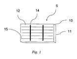
- Fig. 1 illustrates a photovoltaic device of the invention.
- Fig. 2 is a schematic representation of providing a metal coating on a photovoltaic device according to the invention.
- plating refers to the deposition of a metal layer, such as by electroplating or electroless plating, as the context indicates.
- Deposition and “plating” are used interchangeably throughout this specification.
- photovoltaic devices may be used in the present invention, such as, for example, solar cells.
- photovoltaic devices are typically produced using a semiconductor substrate, such as a semiconductor wafer.
- solar cells are composed of monocrystalline or polycrystalline or amorphous silicon wafers.
- solar cells are composed of polycrystalline silicon wafers. While the description below is with regard to silicon wafers, it will be appreciated by those skilled in the art that other suitable semiconductor wafers, such as gallium-arsenide, silicon-germanium, and germanium, may suitably be used with the present invention.
- silicon wafers When silicon wafers are used, they typically have a p-type base doping.
- the wafers may be circular, square or rectangular in shape or may be any other suitable shape. Such wafers may have a wide variety of dimensions. For example, circular wafers may have a diameter of 150 nm, 200 nm, 300 nm, 400 nm, or greater.
- the rear side of a wafer is metallized.
- the entire rear side may be metal coated or a portion of the rear side may be metal coated, such as to form a grid.
- Such rear side metallization may be provided by a variety of techniques, and may be done prior to the metallization of the front side of the wafer or may be done simultaneously with the metallization of the front side of the wafer.
- a metal coating is applied to the rear side in the form of an electrically conductive paste, such as a silver-containing paste, an aluminum-containing paste or a silver and aluminum-containing paste.
- Such conductive pastes typically include conductive particles embedded in a glass matrix and an organic binder. Conductive pastes may be applied to the wafer by a variety of techniques, such as screen printing.
- the paste After the paste is applied, it is fired to remove the organic binder.
- a conductive paste containing aluminum When a conductive paste containing aluminum is used, the aluminum partially diffuses into the rear side of the wafer, or if used in a paste also containing silver, may alloy with the silver.
- Use of such aluminum-containing paste may improve the resistive contact and provide a "p+"-doped region. Heavily doped "p+"-type regions by previous application of aluminum or boron with subsequent interdiffusion may also be produced.
- an aluminum-containing paste may be applied to the rear side and fired before the application of the rear side metal coating. The residue from the fired aluminum-containing paste may optionally be removed prior to the application of the rear side metal coating.
- a seed layer may be deposited on the rear side of the wafer and a metal coating may be deposited on the seed layer by electroless or electrolytic plating.
- Such metal deposition on the seed layer on the rear side of the wafer may be performed simultaneously with the metal deposition on the front side of the wafer using the present invention.
- the front side of the wafer may optionally be subjected to crystal-oriented texture etching in order to impart to the surface an improved light incidence geometry which reduces reflections.
- phosphorus diffusion or ion implantation takes place on the front side of the wafer to produce an n-doped region and providing the wafer with a PN junction.
- a dielectric layer may optionally be added to the front side of the wafer.
- Such dielectric layer may serve as both a passivation layer and an antireflection layer.
- Suitable dielectric layers include, without limitation, silicon oxide layers such as SiO x , silicon nitride layers such as Si 3 N 4 , a combination of silicon oxide and silicon nitride layers, and a combination of a silicon oxide layer and/or a silicon nitride layer with a titanium oxide layer such as TiO x .
- x is the number of oxygen atoms.
- Such dielectric layer may be deposited by a number of techniques, such as by various vapor deposition methods.
- the front side of a wafer typically contains a metallized pattern.
- the front side of a wafer may be composed of current collecting lines and current busbars.
- Current collecting lines are typically transverse to the busbars and typically have a relatively fine-structure (i.e. dimensions) relative to current busbars.
- the front side of the wafer may be metallized using a conductive paste, which may be the same as or different from any conductive paste used on the rear side of the wafer.
- a conductive paste used to metallize the front side of a wafer typically does not contain aluminum.
- the firing of any conductive paste used on the rear side and front side of a wafer may be performed in one operation or in separate operations. The temperature used in the firing of the paste will depend on the particular paste used, the thickness of any dielectric (or antireflective) layer used, among other factors. The choice of such temperature is well within the ability of those skilled in the art.
- the firing process may be performed in an oxygen-containing atmosphere, an inert atmosphere, a reducing atmosphere, or a combination of any of these.
- the firing may be performed at a first temperature in an atmosphere containing little oxygen and then at a second temperature under an inert atmosphere or under a reducing atmosphere, where the second temperature is higher than the first temperature.
- the wafer may optionally be contacted with a buffered acid solution, such as a buffered hydrofluoric acid solution, to remove any oxide produced during the firing procedure.
- a buffered acid solution such as a buffered hydrofluoric acid solution
- Such contact may be by spraying the solution on the wafer or by dipping the wafer into such solution or by any other suitable means.
- the front side of the wafer is coated with an optional antireflective layer, such as silicon nitride.
- a trench pattern is then defined on the front side.
- the trench pattern reaches through the antireflective (or dielectric) layer and into the semiconductor body of the wafer.
- the trenches may reach a depth of 1 to 25 ⁇ m into the semiconductor body of the wafer. Deeper or shallower trench depths may be employed.
- a variety of processes may be used to form the trench pattern, such as, but not limited to, laser ablation, mechanical means, and lithographic processes, all of which are well known in the art. Such mechanical means include sawing and scratching.
- Typical photolithographic processes include disposing an imageable material on the surface of the wafer, patterning the imageable material to form trenches, transferring the trench pattern to the wafer, depositing a metal layer in the trench pattern and removing the imageable material.
- the imageable material is removed before the step of depositing a metal layer in the trench pattern.
- the imageable material is removed after the step of depositing a metal layer in the trench pattern.
- imageable material should avoid any dyes, such as contrast dyes, that absorb in the wavelength of radiation used during the metal deposition step.
- Imageable material present during the plating step should contain a dye that is transparent to the wavelength of radiation used during the plating step.
- the imageable material when the imageable material is a liquid, such material may be disposed on the surface of the wafer by any suitable technique such as, but not limited to, by spin coating, doctor blading, curtain coating, and roller coating.
- the imageable material when the imageable material is a dry film, such material may be disposed on the surface of the wafer by lamination.
- the imageable material is patterned by exposing the imageable material to actinic radiation through a mask.
- actinic radiation will depend upon the particular imageable material selected. Suitable wavelengths of actinic radiation include, but are not limited to, 500 nm to below 200 nm such as 430 nm, 405 nm, 365 nm, 248 nm, and 193 nm, as well as extreme ultraviolet ("EUV"), and e-beam. Lasers may also be used to pattern the imageable material.
- the pattern in the imageable material is next transferred to the wafer substrate.
- Pattern transfer may be performed using wet chemical etching techniques or by using dry etching techniques. Suitable dry etching techniques include, without limitation, plasma etching such as reactive ion etching.
- the trench pattern typically is composed of lines of relatively narrow cross-sectional dimension which are current collecting lines and lines of relatively thick cross-sectional dimension which are busbars. The busbars are transverse to the current collecting lines.
- the imageable material may be removed using any suitable polymer remover, such as those sold by Rohm and Haas Electronic Materials (Marlborough, Massachusetts). Such removers may be alkaline, acidic or essentially neutral.
- trenches may optionally be contacted with acid (such as hydrofluoric acid) or alkali to texture or roughen the trench surfaces.
- acid such as hydrofluoric acid
- another diffusion process may be performed using an n-type dopant, resulting in "n++"-doping in the trench regions.
- a conductive paste is typically deposited into the trenches in the front side of the wafer.
- the rear side of the wafer may be metallized before the front side, after the front side, or concurrently with the front side.
- the front and rear sides are typically fired in a single step.
- a layer of metal is then deposited on the front side conductive pattern.
- Such layer of metal may be any suitably conductive metal such as gold, silver or copper, and is typically silver.
- the deposited metal layer is composed of the same metal used in the conductive paste.
- a silver layer is deposited on a silver-containing conductive paste.
- the pattern containing a deposited metal layer, and particularly an electrodeposited metal layer, over a fired conductive paste has increased efficiency as compared to a pattern composed only of fired conductive paste.
- the use of a deposited metal layer over the fired conductive paste allows for a reduction in the width of both the current collecting lines and busbars, which provides more of the solar cell surface that can be exposed to incident light and therefore more current generation. Smaller metal lines means less metal on the surface to block the incident light.
- FIG. 1 illustrates a representative photovoltaic device 5 of the invention, such as a solar cell.
- Device 5 has a semiconductive wafer 10 having a PN junction and a rear side 11 and a front side 12 .
- Rear side 11 is metallized, such as with silver.
- Front side 12 contains a metallic pattern (such as a silver pattern) composed of busbars 14 and current collecting lines 15 .
- the metallic pattern is composed of a layer of deposited silver over a silver-containing conductive paste.
- the metallic pattern is in ohmic contact with front side 12 .
- front side 12 is covered with an antireflective coating, not shown, such as silicon nitride or other dielectric material.
- a metal layer and particularly a silver layer, is deposited on the fired conductive paste using a cyanide-free plating bath while subjecting the semiconductor wafer to incident light.
- the plating baths useful in the present invention are aqueous solutions and include metal ions, at least one water-soluble nitro-containing compound, at least one surfactant, at least one amido-compound, and at least one component chosen from a water-soluble amino acid, a water-soluble sulfonic acid, and mixtures thereof.
- Silver plating baths according to the present invention are available as ENLIGHT TM silver plate 600 from Rohm and Haas Electronic Materials, Marlborough, Massachusetts.
- the metal ions in the present plating baths may be provided by using any suitable solution-soluble metal compound, typically a metal salt.
- suitable solution-soluble metal compound typically a metal salt.
- metal compounds may include, without limitation: metal halides; metal nitrate; metal carboxylates such as acetate, metal formate and metal gluconate; metal-amino acid complexes such as metal-cysteine complexes; metal alkyl sulfonates such as metal methane sulfonate and metal ethane sulfonate; metal alkylol sulfonates, metal tolyl sulfonates, and metal phenol sulfonates.
- Exemplary metal compounds include copper compounds, gold compounds and silver compounds.
- the metal compound is a silver compound.
- suitable metal compounds include silver nitrate, silver-cysteine complex, silver methane sulfonate, silver ethane sulfonate, silver propane sulfonate, silver phenol sulfonate, and silver acetate.
- the metal salt is typically not a silver halide due to the limited solubility of such salts.
- Mixtures of metal compounds may be used in the present plating baths. Such mixtures may be metal compounds having the same metal but being different compounds, such as a mixture of silver nitrate and silver-cysteine complex or metal compounds having different metals such as a mixture of silver-cysteine complex and copper gluconate. When different metal compounds having different metals are used in admixture, the present metal plating baths will deposit an alloy of the different metals.
- the metal compounds are added to the plating bath in an amount sufficient to provide a metal ion concentration in the plating bath of 0.1 to 60 g/L, more typically from 0.5 to 50 g/L, and still more typically from 1 to 50 g/L.
- the metal ions are silver ions
- the concentration of silver ions in the bath is typically in an amount of 2 to 40 g/L.
- Such metal compounds are generally commercially available form a variety of sources, such as Aldrich chemical company, Milwaukee, Wisconsin.
- the present metal plating baths are electroplating baths and contain an electrolyte.
- Any of a wide variety of electrolytes may be used in the present metal plating baths, including acids and bases.
- Exemplary electrolytes include, without limitation, alkane sulfonic acids such as methane sulfonic acid, ethane sulfonic acid and propane sulfonic acid; alkylol sulfonic acids; aryl sulfonic acids such as toluene sulfonic acid, phenyl sulfonic acid and phenol sulfonic acid; amino-containing sulfonic acids such as amido sulfonic acid; sulfamic acid; mineral acids; carboxylic acids such as formic acid and haloacetic acids; hydrogen halide acids; and pyrophosphate.
- alkane sulfonic acids such as methane sulfonic acid, ethane sulfonic acid and propane
- electrolyte may contain a mixture of acids, a mixture of bases or a mixture of one or more acids with one or more bases.
- electrolytes are generally commercially available form a variety of sources, such as Aldrich chemical company.
- nitro-containing compounds in the present plating bath function to stabilize and complex the bath.
- Any of a wide variety of water-soluble nitro-containing may be used.
- Such nitro-containing compounds include, without limitation, nitro-containing carboxylic acids and their salts and nitro-containing sulfonic acids and their salts.
- Such nitro-containing compounds may contain one or more nitro-groups.
- the water-soluble nitro-containing compound typically has at least one heterocyclic group.
- the nitro-containing compound is an aromatic heterocyclic compound.
- nitro-containing compounds include, without limitation, 2-nitrophthalic acid, 3-nitrophthalic acid, 4-nitrophthalic acid and/or m-nitrobenzene sulfonic acids.
- the nitro-containing compound is used in an amount of 0.1 to 200 g/L of the bath, and more typically 0.5 to 175 g/L and still more typically 1 to 150 g/L.
- Such nitro-containing compounds are generally commercially available form a variety of sources, such as Aldrich chemical company.
- surfactants may be used in the present invention. Any of anionic, cationic, amphoteric and nonionic surfactants may be used. Exemplary nonionic surfactants include esters of succinic acid. In one embodiment, the surfactant is chosen from cationic and amphoteric surfactants. Exemplary cationic surfactants include, but are not limited to, 1,3-didecyl-2-methylimidazolium chloride available from Degussa under the trademark TEGOTAIN TM . In another embodiment, the surfactant is amphoteric, such as an alkylbetaine available from Degussa under the trademark TEGOTAIN TM . Mixtures of surfactants may be used. Such surfactants are typically present in the plating bath in an amount of 0.1 to 5 g/L.
- vitamins may be included in the present plating baths. They may be fat-soluble or water-soluble. Typically, a water-soluble vitamin is used. Suitable fat-soluble vitamins include A, D 1 , D 2 , D 3 , K 1 , K 2 , and E. Suitable water-soluble vitamins include C, B 1 , B 2 , B 3 , B 6 and B 12 .
- Exemplary vitamins include, without limitation, retinol, sterols, ergocalciferol, cholecalciferol, phytonadione, multiprenylmenaquinone, ⁇ -tocopherol, ⁇ -tocopherol, ascorbic acid, thiamin, nicotinic acid, riboflavin, pantothenic acid, biotin, pyridoxine, folic acid and cyanocobalamin.
- Particularly suitable vitamins include ascorbic acid, thiamin, nicotinic acid, riboflavin, pantothenic acid, biotin, pyridoxine, and folic acid.
- the term "vitamin" is intended to include the salts of vitamins.
- vitamins are present in the plating baths in amounts of 0.01 to 150 g/L, typically from 0.5 to 100 g/L and more typically from 1 to 100 g/L.
- Vitamins are generally commercially available from a variety of sources, such as Aldrich chemical company.
- amido-compounds may be used in the present plating baths.
- Suitable amido-containing compounds include, without limitation, sulfonic acid amides such as succinic acid sulfamide and carboxylic acid amides such as succinic acid amide (succinamic acid).
- amido-compound is present in the plating baths in an amount of 0.01 to 150 g/L, typically from 0.5 to 100 g/L and more typically from 1 to 100 g/L.
- Amido-compounds are generally commercially available from a variety of sources, such as Aldrich chemical company. Additionally amido-compounds may be generated in situ from imides, such as, for example, succinimide. While not being bound by theory, imides added to the alkaline bath at bath temperatures convert to their corresponding amido-compounds. This is believed to occur through nucleophilic attack by hydroxyl ions (OH - ) at a carbon-nitrogen bond (C-N) of the imide.
- amino acid may suitably be used in the present plating baths, including derivatives of amino acids and salts of amino acids.
- the amino acids of the present invention may contain one or more mercapto groups in addition to one or more amino groups.
- suitable amino acids include, but are not limited to, glycine, alanine, cysteine, methionine and 4-amino-nicotinic acid.
- an amino acid is used in the present plating baths it is used in an amount of 0.1 to 150 g/L, more typically from 0.5 to 150, and more typically from 0.5 to 125 g/L.
- Mixtures of amino acids may be used.
- Such metal compounds are generally commercially available form a variety of sources, such as Aldrich chemical company. When the metal is silver, the water-soluble amino acid compound is typically present in excess of the stoichiometric amount of silver.
- a wide variety of water soluble sulfonic acids may be used in the present plating baths.
- Exemplary sulfonic acids include any of the sulfonic acids described above for the electrolyte. When a sulfonic acid is used as the electrolyte, no additional sulfonic acid is required. Typically, the sulfonic acid is present in an amount of 0.1 to 200 g/L.
- the present plating baths may contain one or more additional components.
- additional components include, without limitation, brighteners, grain refiners, ductility enhancers, anti-tarnish agents and anti-freeze agents.
- Sulfone-containing compounds may be used as brighteners.
- suitable sulfone-containing compounds contain one or two aromatic rings on the sulfone group. Such aromatic rings may optionally be substituted by one or more substituents chosen from nitro, amino, halo, alkyl, and metals.
- the sulfone-containing compound is typically used in an amount of 0.001 to 5 g/L of the plating bath.
- anti-tarnish agents may optionally be used in the present plating baths.
- Suitable anti-tarnish agents include, without limitation, triazoles, benzotriazoles, tetrazoles, imidazoles, benzimidazoles, and indazoles.
- Particularly useful anti-tarnish agents include (C 1 -C 16 )alkylimidazoles and arylimidazoles.
- anti-tarnish agents include, but are not limited to, methylimidazole, ethylimidazole, propylimidazole, hexylimidazole, decylimidazole, undecylimidazole, 1-phenylimidazole, 4-phenylimidazole, hydroxybenzotriazole, aminobenzotriazole, 2-imidazolecarboxaldehyde, benzotriazolecarboxylic acid, 2-guanidinobenzimidazole, 2-aminoindazole, chlorobenzotriazole, hydroxyethylbenzotriazole, hydroxyethylimidazole, hydroxybenzimidazole and 1,2,4-triazole.
- Mixtures of anti-tarnish may be advantageously used in the present plating baths. In general, when an anti-tarnish agent is used, it is present in an amount from 0.005 to 50 g/L.
- the metal plating bath may optionally contain a buffering agent.
- buffering agents include, but are not limited to, borate buffer (such as borax), phosphate buffer, citrate buffer and carbonate buffer.
- borate buffer such as borax
- phosphate buffer citrate buffer
- carbonate buffer The amount of the buffer used is that amount sufficient to maintain the pH of the plating bath at a desired level, such amount being well known to those skilled in the art.
- an alloying metal may optionally be added to the plating bath. Any suitable alloying metal may be used. Such alloying metals are well known to those skilled in the art.
- the present plating baths typically have a pH in the range of 7 to 14, more typically from 7 to 12, and still more typically from 9-12.
- the working temperature of the present plating baths is typically in the range of 10 to 30 °C.
- the working temperature is typically in the range of 10 to 20 °C, and more typically from 15 to 20 °C.
- a chiller is typically used to maintain the plating bath at a temperature below room temperature.
- the cyanide-free metal plating baths used in the present invention have sufficient stability under the conditions of illumination used in light assisted electroplating to provide metal deposits on photovoltaic devices that meet desired specifications.
- the present metal plating bath has ecological advantages over conventional light induced plating baths as the present plating bath is cyanide-free.
- a further advantage of the present invention is that high current outputs are also possible on the metal plated photovoltaic devices, so that the amount of energy used during the metal electroplating step can be reduced, thereby reducing the operating costs.
- a further advantage is that the present plating baths are sufficiently stable under the conditions of light induced plating to permit their use.
- FIG. 2 schematically depicts a setup for light induced electroplating of a metal layer according to the invention.
- the patterned wafer 5, prepared as described above, is submerged in plating bath 21 contained in plating cell 20.
- Patterned wafer 5 is the cathode in the plating cell.
- the plating bath 21 is as described above.
- a light source 25 is positioned to illuminate wafer 5 with radiant energy generally indicated by the numeral 27.
- the positive terminal of power source 24 contacts silver anode 22 and the negative terminal contacts the back, or P side of wafer 5.
- light source 25 can be, for example, a quartz-halogen lamp which provides energy similar to that of the solar spectrum to which the silicon solar cell is photovoltaically sensitive.
- a variety of other light sources may be used, such as, but not limited to, incandescent lamps such as a 250 Watt lamp, and mercury lamps.
- the light energy 27 can be either continuous or pulsed. Pulsed illumination can be achieved, for example, by interrupting the light with a mechanical chopper.
- Plating cell 20 must be of such a material as to be chemically inert with respect to the bath 21 and must also be transparent to light energy 27.
- the wafer can be positioned horizontally in plating cell 20 and illuminated from above the bath, in which case plating cell 20 need not be transparent.
- a quartz beaker is a suitable plating cell 20.
- a silver anode 22 such as a silver sheet dissolves in the bath and keeps the bath saturated with silver as the plating proceeds.
- plating By illuminating the front of wafer 5 with light energy 27 and by applying a potential to the plating cell from power supply 24, plating simultaneously occurs on the front and back of wafer 5.
- the applied potential may be continuous or pulsed.
- the impinging light energy generates a current in the solar cell.
- the rate of plating on the front side of wafer 5 is a function of the intensity of the radiation incident on the wafer since the generated current is proportional to the incident intensity.
- the rate of plating on the front and back surfaces are independently controllable by adjusting the light intensity and the external current density, respectively.
- a silver layer of 1 to 25 ⁇ m thickness is generally desired for a concentrator solar cell, with the exact thickness depending on various factors such as on the application, cell size, pattern geometry and the like.
- the applied potential used in the present invention may have a range of current density. Typical current densities are from 0.1 A/dm 2 to 10 A/dm 2 , and more typically from 0.1 A/dm 2 to 5 A/dm 2 .
- the particular current requirement is dependent upon the particular size of the wafer used. If the front of the wafer is illuminated and the external potential is reduced to about 50 milliamperes or less, the plating continues normally on the front surface but no plating occurs on the rear of the wafer. Front illumination improves the uniformity of the rear plating and overcomes all of the difficulties associated with ohmic drops through the seed layer to points distant from the electrical contact. It will be appreciated by those skilled in the art that the present plating process may optionally include one or more reverse plating steps, such as a pulse periodic reverse plating process.
- the above process has been described with particular reference to the plating of a layer of silver.
- the technique works equally well for plating other materials such as copper, gold or mixtures of tin and nickel.
- the mixtures of tin and nickel can be plated from an aqueous bath comprising stannous chloride, nickel chloride, ammonium hydroxide, and ammonium fluoride.
- the tin nickel mixtures have found use as an environmentally inert cap over other metal layers.
- a silver electroplating bath is prepared by combining the following components and adding sufficient deionized (“DI") water to make 1 liter of solution.
- DI deionized
- the pH of the plating bath is maintained in the range of 9 to 12.
- the temperature of the plating bath is maintained at 25 to 35 °C.
- a silver electroplating bath is prepared by combining the following components and adding sufficient DI water to make 1 liter of solution. 9 g/L silver as silver methane sulfonate 4 g/L 4-nitrophthalic acid 15 g/L methane sulfonic acid solution (70%, neutralized with potassium hydroxide solution) 15 g/L nicotinic acid amide 10 g/L glycine 5 mL/L TEGOTAIN 485 (1% aqueous solution) 25 g/L borax
- the pH of the plating bath is maintained in the range of 9.5 to 10.5.
- the temperature of the plating bath is maintained at 25 to 35 °C.
- a silver electroplating bath is prepared by combining the following components and adding sufficient DI water to make 1 liter of solution. 10 g/L silver as silver methane sulfonate 2 g/L 2-nitrophthalic acid 5 g/L methane sulfonic acid solution (70%, neutralized with potassium hydroxide solution) 25 g/L nicotinic acid amide 5 g/L cysteine 3 mL/L TEGOTAIN 485 (1% aqueous solution) 20 g/L borax 0.1 mL/L sulfone derivative (1% aqueous solution)
- the pH of the plating bath is maintained in the range of 9.5 to 10.5.
- the temperature of the plating bath is maintained at 25 to 35 °C.
- Example 1 The procedure of Example 1 is repeated except that methionine is replaced with an alkoxylated amino acid (an amino acid derivative).
- a wafer as shown in FIG. 1 having a pattern of current collecting lines and busbars formed from fired silver paste is contacted with a 25% by volume aqueous methane sulfonic acid solution and then rinsed with DI water.
- a plating cell containing a silver plating bath (ENLIGHT TM silver plate 600) and equipped with a 250 Watt lamp and a silver anode is provided.
- the patterned wafer is immersed in the plating bath.
- a current density of 1-5 A/dm 2 is applied with irradiation.
- Plating is continued for 30 minutes, after which time the light is wafer is removed from the plating bath, rinsed with DI water for 1 minute and then dried.
- An electrodeposited layer of silver having a thickness of 2-3 ⁇ m is obtained over the fired silver paste.
- the plating bath is used over a period of 4-5 months to plate a number of wafers.
- the bath receives routine maintenance such as replenishment of depleted components, replacement of the anode and the like. No loss of bath stability is observed during this time period.
Landscapes
- Chemical & Material Sciences (AREA)
- Organic Chemistry (AREA)
- Engineering & Computer Science (AREA)
- Chemical Kinetics & Catalysis (AREA)
- Materials Engineering (AREA)
- Metallurgy (AREA)
- Mechanical Engineering (AREA)
- General Chemical & Material Sciences (AREA)
- Electrochemistry (AREA)
- Physics & Mathematics (AREA)
- Electromagnetism (AREA)
- Sustainable Development (AREA)
- Life Sciences & Earth Sciences (AREA)
- Optics & Photonics (AREA)
- Inorganic Chemistry (AREA)
- Electroplating Methods And Accessories (AREA)
- Electroplating And Plating Baths Therefor (AREA)
- Electrodes Of Semiconductors (AREA)
Applications Claiming Priority (2)
| Application Number | Priority Date | Filing Date | Title |
|---|---|---|---|
| US81095406P | 2006-06-05 | 2006-06-05 | |
| US11/588,520 US20080035489A1 (en) | 2006-06-05 | 2006-10-27 | Plating process |
Publications (2)
| Publication Number | Publication Date |
|---|---|
| EP1865563A2 true EP1865563A2 (fr) | 2007-12-12 |
| EP1865563A3 EP1865563A3 (fr) | 2012-08-08 |
Family
ID=38426494
Family Applications (1)
| Application Number | Title | Priority Date | Filing Date |
|---|---|---|---|
| EP07010932A Withdrawn EP1865563A3 (fr) | 2006-06-05 | 2007-06-03 | Processus pour galvaniser à l'aide de lumière |
Country Status (6)
| Country | Link |
|---|---|
| US (1) | US20080035489A1 (fr) |
| EP (1) | EP1865563A3 (fr) |
| JP (1) | JP5301115B2 (fr) |
| KR (1) | KR101370885B1 (fr) |
| NO (1) | NO20072850L (fr) |
| TW (1) | TWI359213B (fr) |
Cited By (7)
| Publication number | Priority date | Publication date | Assignee | Title |
|---|---|---|---|---|
| WO2010060944A1 (fr) * | 2008-11-28 | 2010-06-03 | Schott Solar Ag | Procédé de production d'un contact métallique sur un substrat semi-conducteur présentant une couche |
| CN102034695A (zh) * | 2009-08-25 | 2011-04-27 | 罗门哈斯电子材料有限公司 | 形成硅化镍的增强方法 |
| WO2011054036A1 (fr) * | 2009-11-03 | 2011-05-12 | Newsouth Innovations Pty Limited | Photoplacage d'électrodes métalliques pour des cellules solaires |
| WO2011069500A3 (fr) * | 2009-12-08 | 2012-07-19 | Q-Cells Se | Procédé de production de cellules solaires et procédé de production de modules solaires |
| EP2141750A3 (fr) * | 2008-07-02 | 2012-11-07 | Rohm and Haas Electronic Materials LLC | Procédé de placage induit par la lumière sur des semi-conducteurs |
| EP2353187A4 (fr) * | 2008-11-19 | 2013-09-25 | Lg Electronics Inc | Cellule solaire et son procédé de fabrication |
| EP2157209A3 (fr) * | 2008-07-31 | 2014-05-07 | Rohm and Haas Electronic Materials LLC | Inhibition de placage d'arrière plan |
Families Citing this family (42)
| Publication number | Priority date | Publication date | Assignee | Title |
|---|---|---|---|---|
| WO2009061984A2 (fr) * | 2007-11-09 | 2009-05-14 | Technic, Inc. | Procédé de métallisation de conducteurs de cellule photovoltaïque par électroplaquage avec une attaque minimale sur les matériaux de construction sous-jacents |
| JP5216633B2 (ja) * | 2008-03-19 | 2013-06-19 | ローム・アンド・ハース・エレクトロニック・マテリアルズ,エル.エル.シー. | バックグラウンドめっきを抑制する方法 |
| JP5097617B2 (ja) * | 2008-05-20 | 2012-12-12 | シャープ株式会社 | 太陽電池およびその製造方法、それを備えた太陽電池システム |
| FR2943688B1 (fr) * | 2009-03-27 | 2012-07-20 | Alchimer | Dispositif et procede pour realiser une reaction electrochimique sur une surface d'un substrat semi-conducteur |
| US20100264035A1 (en) * | 2009-04-15 | 2010-10-21 | Solopower, Inc. | Reel-to-reel plating of conductive grids for flexible thin film solar cells |
| US20110146781A1 (en) * | 2009-06-26 | 2011-06-23 | E.I. Du Pont De Nemours And Company | Process of forming a grid cathode on the front-side of a silicon wafer |
| DE102009038141A1 (de) * | 2009-08-13 | 2011-02-17 | Gebr. Schmid Gmbh & Co. | Verfahren zur Herstellung einer Emitter-Elektrode auf eine kristalline Siliziumsolarzelle und entsprechende Siliziumsolarzelle |
| US8337942B2 (en) * | 2009-08-28 | 2012-12-25 | Minsek David W | Light induced plating of metals on silicon photovoltaic cells |
| US8722142B2 (en) * | 2009-08-28 | 2014-05-13 | David Minsek | Light induced electroless plating |
| DE102009051688A1 (de) * | 2009-10-23 | 2011-04-28 | Fraunhofer-Gesellschaft zur Förderung der angewandten Forschung e.V. | Verfahren zur lichtinduzierten galvanischen Pulsabscheidung zur Ausbildung einer Saatschicht für einen Metallkontakt einer Solarzelle und zur nachfolgenden Verstärkung dieser Saatschicht bzw. dieses Metallkontakts sowie Anordnung zur Durchführung des Verfahrens |
| US9012766B2 (en) | 2009-11-12 | 2015-04-21 | Silevo, Inc. | Aluminum grid as backside conductor on epitaxial silicon thin film solar cells |
| US20110192316A1 (en) * | 2010-02-05 | 2011-08-11 | E-Chem Enterprise Corp. | Electroless plating solution for providing solar cell electrode |
| US20110195542A1 (en) * | 2010-02-05 | 2011-08-11 | E-Chem Enterprise Corp. | Method of providing solar cell electrode by electroless plating and an activator used therein |
| WO2011112620A2 (fr) * | 2010-03-08 | 2011-09-15 | University Of Washington | Photoanodes composites |
| US9214576B2 (en) | 2010-06-09 | 2015-12-15 | Solarcity Corporation | Transparent conducting oxide for photovoltaic devices |
| US8865502B2 (en) * | 2010-06-10 | 2014-10-21 | International Business Machines Corporation | Solar cells with plated back side surface field and back side electrical contact and method of fabricating same |
| DE102010040258A1 (de) * | 2010-09-03 | 2012-03-08 | Schott Solar Ag | Verfahren zur Herstellung von Solarzellen |
| EP2442367B1 (fr) | 2010-10-14 | 2014-07-16 | Rohm and Haas Electronic Materials LLC | Procédé amélioré pour former des contacts métalliques |
| JP5996244B2 (ja) * | 2011-04-19 | 2016-09-21 | ローム アンド ハース エレクトロニック マテリアルズ エルエルシーRohm and Haas Electronic Materials LLC | 半導体上の銅のめっき |
| TW201248874A (en) * | 2011-05-16 | 2012-12-01 | Motech Ind Inc | Solar cell with back surface field structure and manufacturing method thereof |
| DE102011086302A1 (de) * | 2011-11-14 | 2013-05-16 | Fraunhofer-Gesellschaft zur Förderung der angewandten Forschung e.V. | Verfahren zur Herstellung einer metallischen Kontaktierungsstruktur auf einer Oberfläche einer Halbleiterstruktur und photovoltaische Solarzelle |
| JP6082187B2 (ja) * | 2012-04-06 | 2017-02-15 | ローム アンド ハース エレクトロニック マテリアルズ エルエルシーRohm and Haas Electronic Materials LLC | 金属コンタクトを形成する改良された方法 |
| JP6092219B2 (ja) * | 2012-07-31 | 2017-03-08 | 株式会社大和化成研究所 | 電気銀めっき液 |
| FR2995727B1 (fr) * | 2012-09-14 | 2014-10-24 | Commissariat Energie Atomique | Dispositif et procede de restauration de cellules photovoltaiques a base de silicium |
| US9219174B2 (en) | 2013-01-11 | 2015-12-22 | Solarcity Corporation | Module fabrication of solar cells with low resistivity electrodes |
| US10074755B2 (en) | 2013-01-11 | 2018-09-11 | Tesla, Inc. | High efficiency solar panel |
| US9412884B2 (en) | 2013-01-11 | 2016-08-09 | Solarcity Corporation | Module fabrication of solar cells with low resistivity electrodes |
| US8945978B2 (en) * | 2013-06-28 | 2015-02-03 | Sunpower Corporation | Formation of metal structures in solar cells |
| US11932960B2 (en) * | 2013-11-26 | 2024-03-19 | Arizona Board Of Regents On Behalf Of Arizona State University | Light-induced aluminum plating on silicon for solar cell metallization |
| US10309012B2 (en) | 2014-07-03 | 2019-06-04 | Tesla, Inc. | Wafer carrier for reducing contamination from carbon particles and outgassing |
| KR101575068B1 (ko) * | 2014-09-16 | 2015-12-07 | 주식회사 호진플라텍 | 광유도 도금 및 순방향 바이어스 도금을 병행하는 태양전지 기판용 도금장치 |
| JP6510900B2 (ja) * | 2014-09-30 | 2019-05-08 | イサハヤ電子株式会社 | 半導体装置用接合材及びその製造方法 |
| FR3036852B1 (fr) * | 2015-05-28 | 2017-06-16 | Electricite De France | Fabrication d'une cellule photovoltaique en couches minces a contacts metalliques perfectionnes |
| US20170051411A1 (en) * | 2015-08-20 | 2017-02-23 | Macdermid Acumen, Inc. | Electroless Silver Plating Bath and Method of Using the Same |
| US9761744B2 (en) | 2015-10-22 | 2017-09-12 | Tesla, Inc. | System and method for manufacturing photovoltaic structures with a metal seed layer |
| US10115838B2 (en) | 2016-04-19 | 2018-10-30 | Tesla, Inc. | Photovoltaic structures with interlocking busbars |
| EP3485068B1 (fr) * | 2016-07-13 | 2026-04-08 | Iontra Inc | Procédés, dispositifs et compositions électrochimiques |
| US10672919B2 (en) | 2017-09-19 | 2020-06-02 | Tesla, Inc. | Moisture-resistant solar cells for solar roof tiles |
| US11190128B2 (en) | 2018-02-27 | 2021-11-30 | Tesla, Inc. | Parallel-connected solar roof tile modules |
| US11077285B2 (en) | 2019-06-15 | 2021-08-03 | Maduro Discovery, Llc | Catheter construction |
| CN113265685B (zh) * | 2021-05-27 | 2024-01-23 | 益阳市菲美特新材料有限公司 | 一种多孔铜箔及其制备方法 |
| WO2024197336A1 (fr) * | 2023-03-24 | 2024-10-03 | Sundrive Solar Pty Ltd | Procédé de dépôt d'un matériau métallique sur une surface d'au moins une cellule solaire |
Family Cites Families (24)
| Publication number | Priority date | Publication date | Assignee | Title |
|---|---|---|---|---|
| JPS4972137A (fr) * | 1972-11-11 | 1974-07-12 | ||
| US4144139A (en) * | 1977-11-30 | 1979-03-13 | Solarex Corporation | Method of plating by means of light |
| US4251327A (en) * | 1980-01-14 | 1981-02-17 | Motorola, Inc. | Electroplating method |
| US4425196A (en) * | 1982-09-03 | 1984-01-10 | Bell Telephone Laboratories, Incorporated | Photoelectrochemical plating of silver |
| US4592807A (en) * | 1983-05-19 | 1986-06-03 | Union Oil Company Of California | Methods of making highly conductive photoelectrochemical electrodes |
| US4608750A (en) * | 1983-08-01 | 1986-09-02 | Union Oil Company Of California | Preparation of photovoltaic device by electrochemical deposition |
| US4626322A (en) * | 1983-08-01 | 1986-12-02 | Union Oil Company Of California | Photoelectrochemical preparation of a solid-state semiconductor photonic device |
| US4644638A (en) * | 1983-08-01 | 1987-02-24 | Union Oil Company Of California | Photovoltaic device prepared by electroless deposition |
| US4507181A (en) * | 1984-02-17 | 1985-03-26 | Energy Conversion Devices, Inc. | Method of electro-coating a semiconductor device |
| JPH072996B2 (ja) * | 1984-09-21 | 1995-01-18 | 株式会社日立製作所 | 光誘起電極反応装置 |
| JPS62293717A (ja) * | 1986-06-13 | 1987-12-21 | Matsushita Electric Ind Co Ltd | 半導体装置の製造方法 |
| JPH01138717A (ja) * | 1987-11-25 | 1989-05-31 | Fujitsu Ltd | 半導体装置の製造方法 |
| JPH01259532A (ja) * | 1988-04-08 | 1989-10-17 | Fujitsu Ltd | 光照射めっき方法及び装置 |
| US5011565A (en) * | 1989-12-06 | 1991-04-30 | Mobil Solar Energy Corporation | Dotted contact solar cell and method of making same |
| US5277790A (en) * | 1992-07-10 | 1994-01-11 | Technic Incorporated | Non-cyanide electroplating solution for gold or alloys thereof |
| US5882435A (en) * | 1993-09-30 | 1999-03-16 | Siemens Solar Gmbh | Process for the metal coating of solar cells made of crystalline silicon |
| US6251249B1 (en) * | 1996-09-20 | 2001-06-26 | Atofina Chemicals, Inc. | Precious metal deposition composition and process |
| DE19928047A1 (de) * | 1999-06-19 | 2000-12-21 | Gerhard Hoffacker | Schadstoffarme bis schadstoffreie wäßrige Systeme zur galvanischen Abscheidung von Edelmetallen und Edelmetall-Legierungen |
| JP4234295B2 (ja) * | 2000-03-28 | 2009-03-04 | 仗祐 中田 | 球状半導体素子の電極形成方法 |
| JP2003213478A (ja) * | 2001-11-07 | 2003-07-30 | Learonal Japan Inc | 電解銅めっき方法 |
| US7326673B2 (en) * | 2001-12-31 | 2008-02-05 | Advanced Technology Materials, Inc. | Treatment of semiconductor substrates using long-chain organothiols or long-chain acetates |
| US20040040852A1 (en) * | 2002-08-30 | 2004-03-04 | Shipley Company, L.L.C. | Plating method |
| US6805786B2 (en) * | 2002-09-24 | 2004-10-19 | Northrop Grumman Corporation | Precious alloyed metal solder plating process |
| US20050252544A1 (en) * | 2004-05-11 | 2005-11-17 | Ajeet Rohatgi | Silicon solar cells and methods of fabrication |
-
2006
- 2006-10-27 US US11/588,520 patent/US20080035489A1/en not_active Abandoned
-
2007
- 2007-06-03 EP EP07010932A patent/EP1865563A3/fr not_active Withdrawn
- 2007-06-04 JP JP2007148193A patent/JP5301115B2/ja not_active Expired - Fee Related
- 2007-06-05 NO NO20072850A patent/NO20072850L/no not_active Application Discontinuation
- 2007-06-05 TW TW096120048A patent/TWI359213B/zh not_active IP Right Cessation
- 2007-06-05 KR KR1020070055036A patent/KR101370885B1/ko not_active Expired - Fee Related
Cited By (16)
| Publication number | Priority date | Publication date | Assignee | Title |
|---|---|---|---|---|
| EP2141750A3 (fr) * | 2008-07-02 | 2012-11-07 | Rohm and Haas Electronic Materials LLC | Procédé de placage induit par la lumière sur des semi-conducteurs |
| EP2157209A3 (fr) * | 2008-07-31 | 2014-05-07 | Rohm and Haas Electronic Materials LLC | Inhibition de placage d'arrière plan |
| US10573770B2 (en) | 2008-11-19 | 2020-02-25 | Lg Electronics Inc. | Solar cell and method of manufacturing the same |
| EP3496158A1 (fr) * | 2008-11-19 | 2019-06-12 | LG Electronics Inc. | Cellule solaire et son procédé de fabrication |
| US9711667B2 (en) | 2008-11-19 | 2017-07-18 | Lg Electronics Inc. | Solar cell and method of manufacturing the same |
| US9324886B2 (en) | 2008-11-19 | 2016-04-26 | Lg Electronics Inc. | Solar cell and method of manufacturing the same |
| EP2353187A4 (fr) * | 2008-11-19 | 2013-09-25 | Lg Electronics Inc | Cellule solaire et son procédé de fabrication |
| WO2010060944A1 (fr) * | 2008-11-28 | 2010-06-03 | Schott Solar Ag | Procédé de production d'un contact métallique sur un substrat semi-conducteur présentant une couche |
| CN102034695B (zh) * | 2009-08-25 | 2014-02-26 | 罗门哈斯电子材料有限公司 | 形成硅化镍的增强方法 |
| CN102034695A (zh) * | 2009-08-25 | 2011-04-27 | 罗门哈斯电子材料有限公司 | 形成硅化镍的增强方法 |
| CN102725442A (zh) * | 2009-11-03 | 2012-10-10 | 新南创新私人有限公司 | 用于太阳能电池的金属电极的光镀 |
| CN102725442B (zh) * | 2009-11-03 | 2015-01-28 | 新南创新私人有限公司 | 用于太阳能电池的金属电极的光镀 |
| US9040128B2 (en) | 2009-11-03 | 2015-05-26 | Newsouth Innovations Pty Limited | Photoplating of metal electrodes for solar cells |
| KR20120105464A (ko) * | 2009-11-03 | 2012-09-25 | 뉴사우스 이노베이션즈 피티와이 리미티드 | 태양 전지들을 위한 금속 전극들의 포토플레이팅 |
| WO2011054036A1 (fr) * | 2009-11-03 | 2011-05-12 | Newsouth Innovations Pty Limited | Photoplacage d'électrodes métalliques pour des cellules solaires |
| WO2011069500A3 (fr) * | 2009-12-08 | 2012-07-19 | Q-Cells Se | Procédé de production de cellules solaires et procédé de production de modules solaires |
Also Published As
| Publication number | Publication date |
|---|---|
| JP2008057035A (ja) | 2008-03-13 |
| TWI359213B (en) | 2012-03-01 |
| NO20072850L (no) | 2007-12-06 |
| TW200813266A (en) | 2008-03-16 |
| KR101370885B1 (ko) | 2014-03-07 |
| EP1865563A3 (fr) | 2012-08-08 |
| JP5301115B2 (ja) | 2013-09-25 |
| KR20070116564A (ko) | 2007-12-10 |
| US20080035489A1 (en) | 2008-02-14 |
Similar Documents
| Publication | Publication Date | Title |
|---|---|---|
| US20080035489A1 (en) | Plating process | |
| US9206520B2 (en) | Inhibiting background plating | |
| US7955977B2 (en) | Method of light induced plating on semiconductors | |
| KR101732955B1 (ko) | 실리콘 광기전 전지 상의 금속의 광유도 도금 | |
| EP2103716B1 (fr) | Procédé d'inhibition de placage d'arrière-plan | |
| EP2463410B1 (fr) | Gravure électrochimique de semi-conducteurs | |
| CN100533785C (zh) | 镀敷方法 |
Legal Events
| Date | Code | Title | Description |
|---|---|---|---|
| PUAI | Public reference made under article 153(3) epc to a published international application that has entered the european phase |
Free format text: ORIGINAL CODE: 0009012 |
|
| 17P | Request for examination filed |
Effective date: 20070604 |
|
| AK | Designated contracting states |
Kind code of ref document: A2 Designated state(s): AT BE BG CH CY CZ DE DK EE ES FI FR GB GR HU IE IS IT LI LT LU LV MC MT NL PL PT RO SE SI SK TR |
|
| AX | Request for extension of the european patent |
Extension state: AL BA HR MK YU |
|
| PUAL | Search report despatched |
Free format text: ORIGINAL CODE: 0009013 |
|
| AK | Designated contracting states |
Kind code of ref document: A3 Designated state(s): AT BE BG CH CY CZ DE DK EE ES FI FR GB GR HU IE IS IT LI LT LU LV MC MT NL PL PT RO SE SI SK TR |
|
| AX | Request for extension of the european patent |
Extension state: AL BA HR MK RS |
|
| RIC1 | Information provided on ipc code assigned before grant |
Ipc: H01L 31/0224 20060101AFI20120702BHEP Ipc: C25D 3/46 20060101ALI20120702BHEP |
|
| STAA | Information on the status of an ep patent application or granted ep patent |
Free format text: STATUS: THE APPLICATION HAS BEEN WITHDRAWN |
|
| 18W | Application withdrawn |
Effective date: 20121109 |