EP1870703B1 - Kumulative Nachweisvorrichtung für chemische oder physikalische Phänomene - Google Patents
Kumulative Nachweisvorrichtung für chemische oder physikalische Phänomene Download PDFInfo
- Publication number
- EP1870703B1 EP1870703B1 EP06715591.1A EP06715591A EP1870703B1 EP 1870703 B1 EP1870703 B1 EP 1870703B1 EP 06715591 A EP06715591 A EP 06715591A EP 1870703 B1 EP1870703 B1 EP 1870703B1
- Authority
- EP
- European Patent Office
- Prior art keywords
- charge
- sensing part
- potential
- elimination
- well
- Prior art date
- Legal status (The legal status is an assumption and is not a legal conclusion. Google has not performed a legal analysis and makes no representation as to the accuracy of the status listed.)
- Expired - Lifetime
Links
Images











Classifications
-
- G—PHYSICS
- G01—MEASURING; TESTING
- G01N—INVESTIGATING OR ANALYSING MATERIALS BY DETERMINING THEIR CHEMICAL OR PHYSICAL PROPERTIES
- G01N27/00—Investigating or analysing materials by the use of electric, electrochemical, or magnetic means
- G01N27/26—Investigating or analysing materials by the use of electric, electrochemical, or magnetic means by investigating electrochemical variables; by using electrolysis or electrophoresis
- G01N27/403—Cells and electrode assemblies
- G01N27/414—Ion-sensitive or chemical field-effect transistors, i.e. ISFETS or CHEMFETS
-
- G—PHYSICS
- G01—MEASURING; TESTING
- G01N—INVESTIGATING OR ANALYSING MATERIALS BY DETERMINING THEIR CHEMICAL OR PHYSICAL PROPERTIES
- G01N27/00—Investigating or analysing materials by the use of electric, electrochemical, or magnetic means
- G01N27/26—Investigating or analysing materials by the use of electric, electrochemical, or magnetic means by investigating electrochemical variables; by using electrolysis or electrophoresis
- G01N27/403—Cells and electrode assemblies
- G01N27/414—Ion-sensitive or chemical field-effect transistors, i.e. ISFETS or CHEMFETS
- G01N27/4148—Integrated circuits therefor, e.g. fabricated by CMOS processing
-
- G—PHYSICS
- G01—MEASURING; TESTING
- G01N—INVESTIGATING OR ANALYSING MATERIALS BY DETERMINING THEIR CHEMICAL OR PHYSICAL PROPERTIES
- G01N27/00—Investigating or analysing materials by the use of electric, electrochemical, or magnetic means
-
- G—PHYSICS
- G01—MEASURING; TESTING
- G01N—INVESTIGATING OR ANALYSING MATERIALS BY DETERMINING THEIR CHEMICAL OR PHYSICAL PROPERTIES
- G01N27/00—Investigating or analysing materials by the use of electric, electrochemical, or magnetic means
- G01N27/26—Investigating or analysing materials by the use of electric, electrochemical, or magnetic means by investigating electrochemical variables; by using electrolysis or electrophoresis
- G01N27/416—Systems
Definitions
- the invention relates to a charge accumulating type chemical and physical phenomenon detecting apparatus (or merely called the apparatus).
- Fig. 1 shows an example of using a charge accumulating type chemical and physical phenomenon detecting apparatus for measuring ion concentration.
- n+ type dope regions 11, 13, and a p type dope region 15 are formed on a silicon substrate 10.
- a silicon oxide film 19 is deposited as a gate insulation film.
- two gate electrodes 22 and 24 are provided on this silicon oxide film 19.
- Reference numeral 23 in the drawing is a silicon nitride film.
- a liquid cell 31 is provided, which is filled with an aqueous solution 32 for measuring the ion concentration (pH).
- Reference numeral 26 is a reference electrode, which is kept at a specific potential.
- the n+ region 11 of the substrate becomes a charge supply unit 1
- the portion corresponding to the gate electrode 22 becomes a charge injection adjusting part 2
- the portion corresponding to the silicon nitride film 23 becomes a sensing part 3
- the portion corresponding to the gate electrode 24 becomes a barrier part 4
- the n+ type region 13 becomes a floating diffusion part 5.
- step 3 By lowering the potential to be applied to a charge supply unit 1, an electric charge is supplied in the sensing part 3 (step 3). Consequently, by raising the potential of the charge supply unit 1, the charge scooped by a charge injection adjusting part 2 is left over in the sensing part 3 (step 5). At step 7, this residual charge is accumulated in the floating diffusion part 5.
- the charge is accumulated in the floating diffusion part 5.
- the sensitivity of detection is enhanced as shown in Fig. 3 .
- EP 0 471 546 A1 shows a one-dimensional time-delay integration type solid-state imager, which includes a plurality of photo-electricity conversion parts which stores signal charges.
- a background signal charge removing region for removing background signal charges is provided at the vertical charge transfer part and background signals are removed.
- EP 0 881 486 A2 shows a method for measuring physical phenomenon or chemical phenomenon. There, electric charges are injected in potential wells constructed to vary the depth in accord with the magnitude of the physical or chemical quantity, and the physical or chemical quantity is converted into electric charges according to the depth of the potential wells.
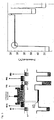
- FIG. 4A An actual sensor output characteristic was as shown in Fig. 4A.
- Fig. 4B shows a theoretical sensor output characteristic. If the flex point of an output curve is not clear as shown in Fig. 4A , accurate measurement is impossible. In other words, sufficient sensitivity is not obtained.
- the inventors intensively investigated to find the cause of drop of sensitivity, and found that the sensitivity is lowered because of accumulation of trace charges in the sensing part, regardlessly of chemical or physical phenomenon to be detected.
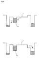
- a potential bump (barrier) 40 formed between the charge injection adjusting part 2 and the sensing part 3 as shown in Fig. 5 . Due to existence of this bump 40, at step 5, the charge not supposed to be accumulated is left over in the sensing part 3, and it is then transferred to the floating diffusion part 5 (see Fig. 6 ).
- a second cause lies in the charge trapped in the interface state of the sensing part 3.
- the residual charge is also transferred to the floating diffusion part and causes to lower the sensitivity (see Fig. 7 ).
- a first aspect of the invention has a configuration as described below.
- a charge accumulating type chemical and physical phenomenon detecting apparatus including a removing means for removing the charge remaining in the sensing part due to the potential bump formed between the sensing part and the charge injection adjusting part, from the sensing part.
- the charge remaining in the sensing part is removed by the removing means, it is not transferred to the floating diffusion part. Hence, the output characteristic is improved, and the sensitivity is enhanced.
- an elimination well is provided consecutively to the sensing part, and the charge remaining in this elimination well may be temporarily put aside.
- the elimination well can be provided in a simple structure of disposing electrodes, and thus the apparatus is not complicated. Therefore, an inexpensive apparatus can be presented
- the depth of a potential well of this elimination well is varied. More specifically, as shown in Fig. 9 , by lowering the potential of the elimination well 50 and increasing the depth of the well, the charge in the sensing part 3 is sucked into the elimination well 50. At this time, the bump 52 existing in the sensing part 3 disappears when a fringing field is formed by an electric field forming the elimination well 50. As a result, the charge existing in the sensing part 3 can be sucked in.
- the depth of the potential well of the elimination well is changed, but by forming a new elimination well, too, the residual charge in the sensing part can be sucked in.
- the charge sucked in the elimination well is desired to be removed from the elimination well.
- the potential of the charge injection adjusting part is set higher than that of the elimination well, and the charge in the elimination well is distributed into the charge supply unit.
- the charge may be trapped in the interface state existing between the silicon substrate corresponding to the sensing part 3 and the silicon oxide film, and it may take a long time until sucked completely in the elimination well or the floating diffusion part.
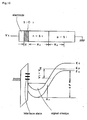
- the position of charge existing in the sensing part is preferred to be separated from the substrate surface. More specifically, by doping an n type impurity in the surface of a p type region for forming the sensing part, the charge existing position can be transferred from the substrate surface to its inside (see Fig. 10 ).
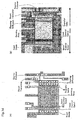
- FIG. 11 A charge accumulating type chemical and physical phenomenon detecting apparatus 60 of the embodiment is shown in Fig. 11 .
- same parts as in Fig. 1 are identified with same reference numerals and explanation is omitted.
- the apparatus 60 of the embodiment includes a gate electrode (first charge control electrode) 22 and an elimination electrode (second charge control electrode) 62 formed between a charge supply unit 1 and a sensing part 3.
- the elimination electrode 62 controls the potential of the elimination well 50.
- the surface of a p type region 15 is transformed to an n type by polysilicon. As a result, trapping of charge in the surface state of the sensing part 3 is prevented.
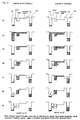
- Step 1 shows a standby state. In this standby state, as explained in Fig. 8 , the charge is remaining in the sensing part.
- step 3 the potential of the charge supply unit 1 is lowered, and the charge is supplied in the sensing part 3. And then, by raising the potential of the charge supply unit 1, the charge after being scooped by the charge supply unit 1 is left over in the sensing part 3 (step 5). At this time, if signal is not staying in the sensing part 3, as explained in Fig. 8 , a signal is also remaining.
- the charge remaining in the sensing part 3 is sucked into the elimination well 50. Since the substrate surface corresponding to the sensing part 3 is doped in the n type, the charge is not trapped on this surface. Therefore, the charge can be removed from the sensing part 3 in a short time.
- the potential of the elimination electrode 62 is raised, and the potential of the elimination well 50 is set deeper than the potential of the sensing part 3, but it may be set at the same potential as the sensing part 3, and at step 6, the potential of this part may set deeper.
- the potential of the barrier 4 is raised, and the charge in the sensing par 3 is transferred to the floating diffusion part 5.
- the sensing part 3 since charge due to the potential.bump is not left over, the remaining charge is not accumulated in the floating diffusion part 5.
- the substrate surface of the sensing part 3 is doped in the n type, charge is not trapped therein, and if a signal is staying, the whole amount of charge accumulated in the sensing part 3 can be transferred to the floating diffusion part 5 completely and in a short time.
- step 9 the potential of the elimination well 50 is returned to the standby state.
- the charge accumulated in the elimination well 50 should be discharged. Accordingly, for example, at step 8 shown in Fig. 13 , it is preferred to return the charge in the elimination well 50 to the charge supply unit 1 by raising the potential of the charge injection adjusting part 2.
- FIG. 14A A layout of the apparatus in the embodiment is shown in Fig. 14A . Its microscopic image is shown in Fig. 14B .
- the area of the sensing part 3 is 10000 ⁇ m 2
- the area of the floating diffusion part 5 is 1500 ⁇ m 2
- Film thickness of the silicon nitride film 23 as a cause of the potential bump is 0.1 ⁇ m.
- This apparatus was calibrated in pH standard solution 32.
- the output voltage when sweeping the reference voltage Vref is shown in Fig. 15 .
- a signal is issued even when the potential difference is zero (in a state not allowing a signal to stay) between the reference electrode 26 and the gate electrode 22.
- an ideal characteristic is shown in the apparatus 60 of the embodiment.
- the cumulative degree of charge from the sensing part 3 to the floating diffusion part is 1.
- a reference voltage Vref1 in central portion of its gradient is specified.
- the reference voltage is set at the specified Vref1, and different standard solutions are measured.
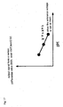
- the relation of pH and an output signal is known to be expressed in the following linear function.
- V is an output signal (voltage), in this case it is a differential value G (V) of a reset voltage and an output voltage.
- the differential value is expressed by the function G (V) of an output signal.
- This linear function is a calibration curve for defining the relation of a pH value and an output value.
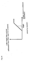
- Fig. 18 shows output changes by repetition of unit detection operations in the apparatus 60 of the embodiment.
- the axis of abscissas denotes the voltage value of reference electrode.
- pH 7 in this example
- output changes by repetition of unit detection operations are shown in Fig. 19 .
- Fig. 18 and Fig. 19 in the apparatus of the embodiment, it is known that noise is not superposed when charges are accumulated on the floating diffusion part by repeating the unit detection operations. As a result, the sensitivity is enhanced. In this embodiment, by repeating the unit detection operation by 10 times, the sensitivity is enhanced by about 10 times.
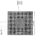
- Fig. 20 shows sensor chips including 10 vertical pieces and 10 lateral pieces of the apparatus shown in Fig. 11 .
- Each apparatus is immersed in a same aqueous solution, and a signal from each apparatus is displayed as a color or pattern image corresponding to the magnitude of the signal.
- Fig. 21 shows an example of an image display.
- the pixel for composing the image shown in Fig. 21 corresponds to each apparatus.
- Fig. 21 (a) shows the initial acidic solution, and pH changes of entire solution after adding an alkaline solution to this acidic solution are shown in Fig. 21 (b) and Fig. 21 (c) .
- Fig. 22 shows an array sensor consisting of 32 vertical pieces and 32 lateral pieces of the apparatus of the embodiment, and adding shift registers in the vertical and lateral directions.
- a chemical phenomenon detecting apparatus capable of detecting L-glutamic acid can be composed. Or by fixing DNA or antigen on the silicon nitride film, antigen or antibody of DNA can be detected. It is also possible to deposite a metal film and/or an SAM film (self-forming monomolecular film) on the silicon nitride film.
- a physical phenomenon detecting apparatus capable of measuring the temperature, pressure, or magnetism can be realized.
Landscapes
- Chemical & Material Sciences (AREA)
- Health & Medical Sciences (AREA)
- Life Sciences & Earth Sciences (AREA)
- Electrochemistry (AREA)
- Analytical Chemistry (AREA)
- Pathology (AREA)
- Immunology (AREA)
- Chemical Kinetics & Catalysis (AREA)
- Engineering & Computer Science (AREA)
- Physics & Mathematics (AREA)
- Microelectronics & Electronic Packaging (AREA)
- Biochemistry (AREA)
- General Health & Medical Sciences (AREA)
- General Physics & Mathematics (AREA)
- Molecular Biology (AREA)
- Computer Hardware Design (AREA)
- Investigating Or Analyzing Materials By The Use Of Electric Means (AREA)
Claims (7)
- Eine Detektionsvorrichtung vom Ladungsspeicherungstyp, aufweisend:• ein Messungs-Bestandteil (3), wobei das Potential hierbei von einem chemischen oder einem physikalischen Phänomen abhängig ist,• eine Ladungsversorgungseinheit (1) zum Bereitstellen einer Ladung an den Messungs-Bestandteil,• ein Ladungsinjektionsanpassungs-Bestandteil (2), der zwischen den Messungs-Bestandteil (3) und die Ladungsversorgungseinheit (1) gefügt ist, und• ein Fließend-Diffusions-Bestandteil (5) zum Speichern der Ladung, die von dem Messungs-Bestandteil transferiert wird, dadurch gekennzeichnet, dass• die Detektionsvorrichtung eine Eliminierungs-Elektrode (62) zum Bilden eines Eliminierungs-Walls (50) nachfolgend zu dem Messungs-Bestandteil (3) und zum Steuern des Potentials des Eliminierungs-Walls (50), um die Ladung, die in dem Messungs-Bestandteil gehalten wird, durch eine Potentialsenke, welche zwischen dem Messungs-Bestandteil (3) und dem Ladungsinjektionsanpassungs-Bestandteil (2) gebildet ist, abzusaugen, aufweist.
- Die Vorrichtung gemäß Anspruch 1, dadurch gekennzeichnet, dass die Eliminierungs-Elektrode (62) es erlaubt, eine Tiefe des Potentials des Eliminierungs-Walls (50) mittels eine angelegten Spannung zu variieren, sodass eine Ladungsmenge, die in den Eliminierungs-Walls (50) gesaugt wird, zu einer Ladungsmenge korrespondiert, die durch die Potentialsenke in dem Messungs-Bestandteil (3) gehalten wird.
- Die Vorrichtung gemäß einem der Ansprüche 1 oder 2, dadurch gekennzeichnet, dass die Eliminierungs-Elektrode (62) eine Steuerung erlaubt, sodass der Eliminierungs-Walls (50) eine Tiefe eines ersten Potential-Walls in einem Zustand, wenn eine Ladung von der Ladungsversorgungseinheit (1) an die Messungs-Bestandteil (3) geführt wird, zur Verfügung stellt, und eine Tiefe eines zweiten Potential-Walls in einem Zustand vor dem Transferieren der Ladung von dem Messungs-Bestandteil (3) an den Fließend-Diffusions-Bestandteil (5), zur Verfügung zu stellt, und die Tiefe des zweiten Potential-Walls tiefer ist als die Tiefe es ersten Potential-Walls.
- Die Vorrichtung gemäß einem der Ansprüche 1 bis 3, wobei der Eliminierungs-Wall (50) zwischen dem Ladungsinjektionsanpassungs-Bestandteil (2) und dem Messungs-Bestandteil (3) gebildet wird.
- Die Vorrichtung gemäß einem der Ansprüche 1 bis 4, weiterhin aufweisend ein Mittel zum Entladen der Ladung, die in dem Eliminierungs-Wall (50) gespeichert ist, in die Ladungsversorgungseinheit (1).
- The Vorrichtung gemäß einem der Ansprüche 1 bis 5, wobei die Ladung, die in dem Messungs-Bestandteil (3) existiert, von einer Oberfläche eines Substrates (10) entfernt angeordnet ist.
- Die Vorrichtung gemäß Anspruch 6, wobei das Substrat eine erste Region aufweist, die zumindest zu dem Messungs-Bestandteil (3) korrespondiert, und die mit einer Unreinheit eines ersten Leitungstyps dotiert ist, und eine zweite Region aufweist, die in der Oberfläche des Substrates (10) angeordnet ist, und die mit einer Unreinheit eines zweiten Leitungstyps dotiert ist, der verschieden ist von dem ersten Leitungstyp, und die Ladung innerhalb des Substrats angeordnet ist.
Applications Claiming Priority (2)
| Application Number | Priority Date | Filing Date | Title |
|---|---|---|---|
| JP2005069501 | 2005-03-11 | ||
| PCT/JP2006/304868 WO2006095903A1 (ja) | 2005-03-11 | 2006-03-13 | 累積型化学・物理現象検出装置 |
Publications (3)
| Publication Number | Publication Date |
|---|---|
| EP1870703A1 EP1870703A1 (de) | 2007-12-26 |
| EP1870703A4 EP1870703A4 (de) | 2011-09-14 |
| EP1870703B1 true EP1870703B1 (de) | 2014-04-02 |
Family
ID=36953487
Family Applications (1)
| Application Number | Title | Priority Date | Filing Date |
|---|---|---|---|
| EP06715591.1A Expired - Lifetime EP1870703B1 (de) | 2005-03-11 | 2006-03-13 | Kumulative Nachweisvorrichtung für chemische oder physikalische Phänomene |
Country Status (5)
| Country | Link |
|---|---|
| US (1) | US7826980B2 (de) |
| EP (1) | EP1870703B1 (de) |
| JP (1) | JP4171820B2 (de) |
| KR (2) | KR101269508B1 (de) |
| WO (1) | WO2006095903A1 (de) |
Cited By (18)
| Publication number | Priority date | Publication date | Assignee | Title |
|---|---|---|---|---|
| US8692298B2 (en) | 2006-12-14 | 2014-04-08 | Life Technologies Corporation | Chemical sensor array having multiple sensors per well |
| US8698212B2 (en) | 2009-05-29 | 2014-04-15 | Life Technologies Corporation | Active chemically-sensitive sensors |
| US8731847B2 (en) | 2010-06-30 | 2014-05-20 | Life Technologies Corporation | Array configuration and readout scheme |
| US8742472B2 (en) | 2006-12-14 | 2014-06-03 | Life Technologies Corporation | Chemically sensitive sensors with sample and hold capacitors |
| US8776573B2 (en) | 2009-05-29 | 2014-07-15 | Life Technologies Corporation | Methods and apparatus for measuring analytes |
| US8786331B2 (en) | 2012-05-29 | 2014-07-22 | Life Technologies Corporation | System for reducing noise in a chemical sensor array |
| US8796036B2 (en) | 2010-09-24 | 2014-08-05 | Life Technologies Corporation | Method and system for delta double sampling |
| US8821798B2 (en) | 2012-01-19 | 2014-09-02 | Life Technologies Corporation | Titanium nitride as sensing layer for microwell structure |
| US8841217B1 (en) | 2013-03-13 | 2014-09-23 | Life Technologies Corporation | Chemical sensor with protruded sensor surface |
| US8858782B2 (en) | 2010-06-30 | 2014-10-14 | Life Technologies Corporation | Ion-sensing charge-accumulation circuits and methods |
| US8936763B2 (en) | 2008-10-22 | 2015-01-20 | Life Technologies Corporation | Integrated sensor arrays for biological and chemical analysis |
| US8962366B2 (en) | 2013-01-28 | 2015-02-24 | Life Technologies Corporation | Self-aligned well structures for low-noise chemical sensors |
| US8963216B2 (en) | 2013-03-13 | 2015-02-24 | Life Technologies Corporation | Chemical sensor with sidewall spacer sensor surface |
| US9080968B2 (en) | 2013-01-04 | 2015-07-14 | Life Technologies Corporation | Methods and systems for point of use removal of sacrificial material |
| US9116117B2 (en) | 2013-03-15 | 2015-08-25 | Life Technologies Corporation | Chemical sensor with sidewall sensor surface |
| US9128044B2 (en) | 2013-03-15 | 2015-09-08 | Life Technologies Corporation | Chemical sensors with consistent sensor surface areas |
| US9194000B2 (en) | 2008-06-25 | 2015-11-24 | Life Technologies Corporation | Methods and apparatus for measuring analytes using large scale FET arrays |
| US9404920B2 (en) | 2006-12-14 | 2016-08-02 | Life Technologies Corporation | Methods and apparatus for detecting molecular interactions using FET arrays |
Families Citing this family (27)
| Publication number | Priority date | Publication date | Assignee | Title |
|---|---|---|---|---|
| JP5335415B2 (ja) * | 2006-03-20 | 2013-11-06 | 国立大学法人豊橋技術科学大学 | 累積型化学・物理現象検出方法及びその装置 |
| US11339430B2 (en) | 2007-07-10 | 2022-05-24 | Life Technologies Corporation | Methods and apparatus for measuring analytes using large scale FET arrays |
| EP2224230B1 (de) * | 2007-12-20 | 2019-03-20 | National University Corporation Toyohashi University of Technology | Kombidetektor |
| JP5077799B2 (ja) * | 2008-03-25 | 2012-11-21 | 国立大学法人豊橋技術科学大学 | 化学・物理現象検出装置及びその制御方法 |
| US20120261274A1 (en) | 2009-05-29 | 2012-10-18 | Life Technologies Corporation | Methods and apparatus for measuring analytes |
| EP2588850B1 (de) | 2010-06-30 | 2016-12-28 | Life Technologies Corporation | Trockentestverfahren für isfet-arrays |
| US11307166B2 (en) | 2010-07-01 | 2022-04-19 | Life Technologies Corporation | Column ADC |
| US8653567B2 (en) | 2010-07-03 | 2014-02-18 | Life Technologies Corporation | Chemically sensitive sensor with lightly doped drains |
| WO2012036679A1 (en) | 2010-09-15 | 2012-03-22 | Life Technologies Corporation | Methods and apparatus for measuring analytes |
| JP5773357B2 (ja) * | 2011-07-01 | 2015-09-02 | 国立大学法人豊橋技術科学大学 | 化学・物理現象検出装置及び検出方法 |
| KR101909915B1 (ko) | 2011-07-14 | 2018-10-19 | 고꾸리쯔 다이가꾸 호우징 도요하시 기쥬쯔 가가꾸 다이가꾸 | 화학·물리현상 검출방법 및 그 장치 |
| US9482641B2 (en) | 2011-08-12 | 2016-11-01 | National University Corporation Toyohashi University Of Technology | Device and method for detecting chemical and physical phenomena |
| US9970984B2 (en) | 2011-12-01 | 2018-05-15 | Life Technologies Corporation | Method and apparatus for identifying defects in a chemical sensor array |
| US9599586B2 (en) * | 2012-08-27 | 2017-03-21 | Infineon Technologies Ag | Ion sensor |
| US9841398B2 (en) | 2013-01-08 | 2017-12-12 | Life Technologies Corporation | Methods for manufacturing well structures for low-noise chemical sensors |
| CN105264366B (zh) | 2013-03-15 | 2019-04-16 | 生命科技公司 | 具有一致传感器表面区域的化学传感器 |
| WO2014149779A1 (en) | 2013-03-15 | 2014-09-25 | Life Technologies Corporation | Chemical device with thin conductive element |
| US9835585B2 (en) | 2013-03-15 | 2017-12-05 | Life Technologies Corporation | Chemical sensor with protruded sensor surface |
| US20140336063A1 (en) | 2013-05-09 | 2014-11-13 | Life Technologies Corporation | Windowed Sequencing |
| US10458942B2 (en) | 2013-06-10 | 2019-10-29 | Life Technologies Corporation | Chemical sensor array having multiple sensors per well |
| JP6228098B2 (ja) * | 2014-10-20 | 2017-11-08 | シャープ株式会社 | 化学・物理現象検出装置及びその製造方法 |
| KR102593647B1 (ko) | 2014-12-18 | 2023-10-26 | 라이프 테크놀로지스 코포레이션 | 트랜스미터 구성을 갖춘 높은 데이터율 집적 회로 |
| US10077472B2 (en) | 2014-12-18 | 2018-09-18 | Life Technologies Corporation | High data rate integrated circuit with power management |
| WO2016100521A1 (en) | 2014-12-18 | 2016-06-23 | Life Technologies Corporation | Methods and apparatus for measuring analytes using large scale fet arrays |
| EP3246699B1 (de) * | 2015-01-14 | 2019-04-17 | National University Corporation TOYOHASHI UNIVERSITY OF TECHNOLOGY | Vorrichtung zum nachweis chemischer/physikalischer phänomene |
| EP3273233B8 (de) * | 2015-03-19 | 2022-08-03 | National University Corporation Toyohashi University Of Technology | Verfahren zur steuerung einer vorrichtung zur erkennung chemischer/physikalischer phänomene |
| JP7270920B2 (ja) * | 2018-10-22 | 2023-05-11 | 国立大学法人豊橋技術科学大学 | 化学・物理現象検出素子 |
Family Cites Families (20)
| Publication number | Priority date | Publication date | Assignee | Title |
|---|---|---|---|---|
| JPS5567165A (en) * | 1978-11-15 | 1980-05-21 | Matsushita Electronics Corp | Semiconductor device |
| FR2504334B1 (fr) * | 1981-04-16 | 1985-10-18 | Thomson Csf | Dispositif d'analyse d'image en lignes successives, utilisant le transfert de charges electriques, composant une memoire de ligne, et camera de television comportant un tel dispositif |
| JPS59225344A (ja) * | 1983-06-06 | 1984-12-18 | Sanken Electric Co Ltd | イオンセンサ−用絶縁ゲ−ト電界効果トランジスタ |
| JPS6138624A (ja) | 1984-07-31 | 1986-02-24 | Ebara Corp | 灰固化設備の製品分配装置 |
| JPS61131854U (de) * | 1985-02-06 | 1986-08-18 | ||
| JPS62132160A (ja) * | 1985-12-04 | 1987-06-15 | Terumo Corp | 分離ゲ−ト型isfetを用いたバイオセンサ− |
| US5247554A (en) * | 1987-01-16 | 1993-09-21 | Kabushiki Kaisha Toshiba | Charge detection circuit |
| JPH04100384A (ja) | 1990-08-17 | 1992-04-02 | Mitsubishi Electric Corp | T・d・i動作固体撮像装置 |
| JPH05335549A (ja) * | 1992-06-01 | 1993-12-17 | Matsushita Electric Ind Co Ltd | 固体撮像装置およびその駆動方法 |
| JP3129528B2 (ja) | 1992-07-01 | 2001-01-31 | 明治乳業株式会社 | 風味及び保存安定性の良好な液状発酵乳の製造法 |
| JP4231560B2 (ja) * | 1997-05-29 | 2009-03-04 | 株式会社堀場製作所 | 化学量の分布の電気化学的測定方法および装置 |
| JP4183789B2 (ja) * | 1998-01-14 | 2008-11-19 | 株式会社堀場製作所 | 物理現象および/または化学現象の検出装置 |
| JP4257874B2 (ja) | 1998-04-23 | 2009-04-22 | 信越ポリマー株式会社 | トップカバーテープ |
| JP3659122B2 (ja) * | 2000-03-22 | 2005-06-15 | 日本電気株式会社 | 電荷転送装置 |
| JP3623728B2 (ja) | 2000-09-27 | 2005-02-23 | 独立行政法人科学技術振興機構 | 累積型化学・物理現象検出装置 |
| US7049645B2 (en) * | 2001-11-16 | 2006-05-23 | Bio-X Inc. | FET type sensor, ion density detecting method comprising this sensor, and base sequence detecting method |
| JP4137442B2 (ja) * | 2001-12-28 | 2008-08-20 | 富士フイルム株式会社 | 固体撮像装置とそのスミア電荷除去方法並びにデジタルスチルカメラ |
| JP2004071696A (ja) * | 2002-08-02 | 2004-03-04 | Semiconductor Energy Lab Co Ltd | 半導体装置及びその作製方法 |
| JP4678676B2 (ja) * | 2004-12-10 | 2011-04-27 | 株式会社堀場製作所 | 物理現象または化学現象の測定方法または測定装置 |
| JP4768538B2 (ja) * | 2006-07-21 | 2011-09-07 | 京セラミタ株式会社 | 画像読取装置及び該方法 |
-
2006
- 2006-03-13 EP EP06715591.1A patent/EP1870703B1/de not_active Expired - Lifetime
- 2006-03-13 KR KR1020077020633A patent/KR101269508B1/ko not_active Expired - Lifetime
- 2006-03-13 WO PCT/JP2006/304868 patent/WO2006095903A1/ja not_active Ceased
- 2006-03-13 US US11/886,130 patent/US7826980B2/en active Active
- 2006-03-13 KR KR1020137004786A patent/KR101343044B1/ko not_active Expired - Lifetime
- 2006-03-13 JP JP2007507224A patent/JP4171820B2/ja not_active Expired - Lifetime
Cited By (36)
| Publication number | Priority date | Publication date | Assignee | Title |
|---|---|---|---|---|
| US9023189B2 (en) | 2006-12-14 | 2015-05-05 | Life Technologies Corporation | High density sensor array without wells |
| US9134269B2 (en) | 2006-12-14 | 2015-09-15 | Life Technologies Corporation | Methods and apparatus for measuring analytes using large scale FET arrays |
| US9404920B2 (en) | 2006-12-14 | 2016-08-02 | Life Technologies Corporation | Methods and apparatus for detecting molecular interactions using FET arrays |
| US9269708B2 (en) | 2006-12-14 | 2016-02-23 | Life Technologies Corporation | Methods and apparatus for measuring analytes using large scale FET arrays |
| US8742472B2 (en) | 2006-12-14 | 2014-06-03 | Life Technologies Corporation | Chemically sensitive sensors with sample and hold capacitors |
| US8764969B2 (en) | 2006-12-14 | 2014-07-01 | Life Technologies Corporation | Methods for operating chemically sensitive sensors with sample and hold capacitors |
| US8890216B2 (en) | 2006-12-14 | 2014-11-18 | Life Technologies Corporation | Methods and apparatus for measuring analytes using large scale FET arrays |
| US8692298B2 (en) | 2006-12-14 | 2014-04-08 | Life Technologies Corporation | Chemical sensor array having multiple sensors per well |
| US9194000B2 (en) | 2008-06-25 | 2015-11-24 | Life Technologies Corporation | Methods and apparatus for measuring analytes using large scale FET arrays |
| US8936763B2 (en) | 2008-10-22 | 2015-01-20 | Life Technologies Corporation | Integrated sensor arrays for biological and chemical analysis |
| US8742469B2 (en) | 2009-05-29 | 2014-06-03 | Life Technologies Corporation | Active chemically-sensitive sensors with correlated double sampling |
| US8766327B2 (en) | 2009-05-29 | 2014-07-01 | Life Technologies Corporation | Active chemically-sensitive sensors with in-sensor current sources |
| US8698212B2 (en) | 2009-05-29 | 2014-04-15 | Life Technologies Corporation | Active chemically-sensitive sensors |
| US8994076B2 (en) | 2009-05-29 | 2015-03-31 | Life Technologies Corporation | Chemically-sensitive field effect transistor based pixel array with protection diodes |
| US8822205B2 (en) | 2009-05-29 | 2014-09-02 | Life Technologies Corporation | Active chemically-sensitive sensors with source follower amplifier |
| US8776573B2 (en) | 2009-05-29 | 2014-07-15 | Life Technologies Corporation | Methods and apparatus for measuring analytes |
| US8912580B2 (en) | 2009-05-29 | 2014-12-16 | Life Technologies Corporation | Active chemically-sensitive sensors with in-sensor current sources |
| US8772698B2 (en) | 2010-06-30 | 2014-07-08 | Life Technologies Corporation | CCD-based multi-transistor active pixel sensor array |
| US8731847B2 (en) | 2010-06-30 | 2014-05-20 | Life Technologies Corporation | Array configuration and readout scheme |
| US8742471B2 (en) | 2010-06-30 | 2014-06-03 | Life Technologies Corporation | Chemical sensor array with leakage compensation circuit |
| US8823380B2 (en) | 2010-06-30 | 2014-09-02 | Life Technologies Corporation | Capacitive charge pump |
| US8858782B2 (en) | 2010-06-30 | 2014-10-14 | Life Technologies Corporation | Ion-sensing charge-accumulation circuits and methods |
| US9239313B2 (en) | 2010-06-30 | 2016-01-19 | Life Technologies Corporation | Ion-sensing charge-accumulation circuits and methods |
| US8741680B2 (en) | 2010-06-30 | 2014-06-03 | Life Technologies Corporation | Two-transistor pixel array |
| US8912005B1 (en) | 2010-09-24 | 2014-12-16 | Life Technologies Corporation | Method and system for delta double sampling |
| US8796036B2 (en) | 2010-09-24 | 2014-08-05 | Life Technologies Corporation | Method and system for delta double sampling |
| US9110015B2 (en) | 2010-09-24 | 2015-08-18 | Life Technologies Corporation | Method and system for delta double sampling |
| US8821798B2 (en) | 2012-01-19 | 2014-09-02 | Life Technologies Corporation | Titanium nitride as sensing layer for microwell structure |
| US8786331B2 (en) | 2012-05-29 | 2014-07-22 | Life Technologies Corporation | System for reducing noise in a chemical sensor array |
| US9270264B2 (en) | 2012-05-29 | 2016-02-23 | Life Technologies Corporation | System for reducing noise in a chemical sensor array |
| US9080968B2 (en) | 2013-01-04 | 2015-07-14 | Life Technologies Corporation | Methods and systems for point of use removal of sacrificial material |
| US8962366B2 (en) | 2013-01-28 | 2015-02-24 | Life Technologies Corporation | Self-aligned well structures for low-noise chemical sensors |
| US8963216B2 (en) | 2013-03-13 | 2015-02-24 | Life Technologies Corporation | Chemical sensor with sidewall spacer sensor surface |
| US8841217B1 (en) | 2013-03-13 | 2014-09-23 | Life Technologies Corporation | Chemical sensor with protruded sensor surface |
| US9128044B2 (en) | 2013-03-15 | 2015-09-08 | Life Technologies Corporation | Chemical sensors with consistent sensor surface areas |
| US9116117B2 (en) | 2013-03-15 | 2015-08-25 | Life Technologies Corporation | Chemical sensor with sidewall sensor surface |
Also Published As
| Publication number | Publication date |
|---|---|
| WO2006095903A1 (ja) | 2006-09-14 |
| US7826980B2 (en) | 2010-11-02 |
| US20080231253A1 (en) | 2008-09-25 |
| KR20130028980A (ko) | 2013-03-20 |
| JP4171820B2 (ja) | 2008-10-29 |
| JPWO2006095903A1 (ja) | 2008-08-21 |
| EP1870703A1 (de) | 2007-12-26 |
| KR101269508B1 (ko) | 2013-05-30 |
| EP1870703A4 (de) | 2011-09-14 |
| KR20070119012A (ko) | 2007-12-18 |
| KR101343044B1 (ko) | 2013-12-18 |
Similar Documents
| Publication | Publication Date | Title |
|---|---|---|
| EP1870703B1 (de) | Kumulative Nachweisvorrichtung für chemische oder physikalische Phänomene | |
| JP4231560B2 (ja) | 化学量の分布の電気化学的測定方法および装置 | |
| KR101087565B1 (ko) | 광검출기 및 이를 이용한 공간 정보 검출 장치 | |
| US6294133B1 (en) | Multiple detecting apparatus for physical phenomenon and/or chemical phenomenon | |
| JPH10332423A5 (de) | ||
| JP5637244B2 (ja) | 累積型化学・物理現象検出装置及びその制御方法 | |
| JP2006284225A (ja) | ポテンシャルの測定方法および測定装置 | |
| WO2010001277A1 (en) | Chip integrated ion sensor | |
| CN105684150B (zh) | 线性图像传感器 | |
| EP3273233B1 (de) | Verfahren zur steuerung einer vorrichtung zur erkennung chemischer/physikalischer phänomene | |
| EP3246699B1 (de) | Vorrichtung zum nachweis chemischer/physikalischer phänomene | |
| JP4641444B2 (ja) | 物理現象または化学現象に係るポテンシャル測定装置 | |
| EP2264767B1 (de) | Festkörper-bilderfassungsgerät mit elektronenmultiplikationsfunktion | |
| EP1278060A1 (de) | CCD Sensor | |
| US6667499B1 (en) | Solid-state image sensing device and method of manufacturing the same | |
| KR20140042825A (ko) | 화학·물리현상 검출방법 및 그 장치 | |
| US20050212938A1 (en) | CCD linear sensor | |
| CN116635714B (zh) | 离子传感器及离子传感器的制造方法 | |
| JP6522150B2 (ja) | イオン濃度センサ | |
| US12196703B2 (en) | Ion detection device and ion detection method | |
| KR20020044204A (ko) | 이미지센서 단위 픽셀의 베리어 포텐셜 측정 방법 | |
| JPH0774335A (ja) | 固体撮像素子 | |
| JPH0786548A (ja) | イメ−ジセンサ |
Legal Events
| Date | Code | Title | Description |
|---|---|---|---|
| PUAI | Public reference made under article 153(3) epc to a published international application that has entered the european phase |
Free format text: ORIGINAL CODE: 0009012 |
|
| 17P | Request for examination filed |
Effective date: 20071009 |
|
| AK | Designated contracting states |
Kind code of ref document: A1 Designated state(s): DE FR |
|
| RIN1 | Information on inventor provided before grant (corrected) |
Inventor name: MARUYAMA, YUKI Inventor name: SAWADA, KAZUAKI Inventor name: HIZAWA, TAKESHI Inventor name: MATSUO, JUNICHI, |
|
| DAX | Request for extension of the european patent (deleted) | ||
| RBV | Designated contracting states (corrected) |
Designated state(s): DE FR |
|
| A4 | Supplementary search report drawn up and despatched |
Effective date: 20110818 |
|
| RIC1 | Information provided on ipc code assigned before grant |
Ipc: G01N 27/416 20060101ALI20110811BHEP Ipc: G01N 27/414 20060101AFI20110811BHEP Ipc: G01N 27/00 20060101ALI20110811BHEP |
|
| 17Q | First examination report despatched |
Effective date: 20120612 |
|
| GRAP | Despatch of communication of intention to grant a patent |
Free format text: ORIGINAL CODE: EPIDOSNIGR1 |
|
| INTG | Intention to grant announced |
Effective date: 20131018 |
|
| RIN1 | Information on inventor provided before grant (corrected) |
Inventor name: MARUYAMA, YUKI Inventor name: HIZAWA, TAKESHI Inventor name: MATSUO, JUNICHI, Inventor name: SAWADA, KAZUAKI |
|
| GRAS | Grant fee paid |
Free format text: ORIGINAL CODE: EPIDOSNIGR3 |
|
| GRAA | (expected) grant |
Free format text: ORIGINAL CODE: 0009210 |
|
| AK | Designated contracting states |
Kind code of ref document: B1 Designated state(s): DE FR |
|
| REG | Reference to a national code |
Ref country code: DE Ref legal event code: R096 Ref document number: 602006040905 Country of ref document: DE Effective date: 20140515 |
|
| RAP2 | Party data changed (patent owner data changed or rights of a patent transferred) |
Owner name: NATIONAL UNIVERSITY CORPORATION TOYOHASHI UNIVERSI |
|
| REG | Reference to a national code |
Ref country code: DE Ref legal event code: R097 Ref document number: 602006040905 Country of ref document: DE |
|
| PLBE | No opposition filed within time limit |
Free format text: ORIGINAL CODE: 0009261 |
|
| STAA | Information on the status of an ep patent application or granted ep patent |
Free format text: STATUS: NO OPPOSITION FILED WITHIN TIME LIMIT |
|
| 26N | No opposition filed |
Effective date: 20150106 |
|
| REG | Reference to a national code |
Ref country code: FR Ref legal event code: PLFP Year of fee payment: 10 |
|
| REG | Reference to a national code |
Ref country code: DE Ref legal event code: R097 Ref document number: 602006040905 Country of ref document: DE Effective date: 20150106 |
|
| REG | Reference to a national code |
Ref country code: DE Ref legal event code: R082 Ref document number: 602006040905 Country of ref document: DE Representative=s name: KUHNEN & WACKER PATENT- UND RECHTSANWALTSBUERO, DE |
|
| REG | Reference to a national code |
Ref country code: FR Ref legal event code: PLFP Year of fee payment: 11 |
|
| REG | Reference to a national code |
Ref country code: FR Ref legal event code: PLFP Year of fee payment: 12 |
|
| REG | Reference to a national code |
Ref country code: FR Ref legal event code: PLFP Year of fee payment: 13 |
|
| REG | Reference to a national code |
Ref country code: DE Ref legal event code: R082 Ref document number: 602006040905 Country of ref document: DE Representative=s name: WITTHOFF JAEKEL STEINECKE PATENTANWAELTE PARTG, DE |
|
| PGFP | Annual fee paid to national office [announced via postgrant information from national office to epo] |
Ref country code: DE Payment date: 20250319 Year of fee payment: 20 |
|
| PGFP | Annual fee paid to national office [announced via postgrant information from national office to epo] |
Ref country code: FR Payment date: 20250325 Year of fee payment: 20 |
|
| REG | Reference to a national code |
Ref country code: DE Ref legal event code: R071 Ref document number: 602006040905 Country of ref document: DE |