EP1870965A1 - Procédé et appareil pour broche de connecteur à remplacement à chaud intégrée pour systèmes d'alimentation électrique CA ou CC - Google Patents
Procédé et appareil pour broche de connecteur à remplacement à chaud intégrée pour systèmes d'alimentation électrique CA ou CC Download PDFInfo
- Publication number
- EP1870965A1 EP1870965A1 EP07110849A EP07110849A EP1870965A1 EP 1870965 A1 EP1870965 A1 EP 1870965A1 EP 07110849 A EP07110849 A EP 07110849A EP 07110849 A EP07110849 A EP 07110849A EP 1870965 A1 EP1870965 A1 EP 1870965A1
- Authority
- EP
- European Patent Office
- Prior art keywords
- pin
- female
- female pin
- hot swap
- male
- Prior art date
- Legal status (The legal status is an assumption and is not a legal conclusion. Google has not performed a legal analysis and makes no representation as to the accuracy of the status listed.)
- Withdrawn
Links
- 238000000034 method Methods 0.000 title claims abstract description 40
- 239000004020 conductor Substances 0.000 claims abstract description 9
- 238000003780 insertion Methods 0.000 claims description 54
- 230000037431 insertion Effects 0.000 claims description 54
- 238000000605 extraction Methods 0.000 claims description 29
- 239000007787 solid Substances 0.000 claims description 13
- 230000007423 decrease Effects 0.000 claims description 8
- 230000003247 decreasing effect Effects 0.000 claims description 8
- 230000001965 increasing effect Effects 0.000 claims description 8
- 239000000463 material Substances 0.000 claims description 5
- 239000011796 hollow space material Substances 0.000 claims description 4
- 238000010586 diagram Methods 0.000 description 14
- 230000008569 process Effects 0.000 description 12
- 239000003990 capacitor Substances 0.000 description 10
- 230000006870 function Effects 0.000 description 10
- 238000001514 detection method Methods 0.000 description 9
- 230000013011 mating Effects 0.000 description 7
- 230000001052 transient effect Effects 0.000 description 7
- 230000000694 effects Effects 0.000 description 5
- 230000001939 inductive effect Effects 0.000 description 5
- 230000008859 change Effects 0.000 description 4
- 238000002955 isolation Methods 0.000 description 4
- 238000004891 communication Methods 0.000 description 3
- 238000012163 sequencing technique Methods 0.000 description 3
- 230000004913 activation Effects 0.000 description 2
- 230000002411 adverse Effects 0.000 description 2
- 238000006243 chemical reaction Methods 0.000 description 2
- 230000000593 degrading effect Effects 0.000 description 2
- 230000001419 dependent effect Effects 0.000 description 2
- 238000012886 linear function Methods 0.000 description 2
- 238000012423 maintenance Methods 0.000 description 2
- 230000001105 regulatory effect Effects 0.000 description 2
- 230000002441 reversible effect Effects 0.000 description 2
- 230000035939 shock Effects 0.000 description 2
- 230000002159 abnormal effect Effects 0.000 description 1
- 238000004378 air conditioning Methods 0.000 description 1
- 238000013461 design Methods 0.000 description 1
- 230000036541 health Effects 0.000 description 1
- 239000011810 insulating material Substances 0.000 description 1
- 230000010354 integration Effects 0.000 description 1
- 238000004519 manufacturing process Methods 0.000 description 1
- 230000000116 mitigating effect Effects 0.000 description 1
- 238000012544 monitoring process Methods 0.000 description 1
- 230000008439 repair process Effects 0.000 description 1
- 230000011664 signaling Effects 0.000 description 1
Images


Classifications
-
- H—ELECTRICITY
- H01—ELECTRIC ELEMENTS
- H01R—ELECTRICALLY-CONDUCTIVE CONNECTIONS; STRUCTURAL ASSOCIATIONS OF A PLURALITY OF MUTUALLY-INSULATED ELECTRICAL CONNECTING ELEMENTS; COUPLING DEVICES; CURRENT COLLECTORS
- H01R13/00—Details of coupling devices of the kinds covered by groups H01R12/70 or H01R24/00 - H01R33/00
- H01R13/02—Contact members
- H01R13/03—Contact members characterised by the material, e.g. plating, or coating materials
-
- H—ELECTRICITY
- H01—ELECTRIC ELEMENTS
- H01R—ELECTRICALLY-CONDUCTIVE CONNECTIONS; STRUCTURAL ASSOCIATIONS OF A PLURALITY OF MUTUALLY-INSULATED ELECTRICAL CONNECTING ELEMENTS; COUPLING DEVICES; CURRENT COLLECTORS
- H01R13/00—Details of coupling devices of the kinds covered by groups H01R12/70 or H01R24/00 - H01R33/00
- H01R13/66—Structural association with built-in electrical component
- H01R13/6608—Structural association with built-in electrical component with built-in single component
- H01R13/6616—Structural association with built-in electrical component with built-in single component with resistor
Definitions
- the present invention relates to connector pin systems, and more particularly to a method and apparatus for hot swap of modules using connector pin systems.
- Electric systems used in complex environments such as aerospace systems, more electric aircraft systems, industrial environments, vehicles, etc., include a large number of electric modules.
- Various electric modules may need to be extracted and replaced with other electric modules, to change functionality or to replace electric modules that exhibit faults.
- Hot swap, hot-plug, and hot-dock are terms used interchangeably to refer to the process of safely inserting or removing cards, PC boards, cables, and/or modules from a host system without removing power.
- the goal of hot swap is to insert or remove modules without disturbing, damaging, or degrading up/down-stream adjacent line replaceable modules/ subsystems, to increase system availability, reduce down time, simplify system repair, and allow for system maintenance/upgrade without interrupting service to other loads.
- hot swap can cause severe electrical, mechanical, thermal and operational problems in an electrical system.
- random pin arcing may occur during the mating process of a replaceable module with its parent electrical system.
- Pulling a board/module out while there is current passing through the module connectors, or inserting a board/module with all bulk/bypass capacitors at zero volts, can introduce severe electrical voltage/ current transients which may adversely impact reliability and lead to safety consequences.
- current chopping introduces Ldi / dt variations (where L is inductance of a load, for example) leading to very large voltage transients which are a major safety concern for maintenance people, as large voltage transients can cause high voltage electrical shock.
- a hot swap system for hot swap of modules includes a connector with long and short pins, a fuse, and an RC circuit.
- the long pins mate first, adding the RC circuit to pre-charge the module/board.
- the short pins mate, bypassing the resistor connected to the longer pins and creating a low impedance connection.
- One problem associated with long/short pin arrangements is the increase in number of pins needed for hot swap. Presence of more pins for hot swap leads to increased cost and weight of systems using such hot swap pin arrangements.
- a second problem associated with long/short pin arrangements for hot swap is lack of control in the timing of pin insertion and extraction during hot swap.
- a male connector pin is made of a conductive material, an outer layer of resistive material, and a layer of insulating material.
- the outer layer of resistive material is deposited on a first portion of the conductive material.
- the insulating layer separates the resistive layer from the conductive material.
- a disclosed embodiment of the application addresses these and other issues by utilizing an integrated hot swap connector pin system that includes a conductive male pin, and a female pin with a resistive region, an insulating region, and a conductive region.
- the method and apparatus produce a gradually decreasing resistance as the male pin is inserted into the female pin, hence eliminating in-rush currents during hot swap insertion of a replaceable module into a live power board.
- the method and apparatus produce a gradually increasing resistance as the male pin is extracted from the female pin, hence reducing current chopping during hot swap extraction of a replaceable module from a live power board.
- the method and apparatus prevent random pin arcing during mating process by reducing the AC or DC current during the MAKE or BREAK process; eliminate in-rush currents during initial insertion of a board/module with all bulk/bypass capacitors at zero volts; eliminate large electrical voltage/ current transients, such as large voltage transients due to Ldi / dt current chopping variations, which may adversely impact reliability and lead to safety consequences; provide a uniform and well controlled hot swap of replaceable modules and boards.
- a pin system for AC and DC electric power systems comprises: a female pin, the female pin comprising a resistive region, the resistive region forming a first portion of an inner surface of the female pin, and a conductive region, the conductive region forming a second portion of the inner surface of the female pin, the conductive region contacting the resistive region, the conductive region being located further than the resistive region from an open end of the female pin; and a male pin adapted to be inserted in the female pin along the inner surface of the female pin, the male pin being made of a conductive material.
- an apparatus for hot swap of AC or DC line replaceable modules comprises: a pin system, the pin system being connectable to a replaceable module and connectable to a backplane, the pin system comprising a female pin connectable to the backplane, the female pin comprising a resistive region forming a first portion of an inner surface of the female pin, and a conductive region forming a second portion of the inner surface of the female pin, the conductive region contacting the resistive region, the conductive region being located further than the resistive region from an open end of the female pin, and a male pin adapted to be inserted in the female pin along the inner surface of the female pin, the male pin being made of a conductive material, and the male pin being connectable to the replaceable module, wherein resistance of the pin system decreases in a continuous manner as the male pin is inserted into the female pin along the resistive region and the conductive region of the female pin; and a hot swap detector connectable to the pin system, the hot swap detector
- a method for hot swap of AC or DC line replaceable modules comprises: providing a female pin for connection to a backplane, the female pin comprising a resistive region comprising a first hollow cylindrical shell forming a first portion of an inner surface of the female pin, and a conductive region comprising a second hollow cylindrical shell forming a second portion of the inner surface of the female pin, a start of a base of the conductive region contacting an end of a base of the resistive region, the conductive region being located further than the resistive region from an open end of the female pin; providing a male pin for connection to a line replaceable module, the male pin being adapted for insertion in the female pin along an inner hollow space of the female pin, the male pin being made of a conductive solid cylindrical material to fill the inner hollow space of the female pin; decreasing a resistance between the line replaceable module and the backplane in a continuous manner as the male pin is inserted into the female pin along the resistive region and the conductive region of the
- a method for hot swap of AC or DC line replaceable modules comprises: providing a female pin for connection to a backplane; providing a male pin for connection to a line replaceable module, the male pin being adapted for insertion in the female pin; decreasing a resistance between the line replaceable module and the backplane in a continuous manner as the male pin is inserted into the female pin along a resistive region of the female pin and a conductive region of the female pin; and increasing a resistance between the line replaceable module and the backplane in a continuous manner as the male pin is extracted from the female pin along the conductive region and the resistive region of the female pin.
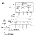
- FIG. 1 is a general functional block diagram of a subassembly electrical system containing line replaceable modules (LRMs) with hot-swap capability according to an embodiment of the present invention
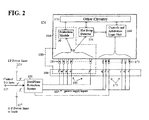
- FIG. 2 is a block diagram of an electrical configuration containing an integrated hot swap connector pins arrangement for hot swap of line replaceable modules according to an embodiment of the present invention
- FIG. 3 illustrates an integrated hot swap connector pins arrangement for hot swap of line replaceable modules according to an embodiment of the present invention
- FIG. 4 is a block diagram illustrating an exemplary implementation of a hot swap protection system using an integrated hot swap connector pins arrangement according to an embodiment of the present invention illustrated in FIG. 3;
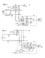
- FIG. 5 is a block diagram of an electrical configuration illustrating aspects of the operation of an integrated hot swap connector pins arrangement for detection of hot swap of line replaceable modules for DC input power according to an embodiment of the present invention illustrated in FIG. 3;
- FIG. 6 is a block diagram of an electrical configuration illustrating aspects of the operation of an integrated hot swap connector pins arrangement for detection of hot swap of line replaceable modules for AC input power according to an embodiment of the present invention illustrated in FIG. 3.
- FIG. 1 is a general functional block diagram of a subassembly electrical system containing line replaceable modules (LRMs) with hot-swap capability according to an embodiment of the present invention.
- the electrical system 100 illustrated in FIG.1 includes the following components: power systems 20; m line replaceable modules (LRMs) 40_1 , ..., 40_m of which only LRM 40_m is shown; circuitry, control and load systems 50; m backplane connectors 104_1 , 104_2 , ..., 104_m ; and a backplane protection system 191. Operation of the electrical system 100 in FIG.1 will become apparent from the following discussion.
- LRM 40_m includes a protection module 30_m; a hot swap detector 134_m; other circuitry 171_m; a controls and arbitration logic unit 144_m; and pin systems 183_m and 173_m.
- Backplane connector 140_m includes pin systems that connect /disconnect from LRM 40_m pin systems, when LRM 40_m is inserted/ extracted from backplane connector 104_m.
- Backplane connectors 104_1, 104_2, 104_3, etc. also connect or disconnect from LRMs 40_1, 40_2, 40_3, etc. (not shown).
- Other circuitry 171_m includes electronic and electric components of line replaceable module 40_m , such as transistors, resistors, connectors, switches, etc.
- Hot swap detector 134_m, protection module 30_m, and pin system 183_m perform hot swap protection functions during insertion or extraction of LRM 40 _m.
- Controls and arbitration logic unit 144_m communicates with hot swap detector 134_m and with other circuitry 171_m .
- Replaceable modules 40_1, 40_2 , ..., 40_m can be connected to and separated from backplane connectors 104_1, 104_2 , ..., 104_m, which provide electrical power to replaceable modules.
- Some LRMs may connect to two backplane/motherboard connectors, one connector for power-pins and one for low voltage power supply input and discrete I/O lines for controls, signal sensing, etc.
- Power-in or power-out lines and other discrete signals may first be routed to the motherboard/backplane connectors. Then, when one LRM is attached to the corresponding mating backplane connector, proper power, control and power supply lines are connected from the backplane to the proper connector pins on the LRM, establishing the right connections (achieved by design) to get the desired functionality provided by that particular LRM.
- Backplane connectors 104_1, 104_2,...,104_m connect to backplane protection system 191.
- Backplane protection system 191 includes electric and electronic components such as switches, fuses, circuit breakers, resistors, etc., for protection of the backplane connectors.
- Input I/P power lines 123 lead into backplane protection system 191 and provide power from power systems 20.
- Control I/O lines 125 transport control I/O data in and out from backplane protection system 191, hence communicating control I/O data to replaceable modules 40_1,40_2, ..., 40_m.
- Output O/P power lines 127 leave backplane protection system 191 and connect to circuitry, control and load systems 50.
- Protection module 30_m protects replaceable module 40_m and backplane connector 104_m from in-rush currents during insertion of replaceable module 40_m into the backplane connector 104_m and electrical system 100, and from transient voltages and current chopping during extraction of replaceable module 40_m from backplane connector 104_m and electrical system 100. Protection module 30_m and pin system 183_m perform protection functions for replaceable module 40_m . Inside replaceable module 40_m , protection module 30_m and pin system 183_m protect other circuitry 171_m . Protection module 30_m and pin system 183_m also protect the power systems 20, the circuitry, control and load systems 50, during hot swap of replaceable module 40_m .
- Protection module 30_m and pin system 183_m protect components of electrical system 100 during hot swap insertion or removal of replaceable module 40_m under normal or faulty modes of operation for high voltage DC and AC systems without the need to disconnect power. Protection modules 30_m and pin system 183_m permit safe and reliable insertion and removal of different types of LRMs during hot swap, without disturbing, damaging, or degrading up/down-stream adjacent LRMs and subsystems of electrical system 100. Protection module 30_m and pin system 183_m also helps high voltage AC and DC load management LRMs to control the flow of electrical power to internal and external circuitry/loads and achieve proper protection of SSSDs or the wiring system.
- Electrical system 100 may be associated with an aircraft, a more electric aircraft, a ship, a laboratory facility, a piece of industrial equipment, etc.
- the power systems 20 provide electrical energy in electrical system 100.
- the power systems 20 may include multiple power supply inputs, for redundancy.
- the power systems 20 may include AC and DC power supplies, electrical components such as transformers, inductances, resistances, etc.
- the power systems 20 may provide high DC or AC voltages or low DC or AC voltages to replaceable modules 40_1,40_2, ..., 40_m.
- Power systems 20 may provide and replaceable modules may use various AC voltages, such as, for example, 115V or 230V or higher, with fixed frequencies (such as, for example, 50/60 Hz or 400Hz), or variable frequencies (such as, for example 360-800Hz for aerospace applications), or DC voltages such as, for example, 28V or 270V.
- the power of replaceable module 40_m may depend on the number of channels, as well as current rating and voltage of each channel.
- Replaceable modules 40_1 , 40_2 , ..., 40_m receive electric power from power systems 20.
- Replaceable modules 40_1 , .... 40_m may be AC or DC Line Replaceable Modules (LRMs), cards, PC boards, etc.
- Replaceable modules 40_1 , 40_2 , ..., 40_m may be high voltage AC and DC LRMs.
- Replaceable modules 40_1 , 40_2 , ..., 40_m may have on-board Solid State Switching Devices (SSSDs).
- Replaceable modules 40_1 , 40_2 , ..., 40_m may be high voltage Solid State AC and DC switches, referred to in the industry as Solid State Remote Power Controllers (SSPCs).
- SSPCs Solid State Remote Power Controllers
- Replaceable modules 40_1, 40_2, ..., 40_m may be various types of LRMs such as: Power Supplies (PS-LRM), Digital Controllers (DC-LRM), AC Solid-State-Remote-Controller (AC-SSPC-LRM), DC Solid-State-Remote-Controller (DC-SSPC-LRM), LRMs used for aircraft platforms and More Electric platforms, PC boards or cards, etc.
- Solid State AC and DC switches can be used with a wide range of powers, from a few Watts to hundreds of KWatts.
- Replaceable modules 40_1, 40_2, ..., 40_m including AC and DC Solid State Switching Devices (SSSDs) may manage high voltage AC and DC powers and loads, and may control the flow of electrical power to internal and external circuitry/loads, to achieve proper protection based on i 2 .t (instantaneous overcurrent protection for large currents and proportionally time-delayed overload protection for smaller currents) to protect the SSSDs or the wiring system.
- SSSDs Solid State Switching Devices
- Circuitry, control and load systems 50 receive electrical power through the replaceable modules, and use the electrical power downstream.
- Circuitry, control and load systems 50 may include various electrical systems, such as systems on an aircraft or ship, navigation systems, cabin systems, air conditioning systems, etc., systems in an industrial facility such as electrical equipment and tools, etc.
- Circuitry, control and load systems 50 may include power pins, DC and AC loads, electric circuits using DC and AC power that enable functioning of various services onboard a vehicle, or in a complex environment such as a laboratory facility. Services using AC and DC power may be an electric motor, an automatic braking system, a lighting system of a vehicle, a piece of industrial equipment, etc.
- Each LRM among LRMs 40_1 , 40_2 , ..., 40_m-1 (not shown) includes a protection module like protection module 30_m of LRM 40_m , and a pin system like pin system 183_m .
- Protection modules and pin systems ensure that hot swap of modules is properly done. Protection modules and pin systems avoid random pin arcing during mating process of a replaceable module to electrical system 100. Protection modules and pin systems provide protection for safely inserting a board/module when the board is not electrically initialized, and for safely pulling a board-out while there is current passing through connectors. When electrical system 100 includes integrated systems, protection modules and pin systems provide hot swap protection beyond local boundaries of the replaceable modules.
- protection modules mitigate hot swap effects, so that various bus activities & other operations taking place in electrical system 100 are not disturbed when hot swap of one or more replaceable modules is occurring.
- protection modules and pin systems help establish autonomy of subsystems in electrical system 100 and automatic system reconfiguration based on the type of replaceable modules extracted or inserted.
- Information needed to describe the LRM type can be hard-wired through adjustable jumper connectors and/or backed-up by S/W into non-volatile memory locations readable to processor units during LRM initialization.
- Replaceable modules 40_1, 40_2, ..., 40_m and the associated protection modules may be designed to provide electrostatic discharge (ESD) protection during hot swap, because electrostatic discharges can disable ports by destroying interface ICs, replaceable modules connections, and surrounding electrostatic sensitive subsystems.
- ESD electrostatic discharge
- FIG. 2 is a block diagram of an electrical configuration 154 containing an integrated hot swap connector pins arrangement 180 for hot swap of line replaceable modules according to an embodiment of the present invention.
- the electrical configuration 154 illustrated in FIG. 2 includes the following components: a backplane 104; a replaceable module 40A; and a backplane protection system 191.
- the electrical configuration 154 is included in electrical system 100.
- Replaceable module 40A may be a line replaceable module (LRM), and includes: a protection module 30; a hot swap detector 134; other circuitry 171; a controls and arbitration logic unit 144; and pin systems 183 and 173.
- Backplane 104 includes pin systems 181 and 175.
- circuitry 171 includes electronic and electric components of line replaceable module 40A, such as transistors, resistors, connectors, switches, etc.
- Protection module 30, pin system 183, and pin system 181 form an integrated hot swap connector pins arrangement 180.
- the integrated hot swap connector pins arrangement 180 integrates the protection module 30 into the structure of pin systems 181 and 183.
- Hot swap detector 134 and integrated hot swap connector pins arrangement 180 perform hot swap protection functions.
- Replaceable module 40A can be connected to and separated from backplane 104, which provides electrical power to replaceable module 40A.
- Replaceable module 40A connects and separates through pin systems 183 and 173 from backplane 104, at backplane pin systems 181 and 175.
- Backplane 104 provides electrical power to controls and arbitration logic unit 144 when pin systems 173 and 175 mate.
- Backplane 104 provides electrical power to protection module 30 and hot swap detector 134 when pin systems 183 and 181 mate.
- Pin system 183 includes a number of pins, of which pins a, b, c , d, and e are shown. Pins of pin system 183 connect to protection module 30 and hot swap detector 134.
- Pin system 173 includes power supply and controls pins, of which pins f, g, h, i, j, and k are shown. Pins of pin system 173 connect to controls and arbitration logic unit 144. Controls and arbitration logic unit 144 also communicates with hot swap detector 134.
- Backplane pin system 181 includes power pins of which pins l, m, n, o, and p are shown. Backplane pin system 181 connects to backplane protection system 191. Backplane protection system 191 includes electric and electronic components such as switches, fuses, circuit breakers, resistors, etc., for protection of backplane 104. Input I/P power lines 123 lead into backplane protection system 191. Control I/O lines 125 transport control I/O data in and out from backplane protection system 191, hence communicating control I/O data to replaceable module 40A. Output O/P power lines 127 leave backplane protection system 191 and connect to loads.
- Backplane pin system 175 includes power supply input pins q and r, and control pins and discrete I/O pins of which pins s, t, u, and v are shown. Power supply input pins q and r connect to backplane protection system 191 through power supply inputs 185. The control pins and discrete I/O pins of backplane pin system 175 also connect to backplane protection system 191.
- the integrated hot swap connector pins arrangement 180 protects replaceable module 40A and backplane 104 from in-rush currents during insertion of replaceable module 40A into the backplane 104 and electrical system 100, and from transient voltages and current chopping during extraction of replaceable module 40A from backplane 104 and electrical system 100. Integrated hot swap connector pins arrangement 180 also protects other circuitry 171 inside replaceable module 40A.
- Hot swap detector 134 includes electronic circuitry (further described in FIG. 3) that senses changes in electrical parameters associated with integrated hot swap connector pins arrangement 180. Based on these changes, hot swap detector 134 detects whether a hot swap (insertion or extraction) of replaceable module 40A is being performed or has been completed. Hot swap detector 134 also detects changes in electrical parameters associated with other circuitry 171, changes which may occur during hot swap.
- Controls and arbitration logic unit 144 receives reports from hot swap detector 134 about completion of hot swap of replaceable module 40A. When hot swap insertion of replaceable module 40A is completed, controls and arbitration logic unit 144 starts normal control and communication functions inside replaceable module 40A and at control pins and discrete I/O pins in pin systems 173 and 175.
- FIG. 3 illustrates an integrated hot swap connector pins arrangement 180A for hot swap of line replaceable modules according to an embodiment of the present invention.
- integrated hot swap connector pins arrangement 180A includes a male pin 415 and a female pin 418.
- the male pin 415 is electrically connected to a board or replaceable module 425 along connection 402.
- the board 425 may be, for example, a replaceable module 40A as illustrated in FIG. 2.
- the length of the male pin 415 is L .
- the female pin 418 has two intervals, interval I and interval II. Interval I has length L1 , and interval II has length L2 .
- the interval I of female pin 418 includes an external insulating region 404, which covers an internal resistive cylindrical shell 405.
- the interval II of female pin 418 is a conductive shell 406.
- the conductive shell 406 connects to the end connection 407 for the female pin.
- the end connection 407 of the female pin typically connects to a motherboard/ backplane.
- the internal resistive cylindrical shell 405 inside the external insulating region 404 is illustrated.
- a graph for resistance variation of integrated hot swap connector pins arrangement 180A along pin length is also shown at bottom in FIG. 3.
- the resistance of the integrated hot swap connector pins arrangement 180A between points M (base of male pin 415) and R (tip of female pin 418) is Rmax .
- Rmax is set by the internal resistive cylindrical shell 405.
- the resistance of the integrated hot swap connector pins arrangement 180A gradually decreases, as shown in the resistance graph between points P1 and P2.
- the decrease of the resistance of pin arrangement 180A as the male pin 415 travels inside female pin 418 may be a linear function of distance, but other dependences on distance may also be implemented with nonlinear resistive materials for the internal resistive cylindrical shell 405.
- the decrease of the resistance of pin arrangement 180A as the male pin 415 travels inside female pin 418 may be a non-linear function of distance, when the resistance of the internal resistive cylindrical shell 405 varies nonlinearly with distance along interval 1.
- the resistance of the integrated hot swap connector pins arrangement 180A becomes zero, as the conductive shell 406 shorts out all the resistance of the female pin.
- the resistance of integrated hot swap connector pins arrangement 180A remains zero, as the male pin 415 remains in contact with conductive shell 406 throughout full insertion into female pin 418.
- Interval II conductive shell 406 ensures a good electrical connection for the male pin 415 to the female pin 418.
- the length of intervals I and II can be chosen depending on application and desired resistance variation for integrated hot swap connector pins arrangement 180A.
- the thicknesses of shells 404, 405, and 406 can be chosen depending on application and on desired behavior for integrated hot swap connector pins arrangement 180A.
- a mechanical spring may be connected to male pin 415 or to female pin 418.
- the stiffness of the mechanical spring may be used to slow down the process of insertion and extraction of the male pin 415 from the female pin 418 through interval I of the female pin 418.
- Variations to the hot swap connector pins arrangement 180A are possible. Variations to the hot swap connector pins arrangement 180A include, for example, integrating the resistive and insulating shells in a conductive shell for better mechanical and structural effectiveness of the hot swap connector pins arrangement.
- FIG. 3 only one integrated hot swap connector pins arrangement 180A is shown for board 425, but more integrated hot swap connector pins arrangements may be present.
- a plurality of male pins like male pin 415 may be connected to board 425 along connection 402.
- a plurality of female pins like female pin 418 may then be present to connect to the plurality of male pins.
- FIG. 4 is a block diagram illustrating an exemplary implementation of a hot swap protection system using an integrated hot swap connector pins arrangement 180A according to an embodiment of the present invention illustrated in FIG. 3.
- FIG. 4 shows how an integrated hot swap connector pins arrangement 180A can be used to prevent random pin arcing during the mating process by reducing the DC current during the MAKE (insertion) or BREAK (extraction) process for a DC LRM. Similar methods and apparatus apply for hot swap of AC type LRMs.
- the integrated hot swap connector pins arrangement 180A in FIG. 4 reduces the number of pins for a hot swap protection system, and integrates a hot swap resistor into the pin arrangement. The function of a hot swap resistor is performed by the internal resistive cylindrical shell 405 as described in FIG. 3.
- FIG. 4 illustrates a DC Solid-State Remote Controller Line Replaceable Module (DC SSPC LRM) 40A included in an electrical configuration 154A.
- the DC SSPC LRM includes: high voltage Solid State DC switches, which are Solid State Power Controllers (SSPCs); a hot swap detector 134; a control and arbitration logic unit 144; an active or passive diode ORing system 232; a power connector 225, and a second power strip 226; and a plurality of pin systems connected to the power connectors.
- a few SSPCs are shown as SSPC #1 (element 41A) and SSPC#2 (element 41 B). More SSPCs may be present but are not shown in the picture.
- the SSPCs are connected to electrical rail 244 through fuses. For example, SSPC#1 41A is connected to electrical rail 244 through fuse 241.
- the control logic voltage is applied first when a DC SSPC LRM is inserted during hot swap.
- the power pins are applied after the control logic voltage is applied.
- Power connector 225 connects to integrated hot swap connector pins arrangement 180A.
- Integrated hot swap connector pins arrangement 180A includes a male pin 415 and a female pin 418. The male pin 415 can communicate with the backplane 104 through female pin 418.
- Hot swap detector 134 connects to power connector 225 and bulk capacitors, and to male pin 415 of the integrated hot swap connector pins arrangement 180A. Bulk capacitors are typically present on the DC LRM.
- SSPC#1 41A also connects to male pin 415 of the integrated hot swap connector pins arrangement 180A.
- male pin 415 charges the bulk capacitors on the board.
- the resistance of integrated hot swap connector pins arrangement 180A gradually decreases, until male pin 415 gets shorted-out when it reaches the conductive shell of female pin 418.
- the initial resistance of interval I of female pin 418 reduces in-rush current during insertion of DC SSPC LRM 40A.
- Hot swap detector 134 detects the hot swap by detecting the voltage on the bulk capacitors, and informs the controls and arbitration logic unit 144, when the hot swap is completed (i.e., board fully inserted). Hot swap detector 134 communicates with the controls and arbitration logic unit 144 through line 235, and reports whether a hot swap is in progress or has been completed. After the hot swap is reported to be complete, controls and arbitration logic unit 144 communicates normally with SSPC#1 41A, through communication port 237 and discrete I/O signal and control port 238, through the isolation section 236. SSPC#1 41A also connects to the power connector 225 at male contact 218 L' 1 , which connects to the backplane 104 at female contact 217 L 1 .
- the pair of pins 218 and 217 can also be an integrated hot swap connector pins arrangement as illustrated in FIG. 3, with pin 218 being a solid conductive pin, and pin 217 being a female pin comprising a resistive cylindrical shell and a conductive cylindrical shell as shown in FIG. 3.
- a second SSPC #2 41B may similarly connect to the controls and arbitration logic unit 144, and to the backplane 104 at pin contacts L' 2 and L 2 .
- An Nth SSPC #N may similarly connect to the controls and arbitration logic unit 144, and to the backplane 104 at male pin contact 219 (L' N ) and female contact 215 (L N ).
- the male and female pin pairs such as L' 2 and L 2, ..., L' N and L N can be integrated hot swap connector pins arrangements as illustrated in FIG. 3, with male pins L' 2, ..., L' N being solid conductive pins, and the female pins L 2, ...,L N comprising resistive cylindrical shells and conductive cylindrical shells as shown in FIG. 3.
- the male pin 415 and the female pin 418 of integrated hot swap connector pins arrangement 180A provide power to DC SSPC LRM 40A from backplane 104 through electrical rail 244.
- the pin pairs L' 1 and L 1, L' 2 and L 2, ..., L' N and L N are used for routing power from the power bus from backplane 104 to various loads, through internal SSPC channels #1, #2, ..., #N.
- Additional hot swap protection blocks may be present for backplane 104 connecting to female pins L 2 , ...,L N , or in DC SSPC LRM 40A connecting to power connector 225, as described in the co-pending non-provisional application titled “Method and Apparatus for Hot Swap of Line Replaceable Modules for AC and DC Electric Power Systems", the entire contents of which are hereby incorporated by reference.
- control power supply pins 228 and 229 may be part of a long/short pin assembly 251, as described in co-pending non-provisional application titled “Method and Apparatus for Hot Swap of Line Replaceable Modules for AC and DC Electric Power Systems", the entire contents of which are hereby incorporated by reference.
- control power supply pins 228 and 229 may, together with female pins 252, be part of an integrated hot swap connector pins arrangement 251 as described in FIG. 3.
- the initial resistance Rmax of integrated hot swap connector pins arrangement 180A reduces the in-rush current when an LRM is inserted into a backplane.
- the resistance of the integrated hot swap connector pins arrangement 180A gradually increases as male pin conductor 415 travels out of the female pin 418, and interruption current due to LRM extraction is reduced to a safe amount for the LRM and other subsystems of electrical system 100.
- the internal resistive cylindrical shell 405 of female pin 418 connects to hot swap detector 134 as well, and hot swap detector 134 detects when extraction of SSPC #1 has been completed.
- the internal resistive cylindrical shell 405 of female pin 418 also contributes to detection of LRM insertion by hot swap detector 134.
- the gradually varying resistance of integrated hot swap connector pins arrangement 180A performs functions of protection module 30 illustrated in FIG. 2.
- Block 232 provides passive or active diode ORing of a redundant power supply input from multiple power sources for the control power supply of the LRM.
- Block 232 allows connection of multiple power supply voltage inputs to realize a fault tolerant power supply bus for the LRM.
- Block 232 includes an integrated active-diode-OR circuit which provides soft power-up/down capability, avoids excessive power losses and voltage drops, and controls voltage/current transients and in-rush OR current chopping during LRM insertion/extraction respectively. Additional details about the passive or active diode ORing block 232 can be found in co-pending non-provisional application titled "Method and Apparatus for Integrated Active-Diode-ORing and Soft Power Switching", the entire contents of which are hereby incorporated by reference.
- Passive or active diode ORing block 232 connects to a 5V bus 233, which also connects to SSPC#1, and to the other SSPCs present on the DC SSPC LRM. Passive or active diode ORing block 232 communicates with controls and arbitration logic unit 144 at a discrete I/O port.
- Unit 291 provides regulated DC-DC power conversion.
- unit 291 provides regulated DC-DC power conversion from 5V-to-5V, or from 5V-to-3.5V, etc.
- Unit 291 may also provide isolation if required.
- the motherboard/ backplane includes sections 227 and 224, which include mating connectors.
- the mating connectors 217, 216, 215, and 418 in section 224 are part of the motherboard/ backplane and are fixed.
- DC SSPC LRM) 40A can be inserted or extracted from the motherboard/ backplane.
- the integrated hot swap connector pins arrangement 180A is used for detection and proper mitigation of hot swap during insertion or extraction of LRM/boards. This arrangement eliminates in-rush currents during the initial insertion of a board/module with all bulk/bypass capacitors at zero volts.
- the integrated hot swap connector pins arrangement 180A illustrated in FIGS. 3 and 4 also prevents current chopping when a board/LRM is pulled-out while there is a load current, in a normal or fault situation.
- the protection circuit shown in FIG. 4 prevents current chopping and also eliminates large transient voltages due to inductive current variations Ldi / dt . Pulling a board out without the hot swap protection while there is inductive current passing through connector pins may cause current chopping which results in arcing and excessive voltage/current transients.
- Inductive current may be due to on-board inductive filters or inductive loads, for example. Arcing and excessive voltage/current transients can have severe safety consequences due to risk of voltage shock to personnel or to other subsystems during failure modes or faulty conditions, such as short circuit conditions.
- the speed of insertion/ extraction of DC SSPC LRM 40A from backplane 104 may be manually controlled, or may be controlled by springs attached to the male or female pins of the integrated hot swap connector pins arrangements in FIG. 4. If the speed of insertion/ extraction of DC SSPC LRM 40A from backplane 104 is not controlled, for example, if insertion/ extraction of DC SSPC LRM 40A from backplane 104 is performed too fast, additional hot swap protection blocks can be included for backplane 104 connecting to female pins L 2 , ...,L N , or in DC SSPC LRM 40A connecting to power connector 225, as described in the co-pending non-provisional application titled "Method and Apparatus for Hot Swap of Line Replaceable Modules for AC and DC Electric Power Systems", the entire contents of which are hereby incorporated by reference. Such additional hot swap protection blocks can perform hot swap protection for LRMs, backplane connectors, etc.
- multiple integrated hot swap connector pins arrangements may be present to achieve a more uniform hot swap in a discrete fashion.
- a plurality of male pins like male pin 415 attached to DC SSPC LRM 40A can communicate with one or more female pins like female pin 418.
- the plurality of integrated hot swap connector pins arrangements may exhibit various pin lengths and various Rmax resistances of internal resistive cylindrical shells of the female pins, to obtain additional levels of protection during hot swap.
- FIG. 5 is a block diagram of an electrical configuration 500 illustrating aspects of the operation of an integrated hot swap connector pins arrangement 180A for detection of hot swap of line replaceable modules for DC input power according to an embodiment of the present invention illustrated in FIG. 3.
- Block 180A_E in FIG. 5 is a conceptual circuit using a variable resistor for illustrating aspects of the operation of an integrated hot swap connector pins arrangement 180A.
- the equivalent circuit 180A_E for integrated hot swap connector pins arrangement 180A includes an equivalent switch S1 508 and an equivalent variable resistor 510 with maximum resistance Rmax.
- the variable resistor 510 models the resistance variation of integrated hot swap connector pins arrangement 180A with pin motion.
- a DC power source 502 powers the circuit in FIG. 5.
- the following discussion references the description of the integrated hot swap connector pins arrangement 180A from FIG. 3.
- the resistance of variable resistor 510 is dependent on the position of the male pin 415 inside female pin 418, as described at FIG. 3.
- the male pin 415 starts insertion into female pin 418 on a distance x, where x ⁇ L1 , where L1 is the length of interval I of female pin 418.
- the resistance of integrated hot swap connector pins arrangement 180A is R ⁇ Rmax .
- the male pin 415 is further inserted into female pin 418 on a distance x, where 0 ⁇ x ⁇ L1, where L1 is the length of interval I of female pin 418.
- the resistance R of integrated hot swap connector pins arrangement 180A varies from Rmax to 0, Rmax > R > 0, with resistance R of integrated hot swap connector pins arrangement 180A gradually decreasing as the male pin 415 is being inserted into female pin 418.
- the male pin 415 is further inserted into female pin 418 on a distance x, where x > L1 , where L1 is the length of interval I of female pin 418.
- the resistance R of integrated hot swap connector pins arrangement 180A is zero, as conductive region 406 ensures a solid and efficient electrical connection between the male pin 415 and the female pin 418, as illustrated in FIG. 3.
- equivalent switch S1 is closed.
- a capacitor 525 connected at the Power-out line passes lower frequencies and stops high frequencies.
- a voltage divider 512 is connected to the Power-out line and to the equivalent resistor 510. The voltage divider 512 may output a voltage proportional to equivalent resistor 510. The signal from voltage divider 512 passes through an isolation unit 514, and is then amplified by an amplifier 516.
- the block diagram of electrical configuration 500 in FIG. 5 illustrates how hot swap detection status is achieved for a DC input power, using integrated hot swap connector pins arrangement 180A.
- the output of amplifier 516 contains information about hot swap status. For example at the beginning of insertion of male pin 415 in female pin 418, the voltage from equivalent resistor 510 is large, because equivalent switch S1 is open. Hence, the output signal of amplifier 516 at point P8 is high, if the amplifier 516 is non-inverting, for example. On the other hand, at the completion of insertion of male pin 415 in female pin 418, the voltage from equivalent resistor 510 is zero, because equivalent switch S1 is closed and equivalent resistor 510 is bypassed. Hence, the output signal of amplifier 516 at point P8 is low, if the amplifier 516 is non-inverting.
- resistor 510 were not a variable resistor, but a fixed resistor with resistance Rmax , then the resistance between points K1 and K2 would change abruptly between 2 values (0 and Rmax), approximating the effect of a long/short pin system with an external resistor.
- FIG. 6 is a block diagram of an electrical configuration 600 illustrating aspects of the operation of an integrated hot swap connector pins arrangement 180A for detection of hot swap of line replaceable modules for AC input power according to an embodiment of the present invention illustrated in FIG. 3.
- Block 180A_F in FIG. 6 is a conceptual circuit using a variable resistor for illustrating aspects of the operation of an integrated hot swap connector pins arrangement 180A.
- the equivalent circuit 180A_F for integrated hot swap connector pins arrangement 180A includes an equivalent switch S2 608 and an equivalent variable resistor 610 R2 with maximum resistance Rmax .
- the variable resistor 610 R2 models the resistance variation of integrated hot swap connector pins arrangement 180A with pin motion.
- variable resistor 610 is dependent on the position of the male pin 415 inside female pin 418, as described at FIG. 3.
- the male pin 415 is inserted into female pin 418 on a distance x, where x ⁇ L1, where L1 is the length of interval I of female pin 418.
- the resistance of integrated hot swap connector pins arrangement 180A is R ⁇ Rmax.
- the male pin 415 is further inserted into female pin 418 on a distance x, where 0 ⁇ x ⁇ L1 , where L1 is the length of interval I of female pin 418.
- the resistance R of integrated hot swap connector pins arrangement 180A varies from Rmax to 0, Rmax> R > 0, with resistance R of integrated hot swap connector pins arrangement 180A gradually decreasing as the male pin 415 is being inserted into female pin 418.
- the male pin 415 is further inserted into female pin 418 on a distance x , where x > L1 , where L1 is the length of interval I of female pin 418.
- the resistance R of integrated hot swap connector pins arrangement 180A is zero, as conductive region 406 ensures a solid and efficient electrical connection between the male pin 415 and the female pin 418, as illustrated in FIG. 3.
- equivalent switch S2 is closed.
- a capacitor 625 connected at the Power-out line passes lower frequencies and stops high frequencies.
- a voltage divider 612 is connected to the Power-out line and to the equivalent resistor 610.
- the voltage divider 612 may output a voltage proportional to equivalent resistor 610.
- the signal from voltage divider 612 passes through an isolation unit 614 and a rectification unit 630, and is then amplified by an amplifier 616.
- the block diagram of electrical configuration 600 in FIG. 6 illustrates how hot swap detection status is achieved for an AC input power, using integrated hot swap connector pins arrangement 180A.
- the output of amplifier 616 contains information about hot swap status. For example at the beginning of insertion of male pin 415 in female pin 418, the voltage from equivalent resistor 610 is large, because equivalent switch S2 is open. Hence, the output signal of amplifier 616 at point P 18 is high, if the amplifier 616 is non-inverting, for example. On the other hand, at the completion of insertion of male pin 415 in female pin 418, the voltage from equivalent resistor 610 is zero, because equivalent switch S2 is closed and equivalent resistor 610 is bypassed. Hence, the output signal of amplifier 616 at point P18 is low, if the amplifier 616 is non-inverting.
- resistor 610 R2 were not a variable resistor, but a fixed resistor with resistance Rmax , then the resistance between points K3 and K4 would change abruptly between 2 values (0 and Rmax), approximating the effect of a long/short pin system with an external resistor.
- FIGS. 1, 2, 3, 4, 5, and 6 were discussed in the context of AC and DC SSPC LRMs, the hot swap protection systems in FIGS. 1, 2, 3, 4, 5, and 6 are equally applicable to hot swap protection of other types of modules, circuits, and systems.
- the integrated hot swap connector pins arrangements discussed in the current application integrate multiple long/short pin arrangements and multiple resistors into one pin, to achieve soft-start/stop for insertion and extraction of replaceable modules.
- the integrated hot swap connector pins arrangements discussed in the current application perform hot swap protection functions that would otherwise require multiple long/short pin arrangements with different pin lengths for the short pins, and multiple resistors connected to the long/short pin arrangements.
- the integrated hot swap connector pins arrangement 180A may be a one-step system or a multiple step system.
- a one-step integrated hot swap connector system integrates a long/short pin arrangement and a resistor into one integrated hot swap connector pins arrangement, to achieve soft-start/stop for insertion and extraction of replaceable modules.
- a multiple-step integrated hot swap connector system integrates multiple long/short pin arrangements and multiple resistors into one integrated hot swap connector pins arrangement, to achieve soft-start/stop for insertion and extraction of replaceable modules.
- the timing of boards/ LRMs insertion/ extraction process can be controlled by the stiffness of a mechanical spring system, which may be incorporated into an integrated hot swap connector pins arrangement 180A and used to oppose the direction of pin motion.
- a preferred mode of operation for integrated hot swap connector pins arrangement 180A is to achieve soft-start through a uniformly varying resistive channel for which the resistance is gradually reduced during pin insertion, from a large resistance value (pin not inserted) to a zero resistance value (pin fully inserted).
- the resistance variation is reversed. Hence during board/ LRM insertion in-rush currents are eliminated, and during board/ LRM extraction current chopping is reduced.
- integrated hot swap connector pins arrangements discussed in the current invention can be used for hot swap of both low voltage and high voltage modules. Additional details regarding use of integrated hot swap connector pins arrangements for hot swap can be found in co-pending non-provisional application titled "Method and Apparatus for Hot Swap of Line Replaceable Modules for AC and DC Electric Power Systems", the entire contents of which are hereby incorporated by reference.
- the hot swap methods and apparatuses using the integrated hot swap connector pins arrangements discussed in the current application can be implemented at three levels: at the level of basic hot swap, at the level of full hot swap, and at the level of highly available hot swap.
- console intervention signals the electrical system 100 that a card/replaceable module is about to be removed or inserted. If the module is being taken out, the OS can gracefully terminate running software, and then signal the card/module to disconnect itself and power down. The reverse happens when a card/module is inserted in electrical system 100.
- the card/module may also be enumerated and mapped by electrical system 100.
- the method by which the operating system of electrical system 100 is told of the impending insertion or extraction of a board/module is predefined.
- a micro-switch attached to the card injector/ejector, or to an integrated hot swap connector pins arrangement 180, can give an early-warning signal to the system that an operator is about to remove a card.
- Software and hardware disconnect processes follow the switch activation.
- the enumeration interrupt can also inform the operating system of the electrical system 100 of the impending event.
- the interrupt signals to the operator that the board/module can be removed.
- the OS can automatically configure the system software of electrical system 100. This signaling method allows the operator to install or remove boards/modules without reconfiguring the system at the console.
- a hot swap controller with capacity to reconfigure software in a running system in electrical system 100 is used.
- Software and hardware components can be reconfigured automatically under application control.
- Console commands or ejector-switch activation and board/module removal usually unload the driver or install a new driver.
- OS operating system
- the hardware connection layer indicates that the board is powered up.
- the master system controller then signals to release the board/module from reset and connects it to the bus. Individual boards/modules can be identified and shut down, and others can be brought up in their place.
Landscapes
- Details Of Connecting Devices For Male And Female Coupling (AREA)
- Coupling Device And Connection With Printed Circuit (AREA)
Applications Claiming Priority (1)
| Application Number | Priority Date | Filing Date | Title |
|---|---|---|---|
| US11/472,483 US7371091B2 (en) | 2006-06-22 | 2006-06-22 | Method and apparatus for integrated hot swap connector pins for AC and DC electric power systems |
Publications (1)
| Publication Number | Publication Date |
|---|---|
| EP1870965A1 true EP1870965A1 (fr) | 2007-12-26 |
Family
ID=38445649
Family Applications (1)
| Application Number | Title | Priority Date | Filing Date |
|---|---|---|---|
| EP07110849A Withdrawn EP1870965A1 (fr) | 2006-06-22 | 2007-06-22 | Procédé et appareil pour broche de connecteur à remplacement à chaud intégrée pour systèmes d'alimentation électrique CA ou CC |
Country Status (2)
| Country | Link |
|---|---|
| US (1) | US7371091B2 (fr) |
| EP (1) | EP1870965A1 (fr) |
Cited By (2)
| Publication number | Priority date | Publication date | Assignee | Title |
|---|---|---|---|---|
| US9368954B1 (en) | 2014-09-23 | 2016-06-14 | Google Inc. | Electrical protection and sensing control system |
| CN108258482A (zh) * | 2017-12-14 | 2018-07-06 | 沈阳兴华航空电器有限责任公司 | 直流外电源组合插座 |
Families Citing this family (10)
| Publication number | Priority date | Publication date | Assignee | Title |
|---|---|---|---|---|
| US7646572B2 (en) * | 2006-12-04 | 2010-01-12 | Eaton Corporation | Aircraft system and method of arc fault protection for an aircraft system |
| US7763995B2 (en) * | 2007-03-21 | 2010-07-27 | Physical Sciences, Inc. | Intelligent, universal, reconfigurable electromechanical interface for modular systems assembly |
| CN102204052B (zh) * | 2008-08-29 | 2014-07-16 | 菲尼克斯电气公司 | 本质安全的模块化控制系统 |
| US8519686B2 (en) * | 2010-05-19 | 2013-08-27 | Hamilton Sundstrand Corporation | SSPC for soft start of DC link capacitor |
| US9093798B2 (en) * | 2013-01-04 | 2015-07-28 | Lenovo (Singapore) Pte. Ltd. | Combination power and data connector |
| JP6342346B2 (ja) * | 2015-02-23 | 2018-06-13 | 株式会社日立製作所 | 電力変換装置 |
| US10454280B2 (en) | 2015-05-01 | 2019-10-22 | Telcodium Inc. | Modular power supply with hot swappable portion |
| US11437763B1 (en) | 2021-10-31 | 2022-09-06 | Beta Air, Llc | Systems and methods for an electric aircraft charging connector |
| US12288978B2 (en) | 2022-12-19 | 2025-04-29 | GE Precision Healthcare LLC | Electromechanical mechanism for a spark-free electrical connection in an elevated oxygen environment |
| CN119830838B (zh) * | 2024-12-23 | 2025-10-21 | 中国航空工业集团公司西安飞机设计研究所 | 一种固态远程配电装置统型设计方法及系统 |
Citations (4)
| Publication number | Priority date | Publication date | Assignee | Title |
|---|---|---|---|---|
| US4510533A (en) * | 1980-05-26 | 1985-04-09 | Victor Company Of Japan, Ltd. | System for reproducing a video signal in a slow motion or still picture reproduction |
| US6172303B1 (en) * | 1998-05-12 | 2001-01-09 | Yazaki Corporation | Electrical terminal with integral PTC element |
| WO2004047233A1 (fr) * | 2002-11-19 | 2004-06-03 | Leopold Kostal Gmbh & Co. Kg | Element de contact electrique |
| US6857887B1 (en) * | 2003-10-29 | 2005-02-22 | Hewlett-Packard Development Company, L.P. | Current limit engagement apparatus |
Family Cites Families (32)
| Publication number | Priority date | Publication date | Assignee | Title |
|---|---|---|---|---|
| US4747783A (en) | 1986-10-28 | 1988-05-31 | International Business Machines Corporation | Resistive pin for printed circuit card connector |
| JPH0320978A (ja) | 1989-06-19 | 1991-01-29 | Hitachi Ltd | コネクタ |
| JPH03220788A (ja) | 1990-01-25 | 1991-09-27 | Nec Corp | プラグイン型プリント基板 |
| US5213517A (en) | 1992-02-10 | 1993-05-25 | G & H Technology, Inc. | Separable electrodes with electric arc quenching means |
| US5568610A (en) | 1995-05-15 | 1996-10-22 | Dell Usa, L.P. | Method and apparatus for detecting the insertion or removal of expansion cards using capacitive sensing |
| JPH09319669A (ja) | 1996-05-30 | 1997-12-12 | Mitsubishi Electric Corp | Pcカードシステム装置 |
| US5881251A (en) | 1996-10-10 | 1999-03-09 | Bay Networks, Inc. | Hot swap control circuit |
| US6296499B1 (en) * | 1998-03-13 | 2001-10-02 | The Whitaker Corporation | Contact for error resistant coupling of electrical signals |
| US5996035A (en) | 1998-05-22 | 1999-11-30 | International Business Machines Corporation | Hot-plug voltage and power management control using detected connection status |
| US6121693A (en) | 1998-08-20 | 2000-09-19 | Cisco Technology, Inc. | Distributed power system |
| US6232676B1 (en) | 1998-12-31 | 2001-05-15 | Intel Corporation | Safety power on/off switching for hot pluggable cards |
| US6522515B1 (en) | 1999-01-08 | 2003-02-18 | Littelfuse, Inc. | Data and power connector port |
| US6353523B1 (en) | 1999-06-11 | 2002-03-05 | Actil Ltd | Hot-swap protection circuitry |
| US6526466B1 (en) | 1999-11-12 | 2003-02-25 | Xilinx, Inc. | Method and system for PLD swapping |
| US6574695B1 (en) | 2000-01-06 | 2003-06-03 | Sun Microsystems, Inc. | System and method for providing hot swap capability using existing circuits and drivers with minimal changes |
| AU2001233021A1 (en) | 2000-01-28 | 2001-08-07 | Ericsson Inc. | Simplified implementation of parallelability for modules with synchronous rectification |
| JP2001266985A (ja) | 2000-03-24 | 2001-09-28 | Fujikura Ltd | オス型端子並びにこれを用いたコネクタ及び電気接続構造 |
| US6704825B1 (en) | 2000-06-30 | 2004-03-09 | Intel Corporation | Hot swap system |
| US6400203B1 (en) | 2000-08-07 | 2002-06-04 | Maxim Integrated Products, Inc. | Hot swap current limit circuits and methods |
| US6654843B1 (en) | 2000-10-12 | 2003-11-25 | Hewlett-Packard Development Company, L.P. | Hot swapping |
| US6636919B1 (en) | 2000-10-16 | 2003-10-21 | Motorola, Inc. | Method for host protection during hot swap in a bridged, pipelined network |
| TW475749U (en) | 2000-10-23 | 2002-02-01 | Delta Electronics Inc | Fan plate with fast-plugging/unplugging fan body |
| US6447309B1 (en) | 2000-12-12 | 2002-09-10 | Sun Microsystems, Inc. | Suppressing power bus bouncing in a hot-swappable system |
| WO2002067279A2 (fr) | 2000-12-22 | 2002-08-29 | Ixys Corporation | Circuit de protection pendant des evenements de remplacement a chaud |
| US6810458B1 (en) | 2002-03-01 | 2004-10-26 | Xilinx, Inc. | Method and circuit for hot swap protection |
| US6729897B2 (en) | 2002-06-06 | 2004-05-04 | Hon Hai Precision Inc. Co., Ltd. | Electrical connector having theftproof member |
| JP2004055354A (ja) * | 2002-07-19 | 2004-02-19 | Espec Corp | カードエッジコネクタ接続治具およびカードエッジコネクタ接続構造 |
| US6896541B2 (en) | 2003-02-18 | 2005-05-24 | Hewlett-Packard Development Company, L.P. | Interface connector that enables detection of cable connection |
| US6850048B2 (en) | 2003-05-02 | 2005-02-01 | Potentia Semiconductor, Inc. | Power supply controller |
| US7227958B2 (en) | 2004-02-29 | 2007-06-05 | Benq Corporation | Connector device for detecting insertion or removal of plug from common jack |
| US6979223B2 (en) | 2004-03-26 | 2005-12-27 | Wilson Chen | Indicator circuit arrangement of a transmission cable for computer |
| US7137743B2 (en) | 2004-06-01 | 2006-11-21 | Enterasys Networks, Inc. | Visual optical indicators for plug assemblies, connectors and cables |
-
2006
- 2006-06-22 US US11/472,483 patent/US7371091B2/en not_active Expired - Fee Related
-
2007
- 2007-06-22 EP EP07110849A patent/EP1870965A1/fr not_active Withdrawn
Patent Citations (4)
| Publication number | Priority date | Publication date | Assignee | Title |
|---|---|---|---|---|
| US4510533A (en) * | 1980-05-26 | 1985-04-09 | Victor Company Of Japan, Ltd. | System for reproducing a video signal in a slow motion or still picture reproduction |
| US6172303B1 (en) * | 1998-05-12 | 2001-01-09 | Yazaki Corporation | Electrical terminal with integral PTC element |
| WO2004047233A1 (fr) * | 2002-11-19 | 2004-06-03 | Leopold Kostal Gmbh & Co. Kg | Element de contact electrique |
| US6857887B1 (en) * | 2003-10-29 | 2005-02-22 | Hewlett-Packard Development Company, L.P. | Current limit engagement apparatus |
Cited By (2)
| Publication number | Priority date | Publication date | Assignee | Title |
|---|---|---|---|---|
| US9368954B1 (en) | 2014-09-23 | 2016-06-14 | Google Inc. | Electrical protection and sensing control system |
| CN108258482A (zh) * | 2017-12-14 | 2018-07-06 | 沈阳兴华航空电器有限责任公司 | 直流外电源组合插座 |
Also Published As
| Publication number | Publication date |
|---|---|
| US20070298638A1 (en) | 2007-12-27 |
| US7371091B2 (en) | 2008-05-13 |
Similar Documents
| Publication | Publication Date | Title |
|---|---|---|
| US7884495B2 (en) | Method and apparatus for hot swap of line replaceable modules for AC and DC electric power systems | |
| US7371091B2 (en) | Method and apparatus for integrated hot swap connector pins for AC and DC electric power systems | |
| CA2681101C (fr) | Module duplex a autocommutation nema | |
| EP3018788B1 (fr) | Système de distribution de courant continu basse tension destiné à charger des dispositifs de passagers | |
| EP1897198B1 (fr) | Derivation de courant de fuite dans un systeme de distribution electrique, au moyen de relais statiques | |
| US7750496B2 (en) | Power supply unit for use with an aircraft electrical system | |
| EP2784525B1 (fr) | Test de circuit électrique | |
| CN109070756B (zh) | 包括保险装置的高压电池系统 | |
| JP2937385B2 (ja) | モジュール付コンピュータバス構造 | |
| US20160181816A1 (en) | Autonomous Power System with Variable Sources and Loads and Associated Methods | |
| EP2958210A1 (fr) | Système de fourniture d'énergie avec atténuation de dispositifs microélectroniques à verrouillage d'événement unique induit par un rayonnement | |
| EP1286429A2 (fr) | Circuits pour la prévention d'arcs | |
| EP4675867A1 (fr) | Dispositif d'alimentation électrique et système informatique | |
| AU2025226663A1 (en) | Relay conditioning and power surge control | |
| CN107650684A (zh) | 高电压电池、用于运行高电压电池的方法、电池系统和车辆 | |
| US11114845B2 (en) | Adapter system for IC and transient voltage circuit | |
| CN117458419A (zh) | 一种预防接错线电压过高导致器件损坏的电路及其控制方法 | |
| CN119905959B (zh) | 一种供电电路及其监控方法、服务器 | |
| EP4535588A1 (fr) | Autodécharge pour dispositifs capacitifs | |
| CN223566052U (zh) | 安全控制电路和设备 | |
| JPH0437194A (ja) | 活線挿抜パッケージ | |
| JPH0934594A (ja) | 情報処理装置 | |
| CN120320264A (zh) | 热插拔保护电路、电子设备及控制方法 | |
| JP2023077413A (ja) | 電気ボックス | |
| CN121939752A (zh) | 具有固态功率控制器的配电装置 |
Legal Events
| Date | Code | Title | Description |
|---|---|---|---|
| PUAI | Public reference made under article 153(3) epc to a published international application that has entered the european phase |
Free format text: ORIGINAL CODE: 0009012 |
|
| AK | Designated contracting states |
Kind code of ref document: A1 Designated state(s): AT BE BG CH CY CZ DE DK EE ES FI FR GB GR HU IE IS IT LI LT LU LV MC MT NL PL PT RO SE SI SK TR |
|
| AX | Request for extension of the european patent |
Extension state: AL BA HR MK YU |
|
| 17P | Request for examination filed |
Effective date: 20080325 |
|
| 17Q | First examination report despatched |
Effective date: 20080425 |
|
| AKX | Designation fees paid |
Designated state(s): DE FR GB |
|
| STAA | Information on the status of an ep patent application or granted ep patent |
Free format text: STATUS: THE APPLICATION IS DEEMED TO BE WITHDRAWN |
|
| 18D | Application deemed to be withdrawn |
Effective date: 20100105 |