EP1873790B1 - Composition de pate, electrode et dispositif de cellule solaire les comprenant - Google Patents
Composition de pate, electrode et dispositif de cellule solaire les comprenant Download PDFInfo
- Publication number
- EP1873790B1 EP1873790B1 EP06728673A EP06728673A EP1873790B1 EP 1873790 B1 EP1873790 B1 EP 1873790B1 EP 06728673 A EP06728673 A EP 06728673A EP 06728673 A EP06728673 A EP 06728673A EP 1873790 B1 EP1873790 B1 EP 1873790B1
- Authority
- EP
- European Patent Office
- Prior art keywords
- paste composition
- semiconductor substrate
- silicon semiconductor
- mass
- electrode
- Prior art date
- Legal status (The legal status is an assumption and is not a legal conclusion. Google has not performed a legal analysis and makes no representation as to the accuracy of the status listed.)
- Ceased
Links
- 239000000203 mixture Substances 0.000 title claims abstract description 108
- 239000000758 substrate Substances 0.000 claims abstract description 84
- XUIMIQQOPSSXEZ-UHFFFAOYSA-N Silicon Chemical compound [Si] XUIMIQQOPSSXEZ-UHFFFAOYSA-N 0.000 claims abstract description 82
- 229910052710 silicon Inorganic materials 0.000 claims abstract description 82
- 239000010703 silicon Substances 0.000 claims abstract description 82
- 239000004065 semiconductor Substances 0.000 claims abstract description 75
- XAGFODPZIPBFFR-UHFFFAOYSA-N aluminium Chemical compound [Al] XAGFODPZIPBFFR-UHFFFAOYSA-N 0.000 claims abstract description 48
- 238000010304 firing Methods 0.000 claims abstract description 34
- 239000011521 glass Substances 0.000 claims description 20
- 229910010272 inorganic material Inorganic materials 0.000 claims description 3
- 239000011147 inorganic material Substances 0.000 claims description 3
- 229910052751 metal Inorganic materials 0.000 claims description 3
- 239000002184 metal Substances 0.000 claims description 3
- 150000002739 metals Chemical class 0.000 claims description 3
- 239000011368 organic material Substances 0.000 claims description 3
- 230000000694 effects Effects 0.000 abstract description 19
- 229910052782 aluminium Inorganic materials 0.000 description 26
- 239000002245 particle Substances 0.000 description 12
- 239000000843 powder Substances 0.000 description 10
- 238000000034 method Methods 0.000 description 6
- 239000011248 coating agent Substances 0.000 description 5
- 238000000576 coating method Methods 0.000 description 5
- 230000000052 comparative effect Effects 0.000 description 5
- 229910021364 Al-Si alloy Inorganic materials 0.000 description 4
- 239000012535 impurity Substances 0.000 description 4
- 239000000969 carrier Substances 0.000 description 3
- 238000006243 chemical reaction Methods 0.000 description 3
- 150000002894 organic compounds Chemical class 0.000 description 3
- 238000007650 screen-printing Methods 0.000 description 3
- OKTJSMMVPCPJKN-UHFFFAOYSA-N Carbon Chemical compound [C] OKTJSMMVPCPJKN-UHFFFAOYSA-N 0.000 description 2
- 239000001856 Ethyl cellulose Substances 0.000 description 2
- ZZSNKZQZMQGXPY-UHFFFAOYSA-N Ethyl cellulose Chemical compound CCOCC1OC(OC)C(OCC)C(OCC)C1OC1C(O)C(O)C(OC)C(CO)O1 ZZSNKZQZMQGXPY-UHFFFAOYSA-N 0.000 description 2
- VEXZGXHMUGYJMC-UHFFFAOYSA-N Hydrochloric acid Chemical compound Cl VEXZGXHMUGYJMC-UHFFFAOYSA-N 0.000 description 2
- 229910020444 SiO2—PbO Inorganic materials 0.000 description 2
- 239000000654 additive Substances 0.000 description 2
- 230000000996 additive effect Effects 0.000 description 2
- 229910052799 carbon Inorganic materials 0.000 description 2
- 238000001816 cooling Methods 0.000 description 2
- 230000002542 deteriorative effect Effects 0.000 description 2
- MTHSVFCYNBDYFN-UHFFFAOYSA-N diethylene glycol Chemical compound OCCOCCO MTHSVFCYNBDYFN-UHFFFAOYSA-N 0.000 description 2
- 229920001249 ethyl cellulose Polymers 0.000 description 2
- 235000019325 ethyl cellulose Nutrition 0.000 description 2
- 238000004519 manufacturing process Methods 0.000 description 2
- 239000011148 porous material Substances 0.000 description 2
- 239000004925 Acrylic resin Substances 0.000 description 1
- 229920000178 Acrylic resin Polymers 0.000 description 1
- 229920000298 Cellophane Polymers 0.000 description 1
- 229910000676 Si alloy Inorganic materials 0.000 description 1
- 229910052581 Si3N4 Inorganic materials 0.000 description 1
- BQCADISMDOOEFD-UHFFFAOYSA-N Silver Chemical compound [Ag] BQCADISMDOOEFD-UHFFFAOYSA-N 0.000 description 1
- 239000002253 acid Substances 0.000 description 1
- 230000002411 adverse Effects 0.000 description 1
- 229920000180 alkyd Polymers 0.000 description 1
- WUOACPNHFRMFPN-UHFFFAOYSA-N alpha-terpineol Chemical compound CC1=CCC(C(C)(C)O)CC1 WUOACPNHFRMFPN-UHFFFAOYSA-N 0.000 description 1
- AZDRQVAHHNSJOQ-UHFFFAOYSA-N alumane Chemical group [AlH3] AZDRQVAHHNSJOQ-UHFFFAOYSA-N 0.000 description 1
- 230000015572 biosynthetic process Effects 0.000 description 1
- WMWLMWRWZQELOS-UHFFFAOYSA-N bismuth(III) oxide Inorganic materials O=[Bi]O[Bi]=O WMWLMWRWZQELOS-UHFFFAOYSA-N 0.000 description 1
- 238000005336 cracking Methods 0.000 description 1
- 229910021419 crystalline silicon Inorganic materials 0.000 description 1
- SQIFACVGCPWBQZ-UHFFFAOYSA-N delta-terpineol Natural products CC(C)(O)C1CCC(=C)CC1 SQIFACVGCPWBQZ-UHFFFAOYSA-N 0.000 description 1
- 238000009792 diffusion process Methods 0.000 description 1
- 239000006185 dispersion Substances 0.000 description 1
- 238000001035 drying Methods 0.000 description 1
- 239000004210 ether based solvent Substances 0.000 description 1
- 238000010438 heat treatment Methods 0.000 description 1
- 238000005259 measurement Methods 0.000 description 1
- 238000002844 melting Methods 0.000 description 1
- 230000008018 melting Effects 0.000 description 1
- 238000002156 mixing Methods 0.000 description 1
- 239000003960 organic solvent Substances 0.000 description 1
- 238000007639 printing Methods 0.000 description 1
- 230000009257 reactivity Effects 0.000 description 1
- 238000005215 recombination Methods 0.000 description 1
- 230000006798 recombination Effects 0.000 description 1
- 239000000523 sample Substances 0.000 description 1
- 238000005204 segregation Methods 0.000 description 1
- 229910052709 silver Inorganic materials 0.000 description 1
- 239000004332 silver Substances 0.000 description 1
- 239000007787 solid Substances 0.000 description 1
- 239000002904 solvent Substances 0.000 description 1
- 239000012798 spherical particle Substances 0.000 description 1
- 229940116411 terpineol Drugs 0.000 description 1
Images
Classifications
-
- H—ELECTRICITY
- H01—ELECTRIC ELEMENTS
- H01B—CABLES; CONDUCTORS; INSULATORS; SELECTION OF MATERIALS FOR THEIR CONDUCTIVE, INSULATING OR DIELECTRIC PROPERTIES
- H01B1/00—Conductors or conductive bodies characterised by the conductive materials; Selection of materials as conductors
- H01B1/20—Conductive material dispersed in non-conductive organic material
- H01B1/22—Conductive material dispersed in non-conductive organic material the conductive material comprising metals or alloys
-
- C—CHEMISTRY; METALLURGY
- C03—GLASS; MINERAL OR SLAG WOOL
- C03C—CHEMICAL COMPOSITION OF GLASSES, GLAZES OR VITREOUS ENAMELS; SURFACE TREATMENT OF GLASS; SURFACE TREATMENT OF FIBRES OR FILAMENTS MADE FROM GLASS, MINERALS OR SLAGS; JOINING GLASS TO GLASS OR OTHER MATERIALS
- C03C14/00—Glass compositions containing a non-glass component, e.g. compositions containing fibres, filaments, whiskers, platelets, or the like, dispersed in a glass matrix
- C03C14/002—Glass compositions containing a non-glass component, e.g. compositions containing fibres, filaments, whiskers, platelets, or the like, dispersed in a glass matrix the non-glass component being in the form of fibres, filaments, yarns, felts or woven material
-
- C—CHEMISTRY; METALLURGY
- C03—GLASS; MINERAL OR SLAG WOOL
- C03C—CHEMICAL COMPOSITION OF GLASSES, GLAZES OR VITREOUS ENAMELS; SURFACE TREATMENT OF GLASS; SURFACE TREATMENT OF FIBRES OR FILAMENTS MADE FROM GLASS, MINERALS OR SLAGS; JOINING GLASS TO GLASS OR OTHER MATERIALS
- C03C14/00—Glass compositions containing a non-glass component, e.g. compositions containing fibres, filaments, whiskers, platelets, or the like, dispersed in a glass matrix
- C03C14/006—Glass compositions containing a non-glass component, e.g. compositions containing fibres, filaments, whiskers, platelets, or the like, dispersed in a glass matrix the non-glass component being in the form of microcrystallites, e.g. of optically or electrically active material
-
- C—CHEMISTRY; METALLURGY
- C03—GLASS; MINERAL OR SLAG WOOL
- C03C—CHEMICAL COMPOSITION OF GLASSES, GLAZES OR VITREOUS ENAMELS; SURFACE TREATMENT OF GLASS; SURFACE TREATMENT OF FIBRES OR FILAMENTS MADE FROM GLASS, MINERALS OR SLAGS; JOINING GLASS TO GLASS OR OTHER MATERIALS
- C03C8/00—Enamels; Glazes; Fusion seal compositions being frit compositions having non-frit additions
- C03C8/02—Frit compositions, i.e. in a powdered or comminuted form
- C03C8/04—Frit compositions, i.e. in a powdered or comminuted form containing zinc
-
- C—CHEMISTRY; METALLURGY
- C03—GLASS; MINERAL OR SLAG WOOL
- C03C—CHEMICAL COMPOSITION OF GLASSES, GLAZES OR VITREOUS ENAMELS; SURFACE TREATMENT OF GLASS; SURFACE TREATMENT OF FIBRES OR FILAMENTS MADE FROM GLASS, MINERALS OR SLAGS; JOINING GLASS TO GLASS OR OTHER MATERIALS
- C03C8/00—Enamels; Glazes; Fusion seal compositions being frit compositions having non-frit additions
- C03C8/02—Frit compositions, i.e. in a powdered or comminuted form
- C03C8/10—Frit compositions, i.e. in a powdered or comminuted form containing lead
-
- C—CHEMISTRY; METALLURGY
- C03—GLASS; MINERAL OR SLAG WOOL
- C03C—CHEMICAL COMPOSITION OF GLASSES, GLAZES OR VITREOUS ENAMELS; SURFACE TREATMENT OF GLASS; SURFACE TREATMENT OF FIBRES OR FILAMENTS MADE FROM GLASS, MINERALS OR SLAGS; JOINING GLASS TO GLASS OR OTHER MATERIALS
- C03C8/00—Enamels; Glazes; Fusion seal compositions being frit compositions having non-frit additions
- C03C8/14—Glass frit mixtures having non-frit additions, e.g. opacifiers, colorants, mill-additions
- C03C8/18—Glass frit mixtures having non-frit additions, e.g. opacifiers, colorants, mill-additions containing free metals
-
- H—ELECTRICITY
- H10—SEMICONDUCTOR DEVICES; ELECTRIC SOLID-STATE DEVICES NOT OTHERWISE PROVIDED FOR
- H10F—INORGANIC SEMICONDUCTOR DEVICES SENSITIVE TO INFRARED RADIATION, LIGHT, ELECTROMAGNETIC RADIATION OF SHORTER WAVELENGTH OR CORPUSCULAR RADIATION
- H10F77/00—Constructional details of devices covered by this subclass
- H10F77/20—Electrodes
- H10F77/206—Electrodes for devices having potential barriers
- H10F77/211—Electrodes for devices having potential barriers for photovoltaic cells
-
- C—CHEMISTRY; METALLURGY
- C03—GLASS; MINERAL OR SLAG WOOL
- C03C—CHEMICAL COMPOSITION OF GLASSES, GLAZES OR VITREOUS ENAMELS; SURFACE TREATMENT OF GLASS; SURFACE TREATMENT OF FIBRES OR FILAMENTS MADE FROM GLASS, MINERALS OR SLAGS; JOINING GLASS TO GLASS OR OTHER MATERIALS
- C03C2214/00—Nature of the non-vitreous component
- C03C2214/06—Whiskers ss
-
- C—CHEMISTRY; METALLURGY
- C03—GLASS; MINERAL OR SLAG WOOL
- C03C—CHEMICAL COMPOSITION OF GLASSES, GLAZES OR VITREOUS ENAMELS; SURFACE TREATMENT OF GLASS; SURFACE TREATMENT OF FIBRES OR FILAMENTS MADE FROM GLASS, MINERALS OR SLAGS; JOINING GLASS TO GLASS OR OTHER MATERIALS
- C03C2214/00—Nature of the non-vitreous component
- C03C2214/08—Metals
-
- C—CHEMISTRY; METALLURGY
- C03—GLASS; MINERAL OR SLAG WOOL
- C03C—CHEMICAL COMPOSITION OF GLASSES, GLAZES OR VITREOUS ENAMELS; SURFACE TREATMENT OF GLASS; SURFACE TREATMENT OF FIBRES OR FILAMENTS MADE FROM GLASS, MINERALS OR SLAGS; JOINING GLASS TO GLASS OR OTHER MATERIALS
- C03C2214/00—Nature of the non-vitreous component
- C03C2214/16—Microcrystallites, e.g. of optically or electrically active material
-
- Y—GENERAL TAGGING OF NEW TECHNOLOGICAL DEVELOPMENTS; GENERAL TAGGING OF CROSS-SECTIONAL TECHNOLOGIES SPANNING OVER SEVERAL SECTIONS OF THE IPC; TECHNICAL SUBJECTS COVERED BY FORMER USPC CROSS-REFERENCE ART COLLECTIONS [XRACs] AND DIGESTS
- Y02—TECHNOLOGIES OR APPLICATIONS FOR MITIGATION OR ADAPTATION AGAINST CLIMATE CHANGE
- Y02E—REDUCTION OF GREENHOUSE GAS [GHG] EMISSIONS, RELATED TO ENERGY GENERATION, TRANSMISSION OR DISTRIBUTION
- Y02E10/00—Energy generation through renewable energy sources
- Y02E10/50—Photovoltaic [PV] energy
Definitions
- the present invention generally relates to a paste composition, an electrode, and a solar cell element including the same. More specifically, the present invention relates to a paste composition for use in forming an electrode on a silicon semiconductor substrate constituting a crystalline silicon solar cell, an electrode, and a solar cell element including the same.
- a solar cell is known as an electronic element obtained by forming electrodes on a silicon semiconductor substrate.
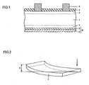
- Fig. 1 is a schematic view which shows a general sectional structure of a solar cell element.
- the solar cell element is formed using a p-type silicon semiconductor substrate 1 having a thickness of 200 to 300 ⁇ m.
- a p-type impurity layer 2 having a thickness of 0.3 to 0.6 ⁇ m is provided on the photoreceptive surface of the silicon semiconductor substrate 1.
- an antireflection film 3 and a grid electrode 4 are provided on the n-type impurity layer 2.
- a back electrode layer 5 is provided on the back surface of the p-type silicon semiconductor substrate 1.
- the back electrode layer 5 is formed by coating the p-type silicon semiconductor substrate 1 with a paste composition composed of aluminum powder, glass frit, and an organic vehicle by, for example, screen printing, and drying the paste composition, and firing the paste composition at a temperature of 660°C (i.e., the melting point of aluminum) or higher.
- a temperature of 660°C i.e., the melting point of aluminum
- aluminum is diffused into the p-type silicon semiconductor substrate 1, so that an Al-Si alloy layer 6 is formed between the back electrode layer 5 and the p-type silicon semiconductor substrate 1, and at the same time, a p + layer 7 is also formed as an impurity layer resulting from the diffusion of aluminum atoms.
- An electrode 8 is composed of the back electrode layer 5 and the Al-Si alloy layer 6.
- the back electrode layer 5 and the Al ⁇ Si alloy layer 6 may be removed with, for example, acid to form another electrode layer using, for example, a silver paste on the remaining p + layer 7 providing a BSF effect.
- a solar cell having such a structure is also in practical use.
- Patent Document 1 discloses a conductive paste composition capable of allowing a solar cell to have desired characteristics and reducing the bow of a silicon semiconductor substrate.
- This conductive paste contains an aluminum-containing organic compound in addition to aluminum powder, glass frit, and an organic vehicle.
- Patent Document 2 discloses a method for reducing the bow of a silicon semiconductor substrate by adding at least one of organic compound particles and carbon particles to a conventional paste composition to suppress the shrinkage of an aluminum electrode occurring during the firing of the paste composition.
- the organic compound particles or the carbon particles are present in a solid particle state in the paste composition, but these particles are burnt and then disappear during the firing of the paste composition, and as a result, a plurality of micro pores are formed in an obtained electrode, thereby suppressing the bow of a silicon semiconductor substrate.
- the present invention is directed to a paste composition to be used for forming an electrode on a silicon semiconductor substrate, including: aluminum powder; an organic vehicle; and whisker insoluble or hardly-soluble in the organic vehicle, wherein the whisker is previously mixed with the aluminum powder and the organic vehicle.
- the paste composition according to the present invention further includes glass frit.
- the paste composition according to the present invention contains the whisker in an amount of 0.2% by mass or more but 15.0% by mass or less.
- the paste composition according to the present invention contains the aluminum powder in an amount of 60% by mass or more but 80% by mass or less, the organic vehicle in an amount of 20% by mass or more but 40% by mass or less, and the whisker in an amount of 0.2% by mass or more but 15.0% by mass or less.
- the paste composition preferably contains the aluminum powder in an amount of 60% by mass or more but 80% by mass or less, the organic vehicle in an amount of 20% by mass or more but 40% by mass or less, the whisker in an amount of 0.2% by mass or more but 15.0% by mass or less, and the glass frit in an amount of 7.0% by mass or less.
- the whisker is preferably at least one selected from the group consisting of metals, inorganic materials, and organic materials.
- the whisker preferably has a diameter of 15 ⁇ m or less and an aspect ratio of 2 or more.
- the present invention is also directed to an electrode formed by applying a paste composition having any one of the above-described characteristics onto a silicon semiconductor substrate and then firing the paste composition.
- the present invention is also directed to a solar cell element including an electrode formed by applying a paste composition having any one of the above-described characteristics onto a silicon semiconductor substrate and then firing the paste composition.
- the use of the paste composition according to the present invention containing whisker makes it possible to reduce the deformation of the silicon semiconductor substrate occurring after the firing of the paste composition applied onto the silicon semiconductor substrate without the necessity to reduce the amount of the paste composition applied onto the silicon semiconductor substrate, so that an obtained aluminum electrode has mechanical strength and good adhesion to the silicon semiconductor substrate and therefore a desired BSF effect improving the collection efficiency for generated carriers is achieved.
- a paste composition according to the present invention is characterized by containing whisker in addition to aluminum powder and an organic vehicle.
- whisker By using such a paste composition containing whisker as a paste applied onto a silicon semiconductor substrate, it is possible to suppress the deformation of a silicon semiconductor substrate occurring after the firing of the paste composition.
- the use of the paste composition according to the present invention makes it possible to suppress the deformation of a silicon semiconductor substrate occurring after the firing of the paste composition without the necessity to reduce the thickness of a coating of the paste composition, whereby a desired BSF effect can be obtained.
- the reason why the use of the paste composition obtained by previously mixing whisker with aluminum powder and an organic vehicle makes it possible to suppress the deformation of a silicon semiconductor substrate occurring after the firing of the paste composition is not clear, but it can be considered that the amount of shrinkage of a sintered aluminum layer, formed by firing of the paste composition, occurring during cooling after firing is reduced due to the existence of the whisker.
- the whisker contained in the paste composition according to the present invention at least one selected from the group consisting of metals, inorganic materials, and organic materials can be used, as long as it is not dissolved in the organic vehicle and is not thermally decomposed during firing of the paste composition.
- the amount of the whisker contained in the paste composition according to the present invention is preferably 0.2% by mass or more but 15.0% by mass or less. If the amount of the whisker contained in the paste composition according to the present invention is less than 0.2% by mass, the effect obtained by adding the whisker is not high enough to suppress the deformation of a silicon semiconductor substrate occurring after the firing of the paste composition. On the other hand, if the amount of the whisker contained in the paste composition according to the present invention exceeds 15.0% by mass, there is a fear that the sinterability of the paste composition is adversely affected, which causes a problem that the electric resistance of a back electrode layer is increased. If the electric resistance of a back electrode layer is increased, an ohmic resistance between electrodes is increased and therefore energy generated by irradiation with solar light cannot be effectively extracted from a solar cell, thereby lowering the energy conversion efficiency of the solar cell.
- the diameter of the whisker contained in the paste composition according to the present invention is preferably 15 ⁇ m or less. If the diameter of the whisker exceeds 15 ⁇ m, the number of whiskers dispersed in a sintered aluminum layer formed by firing of the paste composition is reduced, and therefore the effect obtained by adding the whisker is not high enough to suppress the deformation of a silicon semiconductor substrate occurring after the firing of the paste composition.
- the amount of the aluminum powder contained in the paste composition according to the present invention is preferably 60% by mass or more but 80% by mass or less. If the amount of the aluminum powder contained in the paste composition according to the present invention is less than 60% by mass, there is a fear that the surface resistance of a back electrode layer formed by firing of the paste composition is increased, thereby lowering the energy conversion efficiency of a solar cell. On the other hand, if the amount of the aluminum powder contained in the paste composition according to the present invention exceeds 80% by mass, the ability of the paste composition to be applied onto a silicon semiconductor substrate by screen printing or the like is lowered.
- the organic vehicle contained in the paste composition according to the present invention can be prepared by dissolving ethyl cellulose, acrylic resin, alkyd resin, or the like in a glycol ether-based solvent, a terpineol-based solvent, or the like.
- the amount of the organic vehicle contained in the paste composition according to the present invention is preferably 20% by mass or more but 40% by mass or less. If the amount of the organic vehicle contained in the paste composition according to the present invention is less than 20% by mass or exceeds 40% by mass, printability of the paste composition is lowered.
- the paste composition according to the present invention may further contain glass frit.
- the amount of the glass frit contained in the paste composition according to the present invention is preferably 7.0% by mass or less.
- the glass frit is not directly involved in the deformation of the silicon semiconductor substrate, a BSF effect, and energy conversion efficiency, but addition of the glass frit improves the adhesion between a back electrode formed by firing of the paste composition and a silicon semiconductor substrate. If the amount of the glass frit contained in the paste composition according to the present invention exceeds 7.0% by mass, there is a fear that segregation of glass occurs.
- Examples of the glass frit contained in the paste composition according to the present invention include SiO 2 -Bi 2 O 3 -PbO-based glass frit, B 2 O 3 -SiO 2 -Bi 2 O 3 -based glass frit, B 2 0 3 -SiO 2 -ZnO-based glass frit, and B 2 O 3 -SiO 2 -PbO-based glass frit.
- ethyl cellulose was dissolved in a glycol ether-based organic solvent to prepare an organic vehicle, and aluminum powder and B 2 O 3 -SiO 2 -PbO-based glass frit were added to the organic vehicle, and then any one of whiskers shown in Table 1 was added thereto in an amount shown in Table 2.
- the thus obtained mixture was mixed using a well-known mixer to prepare a paste composition (Examples 1 to 5).
- Paste compositions of Comparative Examples 2 and 3 were also prepared in the same manner as in Examples 1 to 5 except that the whisker was replaced with any one of powders shown in Table 1 and the powder was added in an amount shown in Table 2. Further, a paste composition of Comparative Example 1 containing neither whisker nor powder shown in Table 1 was also prepared. It is to be noted that in Table 2, the symbols "W” and "P” in parenthesis in the column "Type of Additive" represent whisker and powder, respectively.
- the aluminum powder used for preparing these paste compositions was composed of spherical or nearly-spherical particles having an average particle diameter of 2 to 20 ⁇ m from the viewpoint of ensuring of reactivity with a silicon semiconductor substrate, the ability of the paste composition to be applied onto a silicon semiconductor substrate, and the uniformity of a coating of the paste composition.
- Each of the paste compositions was applied onto a p-type silicon semiconductor substrate having a thickness of 200 ⁇ m and a size of 155 mm x 155 mm by printing using a 250 mesh-screen printing plate, and then dried. It is to be noted that the amount of the paste composition applied onto the p-type silicon semiconductor substrate was so determined that an electrode obtained by firing the paste composition had a thickness of 25 to 30 ⁇ m.
- the p-type silicon semiconductor substrate having the printed paste composition was dried, and was then heated in an infrared firing furnace in an air atmosphere at a heating rate of 400°C/min and fired by keeping it at 720°C for 30 seconds. After firing, the p-type silicon semiconductor substrate was cooled to obtain a p-type silicon semiconductor substrate 1 having a back electrode layer 5 as shown in Fig. 1 .
- the p-type silicon semiconductor substrate having the back electrode layer was immersed in an aqueous hydrochloric acid solution to dissolve and remove the back electrode layer 5 and an Al-Si alloy layer 6, and then the surface resistance of the p-type silicon semiconductor substrate having a p + layer 7 formed thereon was measured using the surface resistance measuring device described above.
- the target surface resistances of the back electrode layer and the p + layer are 24.0 m ⁇ / ⁇ or less and 22.0 ⁇ / ⁇ or less, respectively.
- the deformation of the silicon semiconductor substrate occurring after the firing of the paste composition was evaluated by measuring the amount of deformation after cooling of the silicon semiconductor substrate in the following manner. As shown in Fig. 2 , the silicon semiconductor substrate was placed on a plane with the back electrode layer side up, and one of the four corners of the substrate was pressed against the plane to measure the amount of elevation "x" (including the thickness of the substrate) of another corner diagonally opposite to the corner pressed against the plane. It is to be noted that the target value of "x" is 2.0 mm or less.
- the mechanical strength and adhesion of the aluminum electrode formed on the silicon semiconductor substrate were evaluated based upon whether or not the aluminum electrode was separated from the substrate when a cellophane tape adhered to the aluminum electrode was peeled off from the aluminum electrode.
- the use of the paste composition according to the present invention containing whisker makes it possible to reduce the deformation of the silicon semiconductor substrate occurring after the firing of the paste composition applied onto the silicon semiconductor substrate without the necessity to reduce the amount of the paste composition applied onto the silicon semiconductor substrate.
- an aluminum electrode formed using the paste composition according to the present invention has mechanical strength and good adhesion to the silicon semiconductor substrate, and therefore a solar cell element having an electrode formed using the paste composition according to the present invention has a desired BSF effect improving the collection efficiency for generated carriers.
Landscapes
- Chemical & Material Sciences (AREA)
- Engineering & Computer Science (AREA)
- Chemical Kinetics & Catalysis (AREA)
- General Chemical & Material Sciences (AREA)
- Geochemistry & Mineralogy (AREA)
- Materials Engineering (AREA)
- Organic Chemistry (AREA)
- Life Sciences & Earth Sciences (AREA)
- Dispersion Chemistry (AREA)
- Ceramic Engineering (AREA)
- Crystallography & Structural Chemistry (AREA)
- Physics & Mathematics (AREA)
- Spectroscopy & Molecular Physics (AREA)
- Photovoltaic Devices (AREA)
- Conductive Materials (AREA)
- Electrodes Of Semiconductors (AREA)
- Paints Or Removers (AREA)
Abstract
Claims (9)
- Composition de pâte à utiliser pour former une électrode (8) sur un substrat semi-conducteur en silicium (1), comprenant :de la poudre d'aluminium ;un véhicule organique ; etde la trichite insoluble ou difficilement soluble dans le véhicule organique, dans laquelle la trichite est préalablement mélangée à la poudre d'aluminium et au véhicule organique.
- Composition de pâte selon la revendication 1, comprenant en outre de la fritte de verre.
- Composition de pâte selon la revendication 1, qui contient la trichite en une quantité supérieure ou égale à 0,2 % en masse mais inférieure ou égale à 15,0 % en masse.
- Composition de pâte selon la revendication 1, qui contient la poudre d'aluminium en une quantité supérieure ou égale à 60 % mais inférieure ou égale à 80 % en masse, le véhicule organique en une quantité supérieure ou égale à 20 % en masse mais inférieure ou égale à 40 % en masse, et la trichite en une quantité supérieure ou égale à 0,2 % en masse mais inférieure ou égale à 15,0 % en masse.
- Composition de pâte selon la revendication 2, qui contient la poudre d'aluminium en une quantité supérieure ou égale à 60 % en masse mais inférieure ou égale à 80 % en masse, le véhicule organique en une quantité supérieure ou égale à 20 % en masse mais inférieure ou égale à 40 % en masse, la trichite en une quantité supérieure ou égale à 0,2 % en masse mais inférieure ou égale à 15,0 % en masse, et la fritte de verre en une quantité inférieure ou égale à 7 % en masse.
- Composition de pâte selon la revendication 1, dans laquelle la trichite est au moins un élément choisi parmi le groupe constitué des métaux, des matières inorganiques et des matières organiques.
- Composition de pâte selon la revendication 1, dans laquelle la trichite présente un diamètre de 15 µm ou moins et un rapport d'aspect de 2 ou plus.
- Electrode (8) constituant une cellule solaire, laquelle électrode est formée en appliquant la composition de pâte selon la revendication 1 sur un substrat semi-conducteur en silicium (1) puis en chauffant la composition de pâte.
- Elément de cellule solaire comprenant une électrode (8) formée en appliquant la composition de pâte selon la revendication 1 sur un substrat semi-conducteur en silicium (1) puis en chauffant la composition de pâte.
Applications Claiming Priority (2)
| Application Number | Priority Date | Filing Date | Title |
|---|---|---|---|
| JP2005093339A JP2006278071A (ja) | 2005-03-29 | 2005-03-29 | ペースト組成物、電極およびそれを備えた太陽電池素子 |
| PCT/JP2006/304304 WO2006103882A1 (fr) | 2005-03-29 | 2006-03-07 | Composition de pate, electrode et dispositif de cellule solaire les comprenant |
Publications (3)
| Publication Number | Publication Date |
|---|---|
| EP1873790A1 EP1873790A1 (fr) | 2008-01-02 |
| EP1873790A4 EP1873790A4 (fr) | 2009-06-03 |
| EP1873790B1 true EP1873790B1 (fr) | 2011-09-14 |
Family
ID=37053149
Family Applications (1)
| Application Number | Title | Priority Date | Filing Date |
|---|---|---|---|
| EP06728673A Ceased EP1873790B1 (fr) | 2005-03-29 | 2006-03-07 | Composition de pate, electrode et dispositif de cellule solaire les comprenant |
Country Status (6)
| Country | Link |
|---|---|
| US (1) | US20080135097A1 (fr) |
| EP (1) | EP1873790B1 (fr) |
| JP (1) | JP2006278071A (fr) |
| CN (1) | CN101151681B (fr) |
| TW (1) | TWI401808B (fr) |
| WO (1) | WO2006103882A1 (fr) |
Families Citing this family (11)
| Publication number | Priority date | Publication date | Assignee | Title |
|---|---|---|---|---|
| JP4903531B2 (ja) * | 2006-10-30 | 2012-03-28 | 京セラ株式会社 | 太陽電池素子 |
| JP2008160018A (ja) * | 2006-12-26 | 2008-07-10 | Toyo Aluminium Kk | ペースト組成物およびそれを用いた太陽電池素子 |
| EP2143146A1 (fr) * | 2007-04-13 | 2010-01-13 | Semiconductor Energy Laboratory Co, Ltd. | Dispositif photovoltaique et son procede de fabrication |
| JP2008306023A (ja) * | 2007-06-08 | 2008-12-18 | Toyo Aluminium Kk | ペースト組成物と太陽電池素子 |
| JP4443597B2 (ja) | 2007-11-19 | 2010-03-31 | セイコーエプソン株式会社 | 表示装置、表示装置の製造方法および電子機器 |
| JP5160321B2 (ja) * | 2008-06-27 | 2013-03-13 | 株式会社ノリタケカンパニーリミテド | シリコン系太陽電池の製造方法および該製造方法に用いるアルミニウムペースト |
| JP5410242B2 (ja) * | 2009-03-31 | 2014-02-05 | 積水化学工業株式会社 | 導電性微粒子分散ペースト |
| CN102142467B (zh) * | 2010-01-29 | 2013-07-03 | 比亚迪股份有限公司 | 一种太阳电池背电场铝浆及其制备方法 |
| KR101181190B1 (ko) * | 2010-07-30 | 2012-09-18 | 엘지이노텍 주식회사 | 태양 전지 및 이의 후면 전극용 페이스트 조성물 |
| WO2012044281A1 (fr) * | 2010-09-28 | 2012-04-05 | E. I. Du Pont De Nemours And Company | Pâte conductrice pour électrode de cellule solaire |
| JP2012107206A (ja) * | 2010-10-26 | 2012-06-07 | Daicel Corp | 印刷用溶剤又は溶剤組成物 |
Family Cites Families (16)
| Publication number | Priority date | Publication date | Assignee | Title |
|---|---|---|---|---|
| JPS6194391A (ja) * | 1984-10-15 | 1986-05-13 | アルプス電気株式会社 | 回路形成用の導電ペ−スト |
| JPS6315866A (ja) * | 1986-07-07 | 1988-01-22 | Copal Co Ltd | 厚膜ペ−スト用導電性組成物 |
| JPH0418703A (ja) * | 1990-05-11 | 1992-01-22 | Nippon Teikouki Seisakusho:Kk | 摺動用抵抗ペースト |
| JPH0511265A (ja) * | 1991-07-08 | 1993-01-19 | Koufu Kashio Kk | 異方性導電膜 |
| JP3223199B2 (ja) * | 1991-10-25 | 2001-10-29 | ティーディーケイ株式会社 | 多層セラミック部品の製造方法および多層セラミック部品 |
| JP2716641B2 (ja) * | 1992-12-28 | 1998-02-18 | キヤノン株式会社 | 光起電力素子の集電電極及びその製造方法 |
| JPH06333417A (ja) * | 1993-05-21 | 1994-12-02 | Hitachi Chem Co Ltd | 導電ペースト |
| JP2000090733A (ja) * | 1998-09-14 | 2000-03-31 | Murata Mfg Co Ltd | 導電性ペースト及びそれを用いた太陽電池 |
| JP2000090734A (ja) * | 1998-09-16 | 2000-03-31 | Murata Mfg Co Ltd | 導電性ペースト及びそれを用いた太陽電池 |
| TWI285671B (en) * | 1998-10-13 | 2007-08-21 | Orion 21 A D Pty Ltd | Luminescent gel coats and moldable resins |
| JP2000119518A (ja) * | 1998-10-15 | 2000-04-25 | Hitachi Ltd | 硬化性樹脂組成物及び耐熱性樹脂組成物並びに導電性ペースト |
| US6649824B1 (en) * | 1999-09-22 | 2003-11-18 | Canon Kabushiki Kaisha | Photoelectric conversion device and method of production thereof |
| JP4636644B2 (ja) * | 2000-01-17 | 2011-02-23 | 富士フイルム株式会社 | 電解質組成物、電気化学電池およびイオン性液晶モノマー |
| JP3910072B2 (ja) * | 2002-01-30 | 2007-04-25 | 東洋アルミニウム株式会社 | ペースト組成物およびそれを用いた太陽電池 |
| JP2004051755A (ja) * | 2002-07-18 | 2004-02-19 | Ricoh Co Ltd | 弾性導電樹脂及び弾性導電接合構造 |
| US20040055635A1 (en) * | 2002-09-19 | 2004-03-25 | Hiroshi Nagakubo | Conductive paste, method for manufacturing solar battery, and solar battery |
-
2005
- 2005-03-29 JP JP2005093339A patent/JP2006278071A/ja active Pending
-
2006
- 2006-03-07 EP EP06728673A patent/EP1873790B1/fr not_active Ceased
- 2006-03-07 CN CN2006800104292A patent/CN101151681B/zh not_active Expired - Fee Related
- 2006-03-07 US US11/883,959 patent/US20080135097A1/en not_active Abandoned
- 2006-03-07 WO PCT/JP2006/304304 patent/WO2006103882A1/fr not_active Ceased
- 2006-03-24 TW TW095110259A patent/TWI401808B/zh not_active IP Right Cessation
Also Published As
| Publication number | Publication date |
|---|---|
| CN101151681B (zh) | 2011-03-30 |
| TW200644266A (en) | 2006-12-16 |
| US20080135097A1 (en) | 2008-06-12 |
| EP1873790A4 (fr) | 2009-06-03 |
| WO2006103882A1 (fr) | 2006-10-05 |
| EP1873790A1 (fr) | 2008-01-02 |
| JP2006278071A (ja) | 2006-10-12 |
| TWI401808B (zh) | 2013-07-11 |
| CN101151681A (zh) | 2008-03-26 |
Similar Documents
| Publication | Publication Date | Title |
|---|---|---|
| US7368657B2 (en) | Paste composition and solar cell employing the same | |
| JP4802097B2 (ja) | ペースト組成物およびそれを用いた太陽電池素子 | |
| KR100798255B1 (ko) | 전기전도성 후막 조성물, 이로부터 형성된 전극 및 태양전지 | |
| EP2417609B1 (fr) | Pâte et pile solaire utilisant celle-ci | |
| WO2010124161A1 (fr) | Pâtes métalliques et utilisation de celles-ci dans la fabrication d'électrodes positives sur des surfaces de silicium de type p | |
| CN102473756A (zh) | 糊组合物及使用其的太阳能电池元件 | |
| EP1873790B1 (fr) | Composition de pate, electrode et dispositif de cellule solaire les comprenant | |
| CN101292364A (zh) | 铝膏组合物和使用了它的太阳电池元件 | |
| EP1939943B1 (fr) | Composition en pate et element de batterie de piles solaires l'utilisant | |
| US8197718B2 (en) | Paste composition and solar cell element using the same | |
| US8741167B1 (en) | Etching composition and its use in a method of making a photovoltaic cell | |
| EP2383794A1 (fr) | Composition de pâte et élément de cellule solaire l'utilisant | |
| KR20110048403A (ko) | 도전성 페이스트 및 이를 이용한 태양전지 전극 | |
| JP2005317898A (ja) | ペースト組成物およびそれを用いた太陽電池素子 | |
| JP2002141520A (ja) | 太陽電池素子およびその製造方法 | |
| KR20170098596A (ko) | 비히클 기화 완화제가 첨가된 태양전지 전극용 페이스트 조성물 및 이를 이용하여 제조된 태양전지 | |
| CN103907207A (zh) | 形成半导体基板的p型掺杂铝表面区域的方法 |
Legal Events
| Date | Code | Title | Description |
|---|---|---|---|
| PUAI | Public reference made under article 153(3) epc to a published international application that has entered the european phase |
Free format text: ORIGINAL CODE: 0009012 |
|
| 17P | Request for examination filed |
Effective date: 20070927 |
|
| AK | Designated contracting states |
Kind code of ref document: A1 Designated state(s): DE |
|
| DAX | Request for extension of the european patent (deleted) | ||
| RBV | Designated contracting states (corrected) |
Designated state(s): DE |
|
| A4 | Supplementary search report drawn up and despatched |
Effective date: 20090508 |
|
| 17Q | First examination report despatched |
Effective date: 20090715 |
|
| GRAP | Despatch of communication of intention to grant a patent |
Free format text: ORIGINAL CODE: EPIDOSNIGR1 |
|
| GRAS | Grant fee paid |
Free format text: ORIGINAL CODE: EPIDOSNIGR3 |
|
| GRAA | (expected) grant |
Free format text: ORIGINAL CODE: 0009210 |
|
| AK | Designated contracting states |
Kind code of ref document: B1 Designated state(s): DE |
|
| REG | Reference to a national code |
Ref country code: DE Ref legal event code: R096 Ref document number: 602006024379 Country of ref document: DE Effective date: 20111117 |
|
| PLBE | No opposition filed within time limit |
Free format text: ORIGINAL CODE: 0009261 |
|
| STAA | Information on the status of an ep patent application or granted ep patent |
Free format text: STATUS: NO OPPOSITION FILED WITHIN TIME LIMIT |
|
| 26N | No opposition filed |
Effective date: 20120615 |
|
| REG | Reference to a national code |
Ref country code: DE Ref legal event code: R097 Ref document number: 602006024379 Country of ref document: DE Effective date: 20120615 |
|
| PGFP | Annual fee paid to national office [announced via postgrant information from national office to epo] |
Ref country code: DE Payment date: 20190219 Year of fee payment: 14 |
|
| REG | Reference to a national code |
Ref country code: DE Ref legal event code: R119 Ref document number: 602006024379 Country of ref document: DE |
|
| PG25 | Lapsed in a contracting state [announced via postgrant information from national office to epo] |
Ref country code: DE Free format text: LAPSE BECAUSE OF NON-PAYMENT OF DUE FEES Effective date: 20201001 |