EP1890326A2 - Structure comprenant un substrat avec un CI intégré dans le substrat et un support, et procédé de fabrication d'une telle structure - Google Patents
Structure comprenant un substrat avec un CI intégré dans le substrat et un support, et procédé de fabrication d'une telle structure Download PDFInfo
- Publication number
- EP1890326A2 EP1890326A2 EP07013966A EP07013966A EP1890326A2 EP 1890326 A2 EP1890326 A2 EP 1890326A2 EP 07013966 A EP07013966 A EP 07013966A EP 07013966 A EP07013966 A EP 07013966A EP 1890326 A2 EP1890326 A2 EP 1890326A2
- Authority
- EP
- European Patent Office
- Prior art keywords
- carrier
- adhesion
- integrated substrate
- interface
- specific area
- Prior art date
- Legal status (The legal status is an assumption and is not a legal conclusion. Google has not performed a legal analysis and makes no representation as to the accuracy of the status listed.)
- Withdrawn
Links
Images


Classifications
-
- H—ELECTRICITY
- H10—SEMICONDUCTOR DEVICES; ELECTRIC SOLID-STATE DEVICES NOT OTHERWISE PROVIDED FOR
- H10P—GENERIC PROCESSES OR APPARATUS FOR THE MANUFACTURE OR TREATMENT OF DEVICES COVERED BY CLASS H10
- H10P95/00—Generic processes or apparatus for manufacture or treatments not covered by the other groups of this subclass
- H10P95/11—Separation of active layers from substrates
-
- H—ELECTRICITY
- H10—SEMICONDUCTOR DEVICES; ELECTRIC SOLID-STATE DEVICES NOT OTHERWISE PROVIDED FOR
- H10D—INORGANIC ELECTRIC SEMICONDUCTOR DEVICES
- H10D30/00—Field-effect transistors [FET]
- H10D30/60—Insulated-gate field-effect transistors [IGFET]
- H10D30/67—Thin-film transistors [TFT]
- H10D30/6758—Thin-film transistors [TFT] characterised by the insulating substrates
-
- H—ELECTRICITY
- H10—SEMICONDUCTOR DEVICES; ELECTRIC SOLID-STATE DEVICES NOT OTHERWISE PROVIDED FOR
- H10P—GENERIC PROCESSES OR APPARATUS FOR THE MANUFACTURE OR TREATMENT OF DEVICES COVERED BY CLASS H10
- H10P72/00—Handling or holding of wafers, substrates or devices during manufacture or treatment thereof
- H10P72/70—Handling or holding of wafers, substrates or devices during manufacture or treatment thereof for supporting or gripping
- H10P72/74—Handling or holding of wafers, substrates or devices during manufacture or treatment thereof for supporting or gripping using temporarily an auxiliary support
- H10P72/7402—Wafer tapes, e.g. grinding or dicing support tapes
-
- H—ELECTRICITY
- H10—SEMICONDUCTOR DEVICES; ELECTRIC SOLID-STATE DEVICES NOT OTHERWISE PROVIDED FOR
- H10W—GENERIC PACKAGES, INTERCONNECTIONS, CONNECTORS OR OTHER CONSTRUCTIONAL DETAILS OF DEVICES COVERED BY CLASS H10
- H10W70/00—Package substrates; Interposers; Redistribution layers [RDL]
- H10W70/01—Manufacture or treatment
- H10W70/05—Manufacture or treatment of insulating or insulated package substrates, or of interposers, or of redistribution layers
-
- H—ELECTRICITY
- H10—SEMICONDUCTOR DEVICES; ELECTRIC SOLID-STATE DEVICES NOT OTHERWISE PROVIDED FOR
- H10P—GENERIC PROCESSES OR APPARATUS FOR THE MANUFACTURE OR TREATMENT OF DEVICES COVERED BY CLASS H10
- H10P72/00—Handling or holding of wafers, substrates or devices during manufacture or treatment thereof
- H10P72/70—Handling or holding of wafers, substrates or devices during manufacture or treatment thereof for supporting or gripping
- H10P72/74—Handling or holding of wafers, substrates or devices during manufacture or treatment thereof for supporting or gripping using temporarily an auxiliary support
- H10P72/7416—Handling or holding of wafers, substrates or devices during manufacture or treatment thereof for supporting or gripping using temporarily an auxiliary support used during dicing or grinding
-
- H—ELECTRICITY
- H10—SEMICONDUCTOR DEVICES; ELECTRIC SOLID-STATE DEVICES NOT OTHERWISE PROVIDED FOR
- H10P—GENERIC PROCESSES OR APPARATUS FOR THE MANUFACTURE OR TREATMENT OF DEVICES COVERED BY CLASS H10
- H10P72/00—Handling or holding of wafers, substrates or devices during manufacture or treatment thereof
- H10P72/70—Handling or holding of wafers, substrates or devices during manufacture or treatment thereof for supporting or gripping
- H10P72/74—Handling or holding of wafers, substrates or devices during manufacture or treatment thereof for supporting or gripping using temporarily an auxiliary support
- H10P72/7424—Handling or holding of wafers, substrates or devices during manufacture or treatment thereof for supporting or gripping using temporarily an auxiliary support used as a support during the manufacture of self-supporting substrates
-
- H—ELECTRICITY
- H10—SEMICONDUCTOR DEVICES; ELECTRIC SOLID-STATE DEVICES NOT OTHERWISE PROVIDED FOR
- H10P—GENERIC PROCESSES OR APPARATUS FOR THE MANUFACTURE OR TREATMENT OF DEVICES COVERED BY CLASS H10
- H10P72/00—Handling or holding of wafers, substrates or devices during manufacture or treatment thereof
- H10P72/70—Handling or holding of wafers, substrates or devices during manufacture or treatment thereof for supporting or gripping
- H10P72/74—Handling or holding of wafers, substrates or devices during manufacture or treatment thereof for supporting or gripping using temporarily an auxiliary support
- H10P72/7426—Handling or holding of wafers, substrates or devices during manufacture or treatment thereof for supporting or gripping using temporarily an auxiliary support used as a support during build up manufacturing of active devices
Definitions
- the invention relates to a structure combining an IC integrated substrate and a carrier fabricated by an adhesion-differentiating process, a method of manufacturing such structure, and a method of manufacturing an electronic device using such structure.
- the line width, line spacing, and size of chips become smaller and smaller, and the chips require faster transmission speed.
- better packaging technology for electrically connecting the chips to the exterior is required to increase the wiring density. Therefore, the chip packaging technology transformed from through hole type to surface mount type, the lead frame went from connecting by gold wire to using bumps, and circuit boards started out from hard printed circuit boards (PCB) to flexible printed circuit boards (FPCB) and to multilayer thin-film substrates.
- PCB hard printed circuit boards
- FPCB flexible printed circuit boards
- a typical six-layer PCB with BT material weighs about 4 grams and has a thickness of about 1 mm, and thus it cannot be bent.
- An FPCB with a thickness of about 50 ⁇ m can only be made with two layers of interconnection.
- a multilayer thin-film substrate with a thickness of about 50 ⁇ m can have six layers of interconnection and weighs about 0.21 grams in total, and therefore the multilayer thin-film substrate has the best flexibility and is the most compact.
- the minimum diameter of through holes is 50 ⁇ m
- the minimum dimension of through hole bonding pads is 100 ⁇ m
- the minimum line width and line spacing are 25 ⁇ m
- the minimum diameter of through holes is 20 ⁇ m
- the minimum dimension of through hole bonding pads is 25 ⁇ m
- the minimum line width and line spacing are 20 ⁇ m
- the multilayer thin-film substrate greatly increases the interconnection density.
- the multilayer thin-film substrate due to its flexibility, is especially suitable for products that have special limitation in size or have a structure with bending design.
- the aforementioned multilayer thin-film substrate is used as an IC packaging substrate, playing a conventional role of electrical signal transmission and interface connection.
- the multilayer thin-film substrate technology has a larger room for growth because semiconductor devices with functionalities can be formed on the multilayer thin-film substrate, and thereby can greatly enhance its functionality.
- the semiconductor device can be, for example, passive devices, driver ICs, and thin film transistors (TFT).
- TFT thin film transistors
- a key to manufacturing an IC integrated substrate is the size stability of the IC integrated substrate in the manufacturing process.
- a conventional solution is to manufacture the IC integrated substrate on a rigid carrier, in which the size stability of the carrier is used to increase the size stability of the IC integrate substrate during processing.
- a major issue of using this solution is the separation of the IC integrated substrate and the carrier after the fabrication of the IC integrated substrate is completed.
- U.S. patent No. 4480288 a double-sided thin, flexible circuitry is formed on an aluminum carrier, and then the aluminum carrier is removed by hydrochloric acid.
- U.S. Patent No. 4812191 discloses a method of manufacturing a multilayer thin-film substrate comprising a multilayer interconnection structure by using a sacrificial substrate technique.
- a multilayer interconnection structure is formed on a carrier that has a coefficient of thermal expansion less than that of the structure, and then the temperature is elevated to perform curing, after which the temperature is lowered to generate sufficient tension between the carrier and the multilayer interconnection structure.
- the multilayer interconnection structure is separated from the carrier by adhering a support means to the multi-layer interconnection structure and by an acid-etching process.
- U.S. Patent No. 5258236 is about a method of separating a carrier and a multilayer thin-film substrate having a multilayer interconnection structure by laser ablation.
- a polymer layer 2, a metal layer 3, and a multilayer interconnection structure 4 are sequentially formed on a transparent carrier 1.
- Ultraviolet light is then applied to the polymer layer 2 through the transparent carrier 1 in order to ablate the polymer 2, allowing the transparent carrier 1 to be separated from the rest of the structure.
- a structure combining an IC integrated substrate and a carrier comprises a carrier and an IC integrated substrate formed on the carrier.
- An interface between the carrier and the IC integrated substrate has a specific area at which the interface adhesion is different from that at remaining area of the interface.
- a method of manufacturing a structure combining an IC integrated substrate and a carrier comprises providing a carrier; performing an adhesion-differentiating process on the carrier; and forming an IC integrated substrate on the carrier.
- An interface between the carrier being treated by the adhesion-differentiating process and the IC integrated substrate has a specific area at which the interface adhesion is different from that at remaining area of the interface.
- a method of manufacturing an electronic device comprises providing a carrier; performing an adhesion-differentiating process on the carrier; forming an IC integrated substrate on the carrier, wherein an interface between the carrier being treated by the adhesion-differentiating process and the IC integrated substrate has a specific area at which the interface adhesion is different from that at remaining area of the interface; and cutting one or more pieces from the IC integrated substrate, so that each piece cut from the IC integrated substrate naturally separates from the carrier to obtain an electronic device.
- the IC integrated substrate mentioned in the invention is different from the multilayer thin-film substrate used in conventional packaging process.
- the IC integrated substrate of the invention can have a multilayer interconnection structure for electrical connection, or at least one semiconductor device such as passive devices, electronic drivers, TFT devices, other electronic devices, or any combination thereof.
- the IC integrated substrate and the carrier can be separated, according to the invention, by an easy, fast, and low-cost way in comparison to the conventional technology wherein complex methods like solvent and laser are used to separate a multilayer thin-film substrate and a carrier.
- An electronic device comprising a multilayer interconnection structure, at least one semiconductor device, or a combination thereof is thus manufactured.
- FIG. 1 shows a conventional method of separating an electronic device from a carrier by laser ablation.
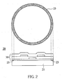
- FIG. 2 schematically shows a structure combining an IC integrated substrate having at least one semiconductor device and a carrier according to an embodiment of the invention.
- FIG. 3 shows a method of manufacturing the structure in FIG. 2 and an electronic device according to an embodiment of the invention.
- FIG. 4 schematically shows a structure combining an IC integrated substrate having a multi-layer interconnection structure and a carrier according to another embodiment of the invention.
- FIG. 5 shows the specific area with different interface adhesion from the other area in a form of grids.
- FIG. 6 shows the specific area with different interface adhesion from the other area in a form of spots.
- FIG. 2 schematically shows a structure 20 combining an IC integrated substrate 30 and a carrier 21 according to an embodiment of the invention.
- the upper portion of FIG. 2 illustrates a top view of the whole structure and the lower portion illustrates its cross-sectional view.
- the structure 20 comprises a carrier 21 and an IC integrated substrate 30 formed on the carrier 21, and the interface between the carrier 21 and the IC integrated substrate 30 has a specific area (e.g. the peripheral region 23 in this embodiment), at which the interface adhesion is different from that at remaining area of the interface.
- the interface adhesion at the peripheral region 23 can be stronger than that at the remaining area.
- the IC integrated substrate 30 of this embodiment includes at least one semiconductor device such as passive devices, driver ICs, TFT devices, or other electronic devices. It should be noted that in FIG. 2, the IC integrated substrate 30 contains a single semiconductor device, but a person skilled in the art should know that an IC integrated substrate may contain a lot of semiconductor devices, and can be cut in subsequent procedures to make hundreds and thousands of electronic devices. The simplification herein is for easy illustration and description purposes.
- the carrier 21 is provided in FIG. 3A.
- the carrier 21 is treated by an adhesion-differentiating process, and then a bottom dielectric layer 31 of the IC integrated substrate 30 is formed on the carrier 21, so that the interface adhesion at the peripheral region 23 is stronger than that at the remaining area on the interface between the carrier 21 and the bottom dielectric layer 31.
- the adhesion-differentiating process the carrier 21 and the bottom dielectric layer 31 are substantially adhered together merely in the peripheral region 23, but substantially non-adhered in the other area.
- the term "substantially adhered” means a condition that two contact surfaces are attached to each other firmly and would not be separated due to the stress produced during the subsequent processes
- the term “substantially non-adhered” means a state that interface adhesion between two contact surfaces is so weak that the two surfaces can be naturally separated, namely, they can be separated by applying little external force (e.g. by vacuum suction or tape sticking etc.) without damage to their structures.
- the so-called “adhesion differentiating process” in the invention means a process that can regionally differentiate the adhesion on the interface between the carrier and the IC integrated substrate, and its procedures depend on the materials of the carrier and the bottom layer of the IC integrated substrate.
- the adhesion-differentiating process may comprise performing an adhesion promoting treatment on some areas of the carrier, performing an adhesion reducing treatment on some areas of the carrier, performing an adhesion promoting treatment on the whole carrier and then performing an adhesion reducing treatment on some areas, or performing an adhesion reducing treatment on the whole carrier and then performing an adhesion promoting treatment on some areas.
- the material of the carrier 21 is a silicon wafer
- the material of the bottom dielectric layer 31 is polyimide (DuPont PI-2611) with a low dielectric constant (less than 4). Since the adhesion between these two materials is very weak (i.e. "substantially non-adhered"), the adhesion-differentiating process in this embodiment merely comprises performing an adhesion promoting treatment on the peripheral region 23. Specifically, a silane-based adhesion promoter (DuPont VM-651) is applied to the peripheral region 23 of the carrier 21 to enhance the adhesion between the carrier 21 and the bottom dielectric layer 31, and the remaining area of the carrier 21 is untreated. After spin-coated on the carrier 21, the bottom dielectric layer 31 is substantially adhered to the carrier 21 in the peripheral region 23.
- a silane-based adhesion promoter DuPont VM-651
- FIG. 3C other components of a semiconductor such as a gate electrode 32, a source electrode 33, a drain electrode 34, a dielectric layer 35, and a semiconductor layer 36 etc. are formed on the bottom dielectric layer 31 to complete the IC integrated substrate 30 having a semiconductor device.
- FIG. 3D the IC integrated substrate 30 is cut into one or more pieces at some proper positions. Since the IC integrated substrate 30 (the bottom dielectric layer 31) and the carrier 21 are substantially adhered together in the peripheral region 23, but substantially non-adhered in the other area, each piece cut from the IC integrated substrate 30 can be naturally separated from the carrier 21 to obtain an electronic device 38, for example, by vacuum suction.
- an electronic device having at least one semiconductor device with high size accuracy and excellent flexibility can be manufactured more easily and faster in this embodiment.
- FIG. 4 schematically shows a structure 40 combining an IC integrated substrate 50 and a carrier 41 according to another embodiment of the invention.
- the structure 40 comprises a carrier 41 and an IC integrated substrate 50 formed on the carrier 41, and on the interface between them, the adhesion at the peripheral region 43 is stronger than that at the remaining area.
- the IC integrated substrate 50 has a multi-layer interconnection structure, which is a double-sided substrate with both its front side and back side electrically connected to the exterior. Inside this double-sided substrate, the front side electrically connects to the back side, but the multi-layer interconnection structure can be interconnected by other methods, such as interconnecting in multiple places on one surface, or in other conditions.
- the number of layers in the multi-layer interconnection structure is unlimited, and it can be appropriately adjusted according to different applications.
- a silicon wafer is used as the carrier 41, and the IC integrated substrate 50 having a multi-layer interconnection structure is formed by sequentially laminating dielectric layers and metal layers on the carrier 41, wherein each of the dielectric layers 51, 53, 55, and 57 is made of polyimide (DuPont PI-2611) with a low dielectric constant (less than 4); the upper metal layer 56 and the lower metal layer 52 are under bump metal (UBM) with Cr/Cu/Ni/Au structure for subsequent electrical connection to solder balls; and the middle metal layer 54 is multi-layer metal wires of Cr/Cu/Cr.
- the dielectric layers 53, 55, and 57 of the multi-layer interconnection structure can be perforated by etching or laser drilling so that the metal interconnections can electrically connect to one another, or to the exterior.
- the adhesion-differentiating process in this embodiment merely comprises performing an adhesion promoting treatment on the peripheral region 43. Its procedures are the same as those in FIG. 3, and not described herein for simplification. After the adhesion-differentiating process and the spin coating process, the dielectric layer 51 is substantially adhered to the carrier 41 only in the peripheral region 43.
- the metal layer 52, the dielectric layer 53, the metal layer 54, the dielectric layer 55, the metal layer 56, and the dielectric layer 57 are sequentially stacked on the dielectric layer 51 to form the IC integrated substrate 50.
- the IC integrated substrate 50 is cut into one or more pieces at some proper positions. Since the IC integrated substrate 50 (the dielectric layer 51) and the carrier 41 are substantially adhered together in the peripheral region 43, but substantially non-adhered in the other area, each piece cut from the IC integrated substrate 50 can be naturally separated from the carrier 41 to obtain an electronic device, for example, by vacuum suction.
- an electronic device having a multi-layer interconnection structure with high size accuracy and excellent flexibility can be manufactured more easily and faster in this embodiment.
- the carrier in the invention can be all types of solid material, including metal, glass, ceramic, silicon wafer, sapphire, gallium arsenide, polyimide (PI), etc.
- the dielectric layers can be any organic material, including PI, benzo-cyclobutene (BCB), poly(methyl-methacrylate) (PMMA), liquid crystal polymer (LCP), etc.
- the procedures of the adhesion-differentiating process in the invention may be properly adjusted in the light of the above materials.
- it comprises performing an adhesion promoting treatment on a specific area of the carrier, which can be achieved by using the original characteristic of the carrier, or by methods of enhancing surface energy like plasma treatment, or by using material that enhances the interaction and crosslink between interface particles, such as a silane-based promoter.
- Table 1 illustrates examples of various methods of adhesion promoting treatment that can be selected for different materials of the carrier and the dielectric layer; however, the method is not limited thereto.
- the adhesion-differentiating process comprises performing an adhesion promoting treatment on the whole carrier and then performing an adhesion reducing treatment on a specific area.
- the adhesion promoting treatment can be achieved by coating PI on the whole carrier and then performing Ar plasma treatment on the whole carrier.
- a silane-based material e.g. DuPont VM-651
- the dielectric layer is coated on the carrier.
- the silane-based material can reduce the interface adhesion between PI and PI, the adhesion at the specific area applied with the promoter is weakened (i.e. adhesion reducing treatment).
- the adhesion-differentiating process comprises performing an adhesion reducing treatment on a specific area.
- a specific area For example, if the materials of the carrier and the dielectric layer are silicon and PI respectively, PI is firstly applied on the specific area of the carrier by ink jetting or dispensing, and then the dielectric layer containing a silane-based material (e.g. DuPont VM-651) is coated on the carrier.
- the dielectric layer contains the silane-based adhesion promoter and the specific area is applied with PI, the adhesion at the specific area is weakened (i.e. adhesion reducing treatment).
- the interface adhesion at the other area between the carrier and the dielectric layer can be enhanced by the silane-based material.
- the aforementioned embodiments are merely exemplary, but not limitative.
- the purpose of the "adhesion differentiating process" in the invention is to regionally differentiate the adhesion on the interface between the carrier and the IC integrated substrate, and its procedures can be properly modified according to the needs of different processes.
- the interface adhesion between the carrier and the IC integrated substrate can be controlled by referring to the adhesion theory recited in the following references:
- the material of a dielectric layer formed by coating can be selected based on the wetting principle, where the final adhesion is stronger when the S value is larger and the final adhesion is weaker when the S value is smaller. Based on the principle, surface treatment can be used to suitably change free energy, and thus enhance or diminish the adhesiveness of the layer, to achieve the adhesion result required by the invention. Because the actual value of the adhesion is greatly affected by process quality, persons skilled in the art should understand that the principle is a qualitative result and that the actual S value is not to be used for specific applications. However, by trial and error, a suitable adhesion between the carrier and the dielectric layer in the invention can be obtained, and thus the effect of natural separation as suggested by the invention can be achieved.
- the wetting principle also applies to dielectric layers formed by non-coating methods like lamination and cold forging because plastic flow would form at the microscopic contact points of these methods. And since the product of the invention must be solid, it naturally conforms to the solidification principle.
- Dielectric layers formed by non-coating methods also need to fully consider the deformation principle. If the contact surface can completely deform during processing, the adhesion would be stronger, otherwise it would be weaker. By appropriately utilizing these principles, the natural separation effect of the invention can be achieved.
- the specific area, at which the interface adhesion is different from the other area is located at the periphery of the carrier, but it can be in other locations and in any shape, such as in grids or spots, so long as defects like bubbling or delamination do not occur in subsequent processes.
- FIGs. 5 and 6 show the specific area in a form of grids and in a form of spots respectively.
Landscapes
- Thin Film Transistor (AREA)
- Internal Circuitry In Semiconductor Integrated Circuit Devices (AREA)
- Structures Or Materials For Encapsulating Or Coating Semiconductor Devices Or Solid State Devices (AREA)
Applications Claiming Priority (1)
| Application Number | Priority Date | Filing Date | Title |
|---|---|---|---|
| CN200610115525.5A CN101127343B (zh) | 2006-08-18 | 2006-08-18 | 结合ic整合基板与载板的结构及其制造方法与电子装置的制造方法 |
Publications (2)
| Publication Number | Publication Date |
|---|---|
| EP1890326A2 true EP1890326A2 (fr) | 2008-02-20 |
| EP1890326A3 EP1890326A3 (fr) | 2009-10-21 |
Family
ID=38708966
Family Applications (1)
| Application Number | Title | Priority Date | Filing Date |
|---|---|---|---|
| EP07013966A Withdrawn EP1890326A3 (fr) | 2006-08-18 | 2007-07-17 | Structure comprenant un substrat avec un CI intégré dans le substrat et un support, et procédé de fabrication d'une telle structure |
Country Status (2)
| Country | Link |
|---|---|
| EP (1) | EP1890326A3 (fr) |
| CN (1) | CN101127343B (fr) |
Cited By (11)
| Publication number | Priority date | Publication date | Assignee | Title |
|---|---|---|---|---|
| GB2479081A (en) * | 2009-10-21 | 2011-09-28 | Lg Display Co Ltd | Display device having plastics substrate formed on carrier substrate with adhesive adjusting layer |
| WO2011138232A1 (fr) * | 2010-05-04 | 2011-11-10 | Cicor Management AG | Procédé pour la production d'une configuration de circuit flexible |
| US8445300B2 (en) | 2009-10-21 | 2013-05-21 | Lg Display Co., Ltd. | Method of fabricating display device using plastic substrate |
| JP2013535093A (ja) * | 2010-05-20 | 2013-09-09 | エーファウ・グループ・エー・タルナー・ゲーエムベーハー | チップスタックを製造するための方法及びその方法を実施するためのキャリア |
| EP2419929A4 (fr) * | 2009-04-14 | 2014-09-24 | Int Test Solutions Inc | Appareil de nettoyage de fabrication de plaquette, processus et procédé d'utilisation |
| JP2014183270A (ja) * | 2013-03-21 | 2014-09-29 | Toshiba Corp | 半導体装置の製造方法 |
| DE102012102131B4 (de) * | 2011-03-18 | 2017-08-31 | Eternal Materials Co., Ltd. | Verfahren zur Herstellung eines flexiblen Bauelements und ein Verfahren zum Abtrennen eines flexiblen Substrates von einem starren Träger |
| US11155428B2 (en) | 2018-02-23 | 2021-10-26 | International Test Solutions, Llc | Material and hardware to automatically clean flexible electronic web rolls |
| US11211242B2 (en) | 2019-11-14 | 2021-12-28 | International Test Solutions, Llc | System and method for cleaning contact elements and support hardware using functionalized surface microfeatures |
| US11318550B2 (en) | 2019-11-14 | 2022-05-03 | International Test Solutions, Llc | System and method for cleaning wire bonding machines using functionalized surface microfeatures |
| US11756811B2 (en) | 2019-07-02 | 2023-09-12 | International Test Solutions, Llc | Pick and place machine cleaning system and method |
Families Citing this family (3)
| Publication number | Priority date | Publication date | Assignee | Title |
|---|---|---|---|---|
| CN102637575B (zh) * | 2011-02-09 | 2015-07-01 | 群康科技(深圳)有限公司 | 元件基板的制造方法 |
| CN105336682A (zh) * | 2014-08-06 | 2016-02-17 | 上海和辉光电有限公司 | 一种柔性基板的制作方法、固定方法以及固定结构 |
| CN104916550A (zh) * | 2015-06-09 | 2015-09-16 | 深圳市华星光电技术有限公司 | 用于制造柔性基板的方法以及基板结构 |
Family Cites Families (7)
| Publication number | Priority date | Publication date | Assignee | Title |
|---|---|---|---|---|
| US6391220B1 (en) * | 1999-08-18 | 2002-05-21 | Fujitsu Limited, Inc. | Methods for fabricating flexible circuit structures |
| US6214733B1 (en) * | 1999-11-17 | 2001-04-10 | Elo Technologies, Inc. | Process for lift off and handling of thin film materials |
| US6794273B2 (en) * | 2002-05-24 | 2004-09-21 | Fujitsu Limited | Semiconductor device and manufacturing method thereof |
| JP4107417B2 (ja) * | 2002-10-15 | 2008-06-25 | 日東電工株式会社 | チップ状ワークの固定方法 |
| JP2004186324A (ja) * | 2002-12-02 | 2004-07-02 | Sony Chem Corp | フレキシブル配線回路基板の製造方法 |
| JP2005303158A (ja) * | 2004-04-15 | 2005-10-27 | Nec Corp | デバイスの形成方法 |
| EP1801870A1 (fr) * | 2005-12-22 | 2007-06-27 | Princo Corp. | Substrat temporaire partiellement adhérent et sa méthode d'utilisation |
-
2006
- 2006-08-18 CN CN200610115525.5A patent/CN101127343B/zh active Active
-
2007
- 2007-07-17 EP EP07013966A patent/EP1890326A3/fr not_active Withdrawn
Cited By (18)
| Publication number | Priority date | Publication date | Assignee | Title |
|---|---|---|---|---|
| US9595456B2 (en) | 2009-04-14 | 2017-03-14 | International Test Solutions, Inc. | Wafer manufacturing cleaning apparatus, process and method of use |
| EP2419929A4 (fr) * | 2009-04-14 | 2014-09-24 | Int Test Solutions Inc | Appareil de nettoyage de fabrication de plaquette, processus et procédé d'utilisation |
| US8445300B2 (en) | 2009-10-21 | 2013-05-21 | Lg Display Co., Ltd. | Method of fabricating display device using plastic substrate |
| GB2479081B (en) * | 2009-10-21 | 2013-09-04 | Lg Display Co Ltd | Method of fabricating display device using plastic substrate |
| GB2479081A (en) * | 2009-10-21 | 2011-09-28 | Lg Display Co Ltd | Display device having plastics substrate formed on carrier substrate with adhesive adjusting layer |
| WO2011138232A1 (fr) * | 2010-05-04 | 2011-11-10 | Cicor Management AG | Procédé pour la production d'une configuration de circuit flexible |
| US20110274829A1 (en) * | 2010-05-04 | 2011-11-10 | Cicor Management AG | Method for producing a flexible circuit configuration |
| US8623450B2 (en) | 2010-05-04 | 2014-01-07 | Cicor Management AG | Method for producing a flexible circuit configuration |
| JP2013535093A (ja) * | 2010-05-20 | 2013-09-09 | エーファウ・グループ・エー・タルナー・ゲーエムベーハー | チップスタックを製造するための方法及びその方法を実施するためのキャリア |
| US8932910B2 (en) | 2010-05-20 | 2015-01-13 | Ev Group E. Thallner Gmbh | Method for producing chip stacks, and a carrier for carrying out the method |
| KR20160077231A (ko) * | 2010-05-20 | 2016-07-01 | 에베 그룹 에. 탈너 게엠베하 | 칩 스택 제조 방법, 및 본 방법을 실시하기 위한 캐리어 |
| DE102012102131B4 (de) * | 2011-03-18 | 2017-08-31 | Eternal Materials Co., Ltd. | Verfahren zur Herstellung eines flexiblen Bauelements und ein Verfahren zum Abtrennen eines flexiblen Substrates von einem starren Träger |
| JP2014183270A (ja) * | 2013-03-21 | 2014-09-29 | Toshiba Corp | 半導体装置の製造方法 |
| US11155428B2 (en) | 2018-02-23 | 2021-10-26 | International Test Solutions, Llc | Material and hardware to automatically clean flexible electronic web rolls |
| US11434095B2 (en) | 2018-02-23 | 2022-09-06 | International Test Solutions, Llc | Material and hardware to automatically clean flexible electronic web rolls |
| US11756811B2 (en) | 2019-07-02 | 2023-09-12 | International Test Solutions, Llc | Pick and place machine cleaning system and method |
| US11211242B2 (en) | 2019-11-14 | 2021-12-28 | International Test Solutions, Llc | System and method for cleaning contact elements and support hardware using functionalized surface microfeatures |
| US11318550B2 (en) | 2019-11-14 | 2022-05-03 | International Test Solutions, Llc | System and method for cleaning wire bonding machines using functionalized surface microfeatures |
Also Published As
| Publication number | Publication date |
|---|---|
| EP1890326A3 (fr) | 2009-10-21 |
| CN101127343A (zh) | 2008-02-20 |
| CN101127343B (zh) | 2010-12-15 |
Similar Documents
| Publication | Publication Date | Title |
|---|---|---|
| US7993973B2 (en) | Structure combining an IC integrated substrate and a carrier, and method of manufacturing such structure | |
| EP1890326A2 (fr) | Structure comprenant un substrat avec un CI intégré dans le substrat et un support, et procédé de fabrication d'une telle structure | |
| US9691698B2 (en) | Method of transferring and electrically joining a high density multilevel thin film to a circuitized and flexible organic substrate and associated devices | |
| US20090042336A1 (en) | Fabrication method of an organic substrate having embedded active-chips | |
| JP2004193497A (ja) | チップサイズパッケージおよびその製造方法 | |
| US8933386B2 (en) | Optical sensor device and method of manufacturing the same | |
| WO2019222330A2 (fr) | Substrats électroniques séparés sur un support souple ou rigide et procédés associés | |
| US7183190B2 (en) | Semiconductor device and fabrication method therefor | |
| US8288246B2 (en) | Structure combining an IC integrated substrate and a carrier, and method of manufacturing such structure | |
| EP1890323B1 (fr) | Procédé de fabrication d'un substrat avec une structure d'interconnexion multicouche par séparation du substrat d'un composant porteur | |
| US8426303B2 (en) | Manufacturing method of semiconductor device, and mounting structure thereof | |
| JP2005064203A (ja) | 多層配線基板の製造方法 | |
| KR102534816B1 (ko) | 신축성 전자 소자 및 그의 제조 방법 | |
| EP1801870A1 (fr) | Substrat temporaire partiellement adhérent et sa méthode d'utilisation | |
| US7351608B1 (en) | Method of precisely aligning components in flexible integrated circuit module | |
| KR100730763B1 (ko) | 다층 상호연결 구조를 갖는 기판 및 기판의 제조 방법 | |
| US8051557B2 (en) | Substrate with multi-layer interconnection structure and method of manufacturing the same | |
| TWI850772B (zh) | 電子裝置 | |
| CN1996582B (zh) | 包含多层内连线结构的载板及其制造、回收以及应用方法 | |
| Govaerts et al. | Assembly of ultra-thin chip packages (UTCPs) for enhanced flexibility of flexible displays | |
| TW202541278A (zh) | 電子裝置及其製造方法 | |
| KR100445296B1 (ko) | 플립 칩 온 필름 및 그 제조방법 | |
| KR20060069781A (ko) | 플립 칩 온 필름 및 그 제조방법 | |
| JP2000252420A (ja) | 機能部品の製造方法 | |
| HK1108973B (en) | Substrate with multi-layer interconnection structure and method of manufacturing the same |
Legal Events
| Date | Code | Title | Description |
|---|---|---|---|
| PUAI | Public reference made under article 153(3) epc to a published international application that has entered the european phase |
Free format text: ORIGINAL CODE: 0009012 |
|
| AK | Designated contracting states |
Kind code of ref document: A2 Designated state(s): AT BE BG CH CY CZ DE DK EE ES FI FR GB GR HU IE IS IT LI LT LU LV MC MT NL PL PT RO SE SI SK TR |
|
| AX | Request for extension of the european patent |
Extension state: AL BA HR MK YU |
|
| PUAL | Search report despatched |
Free format text: ORIGINAL CODE: 0009013 |
|
| AK | Designated contracting states |
Kind code of ref document: A3 Designated state(s): AT BE BG CH CY CZ DE DK EE ES FI FR GB GR HU IE IS IT LI LT LU LV MC MT NL PL PT RO SE SI SK TR |
|
| AX | Request for extension of the european patent |
Extension state: AL BA HR MK RS |
|
| 17P | Request for examination filed |
Effective date: 20100217 |
|
| 17Q | First examination report despatched |
Effective date: 20100311 |
|
| AKX | Designation fees paid |
Designated state(s): AT BE BG CH CY CZ DE DK EE ES FI FR GB GR HU IE IS IT LI LT LU LV MC MT NL PL PT RO SE SI SK TR |
|
| STAA | Information on the status of an ep patent application or granted ep patent |
Free format text: STATUS: THE APPLICATION IS DEEMED TO BE WITHDRAWN |
|
| 18D | Application deemed to be withdrawn |
Effective date: 20110920 |