EP1890478A2 - Bildaufnahmevorrichtung, Fehlerausgleichsvorrichtung und Fehlerausgleichsverfahren - Google Patents
Bildaufnahmevorrichtung, Fehlerausgleichsvorrichtung und Fehlerausgleichsverfahren Download PDFInfo
- Publication number
- EP1890478A2 EP1890478A2 EP07253162A EP07253162A EP1890478A2 EP 1890478 A2 EP1890478 A2 EP 1890478A2 EP 07253162 A EP07253162 A EP 07253162A EP 07253162 A EP07253162 A EP 07253162A EP 1890478 A2 EP1890478 A2 EP 1890478A2
- Authority
- EP
- European Patent Office
- Prior art keywords
- signal
- compensation
- pixel
- defect
- defective pixel
- Prior art date
- Legal status (The legal status is an assumption and is not a legal conclusion. Google has not performed a legal analysis and makes no representation as to the accuracy of the status listed.)
- Withdrawn
Links
Images


Classifications
-
- H—ELECTRICITY
- H04—ELECTRIC COMMUNICATION TECHNIQUE
- H04N—PICTORIAL COMMUNICATION, e.g. TELEVISION
- H04N25/00—Circuitry of solid-state image sensors [SSIS]; Control thereof
- H04N25/60—Noise processing, e.g. detecting, correcting, reducing or removing noise
- H04N25/68—Noise processing, e.g. detecting, correcting, reducing or removing noise applied to defects
- H04N25/683—Noise processing, e.g. detecting, correcting, reducing or removing noise applied to defects by defect estimation performed on the scene signal, e.g. real time or on the fly detection
-
- H—ELECTRICITY
- H04—ELECTRIC COMMUNICATION TECHNIQUE
- H04N—PICTORIAL COMMUNICATION, e.g. TELEVISION
- H04N23/00—Cameras or camera modules comprising electronic image sensors; Control thereof
- H04N23/80—Camera processing pipelines; Components thereof
- H04N23/84—Camera processing pipelines; Components thereof for processing colour signals
-
- H—ELECTRICITY
- H04—ELECTRIC COMMUNICATION TECHNIQUE
- H04N—PICTORIAL COMMUNICATION, e.g. TELEVISION
- H04N25/00—Circuitry of solid-state image sensors [SSIS]; Control thereof
- H04N25/60—Noise processing, e.g. detecting, correcting, reducing or removing noise
- H04N25/68—Noise processing, e.g. detecting, correcting, reducing or removing noise applied to defects
Definitions
- a signal level of the pixel signal relative to a defective pixel may be compensated to a different signal level from the signal level of the image signal constituted of only signal component by the incident beam, thereby resulting in deterioration in reliability of the defect compensation.
- the compensation signal is generated for each defective pixel based on the offset of the pixel signal relative to the defective pixel indicated by the defect information relative to the defective pixel in the image pickup element, which results in the offset of the pixel signal generated for each pixel.
- the first signal obtained by compensation of the pixel signal- relative to the defective pixel with using the compensation signal and the second signal obtained by compensation of the pixel signal relative to the defective pixel without using the compensation signal are switched based on a comparison result of a signal level of the compensation signal with a signal level of a predetermined compensation-switching reference signal.
- the switched signal is set as an image signal in which the pixel signal relative to the defective pixel is compensated.
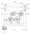
- a defect compensation section 31 in the image-signal-processing device 30 performs any defect compensation on the image signals DRa, DGa, DBa of the three primary colors received from the image pickup device 20 to compensate for a signal level of a pixel signal relative to any defective pixel(s) so that the defective pixel(s) can be inconspicuous.
- the defect compensation section 31 then generates image signals DRb, DGb, DBb and supplies a level adjustment section 32 with these compensated image signals DRb, DGb, DBb.
- the defect-compensation-processing part 31R when a signal relative to the first defective pixel is supplied to the defect-compensation-processing part 31R, the data indicating an amount of offset thereof is supplied to the defect-compensation-processing part 31R as the defect information RPR Alternatively, when a signal relative to the second defective pixel is supplied to the defect-compensation-processing part 31R, the data, which is peculiar to the second defective pixel, indicating the second defective pixel is supplied to the defect-compensation-processing part 31R as the defect information RPR
- the second compensation unit 314 compensates for the pixel signal relative to the first defective pixel(s) without using the compensation signal, so that any over-compensation-free defect compensation can be performed.
- An image signal DRa is supplied to both of the first and second compensation units 312, 314 in the defect-compensation-processing part 131R
- the first compensation unit 312 performs any compensation on the image signal DRa so that a pixel signal relative to the first defective pixel(s) can be compensated.
- the first compensation unit 312 then generates a compensated image signal DRah and supplies a fixed terminal Pa of a signal changeover switch 315 with the compensated image signal DRah.
- the second compensation unit 314 performs any compensation on the image signal DRa so that the pixel signal relative to the second defective pixel(s) can be compensated.
Landscapes
- Engineering & Computer Science (AREA)
- Multimedia (AREA)
- Signal Processing (AREA)
- Transforming Light Signals Into Electric Signals (AREA)
Applications Claiming Priority (1)
| Application Number | Priority Date | Filing Date | Title |
|---|---|---|---|
| JP2006221226A JP2008048104A (ja) | 2006-08-14 | 2006-08-14 | 撮像装置と欠陥補正回路および欠陥補正方法 |
Publications (2)
| Publication Number | Publication Date |
|---|---|
| EP1890478A2 true EP1890478A2 (de) | 2008-02-20 |
| EP1890478A3 EP1890478A3 (de) | 2010-08-18 |
Family
ID=38530942
Family Applications (1)
| Application Number | Title | Priority Date | Filing Date |
|---|---|---|---|
| EP07253162A Withdrawn EP1890478A3 (de) | 2006-08-14 | 2007-08-10 | Bildaufnahmevorrichtung, Fehlerausgleichsvorrichtung und Fehlerausgleichsverfahren |
Country Status (6)
| Country | Link |
|---|---|
| US (1) | US7872679B2 (de) |
| EP (1) | EP1890478A3 (de) |
| JP (1) | JP2008048104A (de) |
| KR (1) | KR101399011B1 (de) |
| CN (1) | CN101127840B (de) |
| TW (1) | TWI346503B (de) |
Families Citing this family (12)
| Publication number | Priority date | Publication date | Assignee | Title |
|---|---|---|---|---|
| JP5563283B2 (ja) * | 2009-12-09 | 2014-07-30 | キヤノン株式会社 | 画像処理装置 |
| JP5616442B2 (ja) * | 2010-06-09 | 2014-10-29 | 富士フイルム株式会社 | 撮像装置及び画像処理方法 |
| EP2613452B1 (de) * | 2010-09-01 | 2022-12-28 | Nec Corporation | Digitale filtervorrichtung, digitales filterverfahren und steuerprogramm für die digitale filtervorrichtung |
| JP5943596B2 (ja) | 2011-12-19 | 2016-07-05 | キヤノン株式会社 | 撮像装置 |
| CN104254871B (zh) * | 2012-04-23 | 2017-10-27 | 英派尔科技开发有限公司 | 扭曲校正可变形显示器 |
| JP6004768B2 (ja) * | 2012-06-14 | 2016-10-12 | キヤノン株式会社 | 焦点検出のための信号処理装置、信号処理方法およびプログラム、ならびに焦点検出装置を有する撮像装置 |
| US8873615B2 (en) * | 2012-09-19 | 2014-10-28 | Avago Technologies General Ip (Singapore) Pte. Ltd. | Method and controller for equalizing a received serial data stream |
| JP6225328B2 (ja) * | 2013-02-18 | 2017-11-08 | パナソニックIpマネジメント株式会社 | 欠陥画素の補正装置および補正方法 |
| JP2015177256A (ja) * | 2014-03-13 | 2015-10-05 | 株式会社東芝 | 固体撮像装置 |
| KR102321110B1 (ko) * | 2015-04-17 | 2021-11-03 | 엘지전자 주식회사 | 촬영 장치 및 촬영 장치의 제어 방법 |
| US9876996B2 (en) * | 2015-12-30 | 2018-01-23 | Gopro, Inc. | Focal compensation for thermal expansion of camera optics using chromatic aberration |
| CN107991310B (zh) * | 2017-11-27 | 2020-11-06 | 上海卫星装备研究所 | 一种应用于航天器表面osr粘贴胶层缺陷检测方法及系统 |
Citations (2)
| Publication number | Priority date | Publication date | Assignee | Title |
|---|---|---|---|---|
| JP2000209506A (ja) | 1999-01-14 | 2000-07-28 | Toshiba Corp | 撮像装置および撮像方法 |
| EP1130907A2 (de) | 2000-03-03 | 2001-09-05 | The Boeing Company | Infrarot-Sensor mit einem Temperatur kompensierten Verlauf und einer Offset-Korrektur |
Family Cites Families (13)
| Publication number | Priority date | Publication date | Assignee | Title |
|---|---|---|---|---|
| US5047863A (en) | 1990-05-24 | 1991-09-10 | Polaroid Corporation | Defect correction apparatus for solid state imaging devices including inoperative pixel detection |
| JP3104098B2 (ja) | 1992-03-18 | 2000-10-30 | ソニー株式会社 | 固体撮像素子の自動欠陥補正回路 |
| JPH06113211A (ja) | 1992-09-28 | 1994-04-22 | Sony Corp | 固体撮像素子の欠陥補正装置 |
| JPH06303531A (ja) | 1993-04-09 | 1994-10-28 | Olympus Optical Co Ltd | 固体撮像素子の画素欠陥補正装置 |
| JP3014895B2 (ja) | 1993-06-02 | 2000-02-28 | 株式会社日立製作所 | ビデオカメラ |
| JPH07236093A (ja) * | 1994-02-21 | 1995-09-05 | Toshiba Medical Eng Co Ltd | 撮像装置 |
| JPH08251484A (ja) | 1995-03-13 | 1996-09-27 | Canon Inc | 撮像装置 |
| GB9825086D0 (en) * | 1998-11-17 | 1999-01-13 | Vision Group Plc | Defect correction in electronic imaging systems |
| JP2002354340A (ja) * | 2001-05-24 | 2002-12-06 | Olympus Optical Co Ltd | 撮像装置 |
| US6985180B2 (en) * | 2001-06-19 | 2006-01-10 | Ess Technology, Inc. | Intelligent blemish control algorithm and apparatus |
| US7092017B2 (en) * | 2002-09-13 | 2006-08-15 | Eastman Kodak Company | Fixed pattern noise removal in CMOS imagers across various operational conditions |
| JP4346968B2 (ja) | 2003-06-13 | 2009-10-21 | キヤノン株式会社 | 放射線撮影方法、放射線撮影装置、及びコンピュータプログラム |
| JP4754939B2 (ja) * | 2005-11-01 | 2011-08-24 | オリンパス株式会社 | 画像処理装置 |
-
2006
- 2006-08-14 JP JP2006221226A patent/JP2008048104A/ja active Pending
-
2007
- 2007-08-07 TW TW096129054A patent/TWI346503B/zh not_active IP Right Cessation
- 2007-08-09 KR KR1020070080263A patent/KR101399011B1/ko not_active Expired - Fee Related
- 2007-08-10 EP EP07253162A patent/EP1890478A3/de not_active Withdrawn
- 2007-08-13 US US11/891,872 patent/US7872679B2/en not_active Expired - Fee Related
- 2007-08-14 CN CN2007101404498A patent/CN101127840B/zh not_active Expired - Fee Related
Patent Citations (2)
| Publication number | Priority date | Publication date | Assignee | Title |
|---|---|---|---|---|
| JP2000209506A (ja) | 1999-01-14 | 2000-07-28 | Toshiba Corp | 撮像装置および撮像方法 |
| EP1130907A2 (de) | 2000-03-03 | 2001-09-05 | The Boeing Company | Infrarot-Sensor mit einem Temperatur kompensierten Verlauf und einer Offset-Korrektur |
Also Published As
| Publication number | Publication date |
|---|---|
| TW200828998A (en) | 2008-07-01 |
| TWI346503B (en) | 2011-08-01 |
| CN101127840B (zh) | 2011-10-26 |
| US20080036883A1 (en) | 2008-02-14 |
| KR20080015365A (ko) | 2008-02-19 |
| KR101399011B1 (ko) | 2014-05-26 |
| EP1890478A3 (de) | 2010-08-18 |
| JP2008048104A (ja) | 2008-02-28 |
| US7872679B2 (en) | 2011-01-18 |
| CN101127840A (zh) | 2008-02-20 |
Similar Documents
| Publication | Publication Date | Title |
|---|---|---|
| US7872679B2 (en) | Image pickup apparatus, defect compensation device, and defect-compensating method | |
| KR100363827B1 (ko) | 넓은 다이내믹레인지의 영상신호를 생성하는텔레비젼신호처리장치와 그 신호처리장치를 가지는텔레비젼카메라 및 텔레비젼신호처리방법 | |
| US6593970B1 (en) | Imaging apparatus with dynamic range expanded, a video camera including the same, and a method of generating a dynamic range expanded video signal | |
| JP3709566B2 (ja) | 映像信号処理装置、カラービデオカメラ及び映像信号の処理方法 | |
| CN102170530B (zh) | 信号处理设备及方法、固态图像捕获设备和电子信息器件 | |
| US20020071041A1 (en) | Enhanced resolution mode using color image capture device | |
| US20110205392A1 (en) | Image capture device | |
| US7830420B2 (en) | Composite image data generating apparatus, method of controlling the same, and program for controlling the same | |
| US8144216B2 (en) | Imaging apparatus and imaging method | |
| JPS62111590A (ja) | 撮像装置 | |
| US6563534B1 (en) | High definition television camera apparatus for correcting a characteristic value of a video signal | |
| US8885062B2 (en) | Auto white balance adjustment system, auto white balance adjustment method, and camera module | |
| US7466352B2 (en) | Gamma correction device in image capturing apparatus | |
| JP2557620B2 (ja) | 撮像装置 | |
| JPH0461558B2 (de) | ||
| JP4145704B2 (ja) | ホワイトバランス回路 | |
| JPH04140992A (ja) | 撮像装置 | |
| JP5597124B2 (ja) | 画像信号処理装置 | |
| KR19980014689A (ko) | 히스토그램을 이용한 감마보정장치 | |
| JPH04142177A (ja) | ビデオカメラ | |
| JP2003037775A (ja) | 撮像装置 | |
| JP2004357238A (ja) | 撮像装置及びその画像処理方法 | |
| JPH0746605A (ja) | 信号処理回路 | |
| JP2007124533A (ja) | 画像撮像装置及び撮像画像処理方法 | |
| JPH02132987A (ja) | 3板式カラーテレビジョンカメラ |
Legal Events
| Date | Code | Title | Description |
|---|---|---|---|
| PUAI | Public reference made under article 153(3) epc to a published international application that has entered the european phase |
Free format text: ORIGINAL CODE: 0009012 |
|
| AK | Designated contracting states |
Kind code of ref document: A2 Designated state(s): AT BE BG CH CY CZ DE DK EE ES FI FR GB GR HU IE IS IT LI LT LU LV MC MT NL PL PT RO SE SI SK TR |
|
| AX | Request for extension of the european patent |
Extension state: AL BA HR MK YU |
|
| PUAL | Search report despatched |
Free format text: ORIGINAL CODE: 0009013 |
|
| AK | Designated contracting states |
Kind code of ref document: A3 Designated state(s): AT BE BG CH CY CZ DE DK EE ES FI FR GB GR HU IE IS IT LI LT LU LV MC MT NL PL PT RO SE SI SK TR |
|
| AX | Request for extension of the european patent |
Extension state: AL BA HR MK RS |
|
| 17P | Request for examination filed |
Effective date: 20110214 |
|
| AKX | Designation fees paid |
Designated state(s): DE FR GB |
|
| STAA | Information on the status of an ep patent application or granted ep patent |
Free format text: STATUS: THE APPLICATION HAS BEEN WITHDRAWN |
|
| 18W | Application withdrawn |
Effective date: 20150108 |