EP1895591A2 - Herstellungsverfahren für eine fotoelektrische Wandlervorrichtung - Google Patents
Herstellungsverfahren für eine fotoelektrische Wandlervorrichtung Download PDFInfo
- Publication number
- EP1895591A2 EP1895591A2 EP07114764A EP07114764A EP1895591A2 EP 1895591 A2 EP1895591 A2 EP 1895591A2 EP 07114764 A EP07114764 A EP 07114764A EP 07114764 A EP07114764 A EP 07114764A EP 1895591 A2 EP1895591 A2 EP 1895591A2
- Authority
- EP
- European Patent Office
- Prior art keywords
- electroconductor
- photoelectric conversion
- mos transistor
- interlayer insulation
- hole
- Prior art date
- Legal status (The legal status is an assumption and is not a legal conclusion. Google has not performed a legal analysis and makes no representation as to the accuracy of the status listed.)
- Granted
Links
Images


Classifications
-
- H—ELECTRICITY
- H10—SEMICONDUCTOR DEVICES; ELECTRIC SOLID-STATE DEVICES NOT OTHERWISE PROVIDED FOR
- H10F—INORGANIC SEMICONDUCTOR DEVICES SENSITIVE TO INFRARED RADIATION, LIGHT, ELECTROMAGNETIC RADIATION OF SHORTER WAVELENGTH OR CORPUSCULAR RADIATION
- H10F39/00—Integrated devices, or assemblies of multiple devices, comprising at least one element covered by group H10F30/00, e.g. radiation detectors comprising photodiode arrays
- H10F39/011—Manufacture or treatment of image sensors covered by group H10F39/12
- H10F39/014—Manufacture or treatment of image sensors covered by group H10F39/12 of CMOS image sensors
-
- H—ELECTRICITY
- H10—SEMICONDUCTOR DEVICES; ELECTRIC SOLID-STATE DEVICES NOT OTHERWISE PROVIDED FOR
- H10F—INORGANIC SEMICONDUCTOR DEVICES SENSITIVE TO INFRARED RADIATION, LIGHT, ELECTROMAGNETIC RADIATION OF SHORTER WAVELENGTH OR CORPUSCULAR RADIATION
- H10F39/00—Integrated devices, or assemblies of multiple devices, comprising at least one element covered by group H10F30/00, e.g. radiation detectors comprising photodiode arrays
- H10F39/80—Constructional details of image sensors
- H10F39/802—Geometry or disposition of elements in pixels, e.g. address-lines or gate electrodes
-
- H—ELECTRICITY
- H10—SEMICONDUCTOR DEVICES; ELECTRIC SOLID-STATE DEVICES NOT OTHERWISE PROVIDED FOR
- H10F—INORGANIC SEMICONDUCTOR DEVICES SENSITIVE TO INFRARED RADIATION, LIGHT, ELECTROMAGNETIC RADIATION OF SHORTER WAVELENGTH OR CORPUSCULAR RADIATION
- H10F39/00—Integrated devices, or assemblies of multiple devices, comprising at least one element covered by group H10F30/00, e.g. radiation detectors comprising photodiode arrays
- H10F39/80—Constructional details of image sensors
- H10F39/803—Pixels having integrated switching, control, storage or amplification elements
- H10F39/8037—Pixels having integrated switching, control, storage or amplification elements the integrated elements comprising a transistor
-
- H—ELECTRICITY
- H10—SEMICONDUCTOR DEVICES; ELECTRIC SOLID-STATE DEVICES NOT OTHERWISE PROVIDED FOR
- H10F—INORGANIC SEMICONDUCTOR DEVICES SENSITIVE TO INFRARED RADIATION, LIGHT, ELECTROMAGNETIC RADIATION OF SHORTER WAVELENGTH OR CORPUSCULAR RADIATION
- H10F39/00—Integrated devices, or assemblies of multiple devices, comprising at least one element covered by group H10F30/00, e.g. radiation detectors comprising photodiode arrays
- H10F39/80—Constructional details of image sensors
- H10F39/811—Interconnections
-
- H—ELECTRICITY
- H10—SEMICONDUCTOR DEVICES; ELECTRIC SOLID-STATE DEVICES NOT OTHERWISE PROVIDED FOR
- H10F—INORGANIC SEMICONDUCTOR DEVICES SENSITIVE TO INFRARED RADIATION, LIGHT, ELECTROMAGNETIC RADIATION OF SHORTER WAVELENGTH OR CORPUSCULAR RADIATION
- H10F39/00—Integrated devices, or assemblies of multiple devices, comprising at least one element covered by group H10F30/00, e.g. radiation detectors comprising photodiode arrays
- H10F39/10—Integrated devices
- H10F39/12—Image sensors
- H10F39/18—Complementary metal-oxide-semiconductor [CMOS] image sensors; Photodiode array image sensors
-
- H—ELECTRICITY
- H10—SEMICONDUCTOR DEVICES; ELECTRIC SOLID-STATE DEVICES NOT OTHERWISE PROVIDED FOR
- H10F—INORGANIC SEMICONDUCTOR DEVICES SENSITIVE TO INFRARED RADIATION, LIGHT, ELECTROMAGNETIC RADIATION OF SHORTER WAVELENGTH OR CORPUSCULAR RADIATION
- H10F39/00—Integrated devices, or assemblies of multiple devices, comprising at least one element covered by group H10F30/00, e.g. radiation detectors comprising photodiode arrays
- H10F39/80—Constructional details of image sensors
- H10F39/803—Pixels having integrated switching, control, storage or amplification elements
-
- H—ELECTRICITY
- H10—SEMICONDUCTOR DEVICES; ELECTRIC SOLID-STATE DEVICES NOT OTHERWISE PROVIDED FOR
- H10W—GENERIC PACKAGES, INTERCONNECTIONS, CONNECTORS OR OTHER CONSTRUCTIONAL DETAILS OF DEVICES COVERED BY CLASS H10
- H10W20/00—Interconnections in chips, wafers or substrates
- H10W20/01—Manufacture or treatment
- H10W20/031—Manufacture or treatment of conductive parts of the interconnections
- H10W20/056—Manufacture or treatment of conductive parts of the interconnections by filling conductive material into holes, grooves or trenches
Definitions
- the present invention relates to a manufacturing method of a photoelectric conversion device.
- the photoelectric conversion device used in digital cameras and video cameras includes a CCD type and a MOS type photoelectric conversion device.
- a MOS type photoelectric conversion device includes a photoelectric conversion region including a MOS transistor and a photodiode and a peripheral circuit region including a MOS transistor outputting signals of the photoelectric conversion region and driving the MOS transistor arranged in the photoelectric conversion region.
- Those photoelectric conversion region and peripheral circuit region can be manufactured through a common step by a CMOS manufacturing process.
- Japanese Patent Application Laid-Open No. H09-055440 describes contact structure used at an occasion of manufacturing an SRAM by the CMOS manufacturing process. Specifically, in structure, a semiconductor region is electrically connected to a gate electrode with an electroconductor buried in a hole arranged in an interlayer insulation layer and a plurality of layers of an electroconductor arranged in a hole arranged in an interlayer insulation layer are stacked.
- Japanese Patent Application Laid-Open No. 2002-368203 discloses, in a source follower circuit present in a peripheral circuit region of a CCD type photoelectric conversion device, a constitution of electrically connecting a semiconductor region to a gate electrode with an electroconductor buried in a hole arranged in an interlayer insulation layer.
- a MOS photoelectric conversion device requires more wiring layers in number than a CCD photoelectric conversion device since one pixel includes a photoelectric conversion element and a plurality of MOS transistors.
- a light incident aperture of the photoelectric conversion element is defined by the wiring layer. Accordingly, in order to increase optical incidence efficiency to improve sensitivity, a wiring layout for widening the aperture for optical incidence to the photoelectric conversion element will be required.
- present inventor has found out to adopt a constitution to electrically connect a semiconductor region to a gate electrode with an electroconductor buried in a hole arranged in an interlayer insulation layer. And, at some occasion of manufacturing a photoelectric conversion device in such a constitution, noises were found to occasionally increase.
- an object of the present invention is to restrain noise increase being the above described newly found problem and to provide a manufacturing method of a MOS photoelectric conversion device which has been improved in efficiency of optical incidence to a photoelectric conversion element.
- a manufacturing method of a photoelectric conversion device of the present invention is a manufacturing method of a photoelectric conversion device including: a plurality of photoelectric conversion elements arranged on a semiconductor substrate: and a transfer MOS transistor for transferring an electric carrier of the photoelectric conversion element to a first semiconductor region, and an amplifying MOS transistor for reading out a signal based on the electric carrier transferred, including steps of: forming the photoelectric conversion element, the first semiconductor region, the transfer MOS transistor and the amplifying MOS transistor on a semiconductor substrate; forming a first interlayer insulation layer covering the photoelectric conversion element, the transfer MOS transistor and the amplifying MOS transistor; forming a single hole in the first interlayer insulation layer to expose a region including a part of a gate electrode of the amplifying MOS transistor and a part of the first semiconductor region; forming a hole in the first interlayer insulation layer to expose a region including a part of an electrode of the amplifying MOS transistor and a part of the first semiconductor region; burying in the single hole
- a manufacturing method of a photoelectric conversion device of the present invention is a manufacturing method of a photoelectric conversion device including: and a photoelectric conversion element, and a plurality of MOS transistors including a transfer MOS transistor for transferring a electric carrier of the photoelectric conversion element to a first semiconductor region and an amplifying MOS transistor for reading out a signal based on the electric carrier transferred, being arranged in a semiconductor substrate; and a wiring layer including a plurality of wirings, a plurality of interlayer insulation layers including a first interlayer insulation layer arranged to cover the photoelectric conversion element and the plurality of MOS transistors, and a second interlayer insulation layer laminated on the first interlayer insulation layer, being arranged on a semiconductor substrate, wherein the photoelectric conversion device further includes first and second electroconductors, the first electroconductor is buried in a first hole arranged in the first interlayer insulation layer, the second electroconductor for electrically connecting the first semiconductor region to a gate electrode of the amplifying MOS transistor not through the
- FIG. 1 is a schematic section of a photoelectric conversion device of a first embodiment.
- FIGS. 2A, 2B, 2C and 2D are schematic views illustrating manufacturing steps of a photoelectric conversion device.
- FIG. 3 is a schematic section of a photoelectric conversion device of a second embodiment.
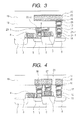
- FIG. 4 is a schematic section of a photoelectric conversion device for comparison.
- FIG. 5A is a plan layout view of a photoelectric conversion device and FIG. 5B is a plan layout view of photoelectric conversion device for comparison.
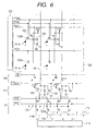
- FIG. 6 is an example of a circuit of a photoelectric conversion device.
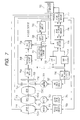
- FIG. 7 is a block diagram of an example of an image pickup system.
- FIGS. 8A and 8B are plan layout views of a MOS transistor.
- FIG. 9 is a plan layout view on a first electroconductor.
- FIG. 10 is a graph on contact resistance.
- FIG. 11 is a schematic section of a photoelectric conversion device of a fourth embodiment.
- a photoelectric conversion device of the present invention includes a plurality of photoelectric conversion elements arranged on a semiconductor substrate, a plurality of MOS transistors and wiring arranged on the semiconductor substrate.
- Those MOS transistors include at least transfer MOS transistor which transfers electric carriers of the photoelectric conversion element to a first semiconductor region and an amplifying MOS transistor which reads signals based on transferred electric carriers.
- the photoelectric conversion device includes a first interlayer insulation layer arranged on a semiconductor substrate covering the photoelectric conversion element and a plurality of the MOS transistors and a second interlayer insulation layer stacked on the first interlayer insulation layer.
- the first electroconductor buried in the first hole arranged on the first interlayer insulation layer is used to electrically connect the first semiconductor region to the gate electrode of the amplifying MOS transistor through no wiring.
- a second semiconductor region different from the first semiconductor region is electrically connected to wiring by the second electroconductor.
- the second electroconductor is structured by stacking and electrically connecting a third electroconductor buried in a second hole arranged in the first interlayer insulation layer and a fourth electroconductor buried in a third hole arranged in the second interlayer insulation layer. And that third electroconductor is buried in each hole through the same step as the step for the first electroconductor.
- Such constitution will enable electrical connection between the first semiconductor region and the gate electrode without wiring and therefore decreases in the quantity of required wiring and improves the degree of freedom in designing wiring and can improve the aperture ratio of a photoelectric conversion element.
- the first electroconductor and the third electroconductor are formed through the same step. Thereby diffusion of metal impurity to the semiconductor region decreases to enable simplification of the manufacturing step. Accordingly, while decreasing in increase in noise, it will be enabled to widen the aperture of a photoelectric conversion device to enable provision of a photoelectric conversion device with improved signal-to-noise ratio.
- first electroconductor and the third electroconductor have the same height so that planarization of an interlayer insulation layer arranged on the first electroconductor and the third electroconductor will become easy.
- an interlayer insulation layer can be thinned. Therefore the incident light path to a photoelectric conversion element can be shortened. And light entering the photoelectric conversion element can be increased more.
- metal impurity diffuses in an active region (semiconductor region) to increase dark current to generate a noise and give rise to variation in signals of each pixel.
- active region semiconductor region
- properties of the photoelectric conversion element will remarkably decrease. Noises due to metal impurity will significantly influence image qualities. Therefore there will be, in particular, problem in the photoelectric conversion device.
- the first electroconductor is formed on a first interlayer insulation layer and thereafter a hole for electrical connection portion in another region is formed in the first interlayer insulation layer.
- a semiconductor substrate is exposed in a metal atmosphere after forming the first electroconductor, metal occasionally diffuses in the substrate.
- an electroconductor bringing respective regions into electrical connection There exist two kinds of electroconductor arranged in a hole arranged in an interlayer insulation layer according to an object brought into electrical connection.
- One is a contact plug to electrically connect an active region to an electroconductor such as wiring or a gate electrode to an electroconductor such as wiring.
- the other one is a via plug to electrically connect a contact plug to wiring or wirings themselves.
- shared contact construction structure of bringing different regions and members into electrical connection only with a plug not through wirings.
- stacked contact structure structure including the above described first electroconductor can be called shared contact structure.
- Structure including the second electroconductor can be called as stacked (stacked via) contact.
- barrier film can be arranged between a hole and an electroconductor. The barrier film is provided in an attempt to restrain alloy reaction between the interlayer insulation layer, the substrate and the like and the electroconductor or restrain diffusion of the electroconductor to the interlayer insulation layer, the substrate and the like. In a likewise attempt, barrier film can be provided to the upper portion and the lower portion of the wiring as well.
- An aperture refers to a region where light is allowed to enter a photoelectric conversion element and is generally defined by a pattern of wiring and light shielding film.
- the pattern stipulating the aperture is to determine an outer circumference of light entering the photoelectric conversion element, and optical simulation and the like of the section of the photoelectric conversion device will bring into knowledge which pattern determines the aperture.
- a semiconductor substrate being a material substrate will be referred to as "substrate” and includes a case where a material substrate as described below undergoes treatment.
- substrate a member in the state where one or a plurality of semiconductor regions and the like are formed, or a member midway a series of manufacturing steps or a member subjected to a series of manufacturing steps can be referred to as substrate as well.
- An active region refers to a semiconductor region partitioned by an element isolation region formed by a LOCOS and the like or a region where a various elements are formed or configuring a part of an element.
- a drain region and a source region in a transistor are included.
- FIG. 6 exemplifies a circuit of a MOS photoelectric conversion device.
- Transfer MOS transistors 102a and 102b transfer electric carriers of the photoelectric conversion elements.
- electrons among electric carriers generated in a photoelectric conversion element are treated as signal electric carriers.
- the transfer MOS transistor is an N type.
- a reset MOS transistor 103 resets the photoelectric conversion elements 101a and 101b and the drain region of the transfer MOS transistor.
- an amplifying MOS transistor 104 amplifies signals based on electric carrier generated in the photoelectric conversion element and outputs the signals to a signal line 106.
- the amplifying MOS transistor is adapted as a part of a source follower circuit and the drain region thereof is supplied with power source voltage.
- a selection MOS transistor 105 controls reading to a signal line.
- the transfer transistor, the reset transistor, the amplifying MOS transistor and a selection MOS transistor will be inclusively referred to as reading MOS transistors.
- the reset MOS transistor 103, the amplifying MOS transistor 104 and the selection MOS transistor 105 included in that reading MOS transistor are shared with the two photoelectric conversion elements 101a and 101b.
- the photoelectric conversion element is arranged in the photoelectric conversion region 124.
- a clump circuit 108, a cascade amplifier portion 120 and a signal retaining portion 121 adapted to include clump capacity are provided on each signal line 106.
- the signal retaining portion 121 is adapted to include capacitors 112a and 112b, a switch and the like.
- Scan circuits 123 and 129 are included. Signals generated in the photoelectric conversion elements 101a and 101b are read from the signal output line 106 by a read transistor driven by the scan circuit 123 and are output to horizontal output lines 116a and 116b through the clump circuit 108 and the signal retaining portion 121. The signals of the horizontal output lines 116a and 116b are finally output from a differential amplifier 118.
- Noise components are removed from signals in the clump circuit 108 and the differential amplifier 118 to become image signals.
- the portions such as the scan circuit and the clump circuit besides the photoelectric conversion region 124 are collectively referred to as a periphery circuit region.
- shared contact structure is employed for a first electroconductor bringing the semiconductor region (first semiconductor region) where electric carrier generated in the photoelectric conversion element are transferred and the gate electrode of the amplifying MOS transistor into electrical connection.
- stacked contact structure is employed for electrically connecting the other MOS transistors and the wiring.
- FIG. 1 is a schematic section of a pixel of a photoelectric conversion device of a first embodiment.
- FIG. 1 corresponds to the portion including the photoelectric conversion element 101 and the transfer MOS transistor 102 in FIG. 6.
- a semiconductor region 1 of a first electroconductor type is provided on one main plane of the substrate. That semiconductor region 1 can be one of a well and a substrate of the first electroconductor type.
- a photoelectric conversion element includes a semiconductor region 2 of a second electroconductor type.
- a semiconductor region 3 of the first electroconductor type covers the semiconductor region 2.
- a gate electrode 4 of the transfer MOS transistor transfers electric carriers of the photoelectric conversion element.
- the electric carriers of the photoelectric conversion element are transferred to a semiconductor region 5 (hereinafter to be referred to as a floating diffusion region, that is, FD region) of the second electroconductor type.
- An element isolation region 6 is an STI (Shallow Trench Isolation) structure in the present embodiment.
- the source follower circuit includes a gate electrode 7 of the amplifying MOS transistor.
- An active region (semiconductor region) 8 in the pixel is connected to the wiring.
- the active region connected to the wiring is an electrode region, for example, selected from the group including of the source region, the drain region and the like of the above described read MOS transistor. Otherwise, there is a well contact for supplying the well with voltage.
- the gate electrode includes the case of being integrated with wirings connecting FD regions to each other and wirings supplying the gate electrode with voltage.
- a first electroconductor 9 electrically connects the FD region 5 to the gate electrode 7 of the amplifying MOS transistor.
- the first electroconductor is arranged in a single contact hole (first hole) arranged in the first interlayer insulation layer 17. The first electroconductor brings the gate electrode 7 and the FD region 5 into electrical connection not through wirings.
- the second electroconductors 11 and 13 electrically connect the active region 8 to the wiring 15.
- the second electroconductor includes a third electroconductor and a fourth electroconductor stacked and brought into electrical connection. That third electroconductor 11 is arranged in a second hole arranged in the first interlayer insulation layer 17.
- the fourth electroconductor 13 is arranged in a third hole arranged in the second interlayer insulation layer 18.
- Barrier film 10, 12 and 14 is arranged between an electroconductor and an interlayer insulation layer.
- barrier film 16 is arranged in the upper and the lower portions of the wiring 15. Interlayer insulation layers 17, 18 and 19 insulate the wiring, contact and the like.
- the gate electrode 7 coming into electrical connection with the first electroconductor is arranged over the element isolation region 6.
- That element isolation region 6 is desirably STI structure.
- the element isolation region is LOCOS structure
- etching at an occasion of forming a hole where the first electroconductor is arranged damages a bird's beak portion of the LOCOS structure to increase a leakage current.
- the LOCOS structure is higher than the STI structure in height from a substrate and, therefore, process control at the time of forming a hole is difficult.
- the element isolation region can be STI structure.
- the gate electrode 7 arranged over the element isolation region 6 can function as wiring.
- FIG. 4 For the purpose of comparison, structure in which the gate of the amplifying MOS transistor and the FD region are brought into electrical connection through two electroconductors and wiring will be described with FIG. 4.
- an electroconductor 26 an electroconductor 27 and a wiring 28. That is, unlike the structure in FIG. 1, an additional wiring 28 will be required in the same layer (height) as the wiring 15.
- the wiring layer decreases in the degree of freedom of layout to occasionally narrow an aperture of the photoelectric conversion element.
- no wiring is required at an occasion of electrically connecting the gate electrode 7 to the FD region 5. Therefore, the wiring layer increases in the degree of freedom of layout.
- the aperture of the photoelectric conversion element can be widened.
- the wiring can be arranged in a desired region in a part of a region immediately above the first electroconductor over the second interlayer insulation layer. Thereby, shielding of the FD region 5 will become easy.
- FIG. 5A illustrates a plan layout view of a photoelectric conversion device with a first electroconductor (shared contact structure) electrically connected to the gate electrode of an amplifying MOS transistor.
- FIG. 5A corresponds to FIG. 6 in reference numeral and description thereon will be omitted.
- An FD region is electrically connected to the gate electrode of the amplifying MOS transistor 104 with the first electroconductor 9.
- an active region 130 is electrically connected to a power source.
- FIG. 5B illustrates a plan layout view of a photoelectric conversion device without any first electroconductor for bringing the gate electrode of the amplifying MOS transistor into electrical connection as in the constitution as in FIG. 4, for example.
- FIG. 6 likewise corresponds to FIG. 5A in reference numeral.
- FIG. 5B illustrates wiring 133 for bringing the signal output line 106, the power source line 107, the FD region and the gate electrode into electrical connection and there are more wiring in number per a pixel than in FIG. 5A. Consequently, by adapting the structure of the present embodiment, the wiring layer increases the degree of freedom in layout so that the aperture of the photoelectric conversion element can be widened. In addition, the wiring is arranged over the FD region.
- the wiring is not a drive line electrically connected to the gate electrode of the MOS transistor but one of the signal output line 106 and the power source line 107, the noise to the FD region due to variation in potential of the wiring can be decreased further.
- the active region 8 inside a pixel is provided with the second an electroconductor for bringing the wiring in the upper portion into electrical connection.
- That second electroconductor can also be formed of one electroconductor.
- a hole is formed to pierce the first interlayer insulation layer and the second interlayer insulation layer to bury an electroconductor there.
- metal impurity can possibly diffuse into the active region 8. Therefore, in structure of the present embodiment, the third electroconductor 11 and the first electroconductor 9 on the substrate side are formed through the same step. Thereafter fourth electroconductor 13 is stacked over the third electroconductor. Thereby, entrance of metal impurity into the semiconductor region decreases and a photoelectric conversion device with less noise can be provided.
- the third electroconductor and the first electroconductor approximately have the same height.
- planarization of the second interlayer insulation layer arranged over those electroconductors can be simplified to enable the interlayer insulation layer to get thinner.
- incident light path to the photoelectric conversion element can be shortened.
- FIGS. 2A, 2B, 2C and 2D correspond to FIG. 1 in reference numeral.
- an element isolation region 6, a second electroconductor type semiconductor region 3, FD region 5 and the like are formed in a semiconductor region 1 of a first electroconductor type.
- gate electrodes 4 and 7 made of polysilicon, for example are formed on a semiconductor substrate to provide the sate where a photoelectric conversion element and a MOS transistor are formed in a semiconductor substrate.
- a first interlayer insulation layer 17 made of silicon oxide film is formed to provide a constitution of FIG. 2A.
- the hole 21 is a single hole corresponding to a region including a part of the gate electrode of an amplifying MOS transistor and a part of the FD region.
- the hole 22 is formed in a region corresponding to at least a part of one of the source and the drain regions being electrode regions of the read transistor.
- the shape of the hole can be for covering all the region of each electrode region. The shape can correspond to only the region of a part thereof.
- the read transistor is, for example, an amplifying MOS transistor.
- barrier film 10 and 11 After removing the resist pattern 20, film for forming barrier film 10 and 11 is formed. Moreover, metal film (tungsten film) for forming the first electroconductor 9 and the third electroconductor 11 is formed. Tungsten film is formed by, for example, a CVD method with WF 6 gas. Barrier film in the case where the electroconductor is tungsten includes Ti and TiN, for example. The barrier film can be one of a mono layer and a stacked layer. By etching back the barrier film and the metal film concurrently, the first electroconductor 9 and the third electroconductor 11 including barrier film 10 and 11 are formed. For that step, besides etching back, a CMP (Chemical Mechanical Polishing) method can be adopted.
- CMP Chemical Mechanical Polishing
- Such a step will enable the first electroconductor and the third electroconductor to have the same height.
- the second interlayer insulation layer 18 is formed to give rise to a constitution of FIG. 2C.
- a resist pattern is formed again so that a hole for a fourth electroconductor is formed with the resist pattern as a mask. That hole is formed in a region corresponding to at least a part of the second electroconductor.
- the fourth electroconductor 13 and barrier film 14 are formed (FIG. 2D).
- barrier film, metal film for wiring and barrier film undergoes film forming and patterning in this order. Thereby, wiring 15 and barrier film 16 thereof are formed.
- the fourth electroconductor 13 is electrically connected to the wiring 15.
- the third interlayer insulation layer 19 is formed to give rise to the constitution of FIG. 1. Aluminum is adopted for the metal film of the wiring layer but copper can be adopted.
- FIG. 8A is a schematic plan view for describing the shape of the bottom plane of an electroconductor and includes a gate electrode 30 and an active region 31.
- a shape 29 of the bottom plane of a hole is arranged in the active region 31 and the gate electrode 30.
- the contact is approximately rectangular with a line having length X1 and the other line perpendicular thereto having length Y1. Otherwise there is a case of an oval shape.
- the length X1 is equivalent to the length Y1.
- FIG. 8B is a schematic plan view illustrating the bottom plane 32 of a hole in structure (shared contact structure) including the first electroconductor of FIG. 1.
- FIG. 8B corresponds to FIG. 8A in reference numeral.
- the bottom plane 32 of the hole is also approximately rectangular.
- an oval shape can be adopted.
- the other line has length X2.
- the length Y2 is longer than the length X2.
- the length X2 can be longer than the length X1.
- a first electroconductor 9 arranged in an aperture arranged in the first interlayer insulation layer 17, and a third electroconductor are formed concurrently. Thereby diffusion of metal impurity to the substrate can be reduced. Thereby, a high quality photoelectric conversion device with less noise can be provided.
- the second electroconductor electrically connects the active region 8 to the wiring layer.
- structure of that second electroconductor is also applicable to electrical connection between a gate electrode of a MOS transistor different from an amplifying MOS transistor and the wiring layer.
- FIG. 3 corresponds to FIG. 1 in reference numeral.
- the present embodiment features structure of barrier film included in the second electroconductor. Barrier films 24-1 and 24-2 are provided between the third electroconductor 11 and the active region 8. Barrier film 25 is provided between the fourth electroconductor 13 and the third electroconductor.
- the structure can be formed by providing a step for forming dual layered barrier film in a hole prior to a step for arranging the first electroconductor and the third electroconductor and adding a step for forming a mono layered barrier film in a hole prior to a step for arranging the fourth electroconductor.
- barrier film of the first electroconductor 9 and the third electroconductor 11 is dual layered structure of Ti film and TiN film and barrier film of the fourth electroconductor 13 is a mono layered TiN film. That constitution enables improvement in yield factor of a photoelectric conversion device including structure as the second electroconductor.
- barrier film of the third electroconductor 11 in the lower layer is dual layered structure of Ti film 24-1 being adhesive to Si and TiN film 24-2 being resistant to WF 6 .
- the fourth electroconductor 13 in the upper layer includes only TiN resistant to WF 6 .
- thick TiN film can be arranged and therefore coating ratio can be improved to enable reduction in abnormal growth of tungsten and erosion of barrier film.
- the barrier film in the upper layer can be a mono layered structure of TiN film excellently resistant to WF 6 .
- Such constitution can make TiN thicker than the case where a plurality of layers is provided and enables erosion of barrier film and occurrence of abnormal growth of tungsten to be reduced. Accordingly, the yield factor of a photoelectric conversion device including the contact of the stacked structure can be improved.
- material lower than WF 6 in reactivity is selected from the group including of TaN, WSi, WN and the like.
- the present embodiment stipulates a ratio of a length of a region arranged at a part of the area just above the gate electrode of the amplifying MOS transistor of the first electroconductor (shared contact structure) and a length of a region arranged at a part of the area just above an active region of the first electroconductor. That length stipulation will be described with FIG. 9 and FIG. 10.
- FIG. 9 is a plan view illustrating the bottom plane of the first electroconductor subjected to enlargement in a portion where the first electroconductor 9 is formed in FIG. 5A.
- FIG. 9 corresponds to FIG. 1 in reference numeral.
- FIG. 9 illustrates wirings 301 and 303. Those wirings correspond to the signal line 106 and the power source line 107.
- the first electroconductor 9 includes a first region arranged at a part of the area just above the gate electrode of the amplifying MOS transistor and a second region arranged at a part of the area just above an FD region 5.
- the lengths of the first and the second regions parallel in a direction crossing a boundary between those first and second regions are Z1 and Z2 respectively.
- the lengths Z1 and Z2 are length in the longitudinal direction in a planar shape of the first electroconductor.
- the first electroconductor is substantially shaped rectangular with longer lines in a direction crossing a boundary between the gate electrode 7 and the FD region 5. Shorter lines of the first electroconductor are substantially parallel to a boundary between the gate electrode 7 and the FD region 5. With such a relation, also in a site where arrangement of line and space in the design rule, a sufficient contact area can be secured for the gate electrode 7 and the FD region 5.
- the first electroconductor in view from the top can be shaped oval and the like.
- FIG. 10 is a graph illustrating the relation between contact resistance and the ratio of the lengths of the first and second regions of the first electroconductor illustrated in FIG. 9.
- the ratio Z2/Z1 is the ratio of the lengths of the first and second regions of the first electroconductor, that is, in other words, a percentage of the area of the second region to the area of the first region.
- the ratio Z2/Z1 in FIG. 10 illustrates changes in the length Z2 with Z1 being a constant value. Specifically, changes in contact resistance are illustrated in the case where the length Z1 is fixed at 0.28 and the value of the length Z2 is changed. As illustrated in FIG. 10, with the ratio Z2/Z1 being 0.6 and more, it is apparent that the contact resistance decreases linearly as the ratio Z2/Z1 increases. That is, as the contact areas of the first electroconductor and the gate electrode 7 gets larger than the contact area of the first electroconductor to the FD region 5, the contact resistance decreases linearly.
- the contact resistance increases sharply as the ratio Z2/Z1 decreases. That is, as the contact areas of the first electroconductor and the gate electrode 7 gets smaller than the contact area of the first electroconductor to the FD region 5, the contact resistance increases sharply.
- a photoelectric conversion device forms an image with information of the two-dimensionally arranged pixel. Accordingly the properties of each pixel are desired to be uniform. However, variation and the like at manufacturing occasionally gives rise to variation in size of the bottom plane of the first electroconductor in each pixel. That is, in the case of the ratio Z2/Z1 being less than 0.6, a little variation at manufacturing even gives rise to significant variation in contact resistance. Even if a uniform light amount is irradiated over the whole pixels, in the case where there is significant variation in contact resistance of the first electroconductor, voltage applied to the gate electrode of the amplifying MOS transistor will give rise to variation. Therefore, variation in the output of each pixel occurs to occasionally coarsen an image to be obtained. In contrast, with the ratio Z2/Z1 being 0.6 and more, even if likewise variation occurs at manufacturing, variation in contact resistance is small and therefore variation in output of each pixel can be decreased.
- the ratio Z2/Z1 is desired to be 0.6-1.
- the ratio Z2/Z1 is desired to be 0.7 or more. Thereby contact resistance is stabilized and the control of the process becomes easy.
- structure of the first electroconductor illustrated in the present embodiment enables miniaturization without decreasing electrical properties.
- FIG. 11 is further provided with a reflection preventing film 1101 in addition to the constitution in FIG. 1.
- a wiring 1102 is arranged over the third electroconductor 11 and a wiring 1103 is arranged on the same layer.
- the reflection preventing film 1101 can be used as etching stop film at forming a hole so that a hole can be formed in a well-controlled manner.
- the gate electrode 7 includes a side wall 1104 including the reflection preventing film 1101. At that occasion, in size of the bottom plane of the first electroconductor, the length of the region coming into connection to the side wall 1104 can be included in the above described length Z1.
- FIG. 7 is a block diagram in the case of applying a photoelectric conversion device described with the above described embodiment to a video camera being an example of an image pickup system.
- Another image pickup system is a digital still camera and the like. Details will be described below based on FIG. 7.
- An image pickup lens 701 includes a focus lens 701A for adjusting focus, a zoom lens 701B for zooming and a lens 701c for providing an image.
- the optical system includes an image pickup lens 701 and a diaphragm and a shutter 702.
- a sampling and holding circuit (S/H circuit) 704 samples and holds output signals from the photoelectric conversion device 703 and moreover amplifies the level thereof to output video signals.
- Video signals output from the sampling and holding circuit 704 undergo a predetermined treatment selected from the group including of gamma correction, color separation, blanking treatment and the like with a process circuit 705, which outputs a luminance signal Y and a chroma signal C.
- a chroma signal C output from the process circuit 705 undergoes correction in white balance and color balance with a color signal correction circuit 721 and is output as chrominance difference signals R-Y and B-Y.
- the luminance signal Y output from the process circuit 705 and chrominance difference signals R-Y and B-Y output from the color signal correction circuit 721 are modulated in an encoder circuit (ENC circuit) 724 and output as standard television signal and is supplied to an electronic view finder such as one of a video recorder not illustrated in the drawing and a monitor electronic view finder (EVF). That process circuit 705 and the like are regarded as a signal processing circuit.
- an iris control circuit 706 controls an iris drive circuit 707 based on video signals supplied from the sample hold circuit 704.
- the iris control 706 automatically controls an ig meter 708 to control the aperture amount of a diaphragm 702 so that the level of the video signal gets to a constant value of a predetermined level.
- Band-pass filters (BPF) 713 and 714 extract a high frequency component necessary for carrying out focus detection from the video signal output from the sampling and holding circuit 704. Signals output from the first band-pass filter 713 (BPF 1) and the second band-pass filter 714 (BPF 2) provided with respectively different band limits are held by a focus gate frame in the gate circuit 715. And a peak value is detected and held by the peak detection circuit 716 and simultaneously input to a logic control circuit 717. That signal will be called focus voltage. The focus is adjusted with that focus voltage.
- a focus encoder 718 detects a moving location of a focus lens 701A.
- a zoom encoder 719 detects a focus of a zoom lens 701B.
- An iris encoder 720 detects an aperture amount of the diaphragm 702. The detected values of those encoders are supplied to the logic control circuit 717 which carries out system control.
- the logic control circuit 717 carries out focus detection on a subject to adjust focus based on the video signal corresponding to inside a set focus detection region. That is, peak value information of high frequency component supplied from the respective band-pass filters 713 and 714 is taken in. Thereafter, the focus lens 701A is driven to a position where the peak value of the high frequency component is maximized. Therefore, the focus drive circuit 709 is provided with a control signal selected from the group including of a rotation direction, a rotation velocity, one of rotation and halting and the like of the focus motor 710 to control that focus motor 710.
- the zoom drive circuit 711 rotates the zoom motor 712 when zooming is instructed.
- the zoom lens 701B moves to carry out zooming.
- photoelectric conversion device of the present invention which increases incident light amount to a photoelectric conversion element and has less noise in such an image pickup system can provide an image pickup system with good signal-to-noise ratio.
- the present invention can provide a more high quality photoelectric conversion device and a more high quality image pickup system.
- the material and the manufacturing method selected from the group including of electroconductive type of a semiconductor substrate, a constitution of a pixel, a wiring layout and, otherwise, a stacking number of the second electroconductor and the like will not be limited to the respective embodiments but will be appropriately set.
- first electroconductor arranged in a first hole arranged in the first interlayer insulation layer electrically connects a first semiconductor region to a gate electrode of an amplifying MOS transistor not through wirings included in a wiring layer.
- a second electroconductor electrically connects a second semiconductor region different from the first semiconductor region to a wiring.
- a third electroconductor arranged in a second hole arranged in the first interlayer insulation layer and a fourth electroconductor arranged in a third hole arranged in the second interlayer insulation layer are stacked and electrically connected to each other. And the step of forming the first electroconductor, and the step of forming the third electroconductor are performed simultaneously.
Landscapes
- Solid State Image Pick-Up Elements (AREA)
- Transforming Light Signals Into Electric Signals (AREA)
- Light Receiving Elements (AREA)
Applications Claiming Priority (3)
| Application Number | Priority Date | Filing Date | Title |
|---|---|---|---|
| JP2006235936 | 2006-08-31 | ||
| JP2006236760 | 2006-08-31 | ||
| JP2007189447A JP5305622B2 (ja) | 2006-08-31 | 2007-07-20 | 光電変換装置の製造方法 |
Publications (3)
| Publication Number | Publication Date |
|---|---|
| EP1895591A2 true EP1895591A2 (de) | 2008-03-05 |
| EP1895591A3 EP1895591A3 (de) | 2011-11-30 |
| EP1895591B1 EP1895591B1 (de) | 2013-01-09 |
Family
ID=38669190
Family Applications (1)
| Application Number | Title | Priority Date | Filing Date |
|---|---|---|---|
| EP07114764A Not-in-force EP1895591B1 (de) | 2006-08-31 | 2007-08-22 | Herstellungsverfahren für eine fotoelektrische Wandlervorrichtung |
Country Status (3)
| Country | Link |
|---|---|
| US (2) | US7749788B2 (de) |
| EP (1) | EP1895591B1 (de) |
| JP (1) | JP5305622B2 (de) |
Cited By (1)
| Publication number | Priority date | Publication date | Assignee | Title |
|---|---|---|---|---|
| US11569279B2 (en) | 2017-10-27 | 2023-01-31 | Sony Semiconductor Solutions Corporation | Solid-state imaging device, method of manufacturing solid-state imaging device, and electronic apparatus |
Families Citing this family (30)
| Publication number | Priority date | Publication date | Assignee | Title |
|---|---|---|---|---|
| JP4425809B2 (ja) * | 2005-02-03 | 2010-03-03 | 富士通マイクロエレクトロニクス株式会社 | 撮像装置 |
| JP5110820B2 (ja) | 2006-08-02 | 2012-12-26 | キヤノン株式会社 | 光電変換装置、光電変換装置の製造方法及び撮像システム |
| JP5110831B2 (ja) * | 2006-08-31 | 2012-12-26 | キヤノン株式会社 | 光電変換装置及び撮像システム |
| JP2008181965A (ja) * | 2007-01-23 | 2008-08-07 | Sharp Corp | 積層型光電変換装置及びその製造方法 |
| JP4110192B1 (ja) * | 2007-02-23 | 2008-07-02 | キヤノン株式会社 | 光電変換装置及び光電変換装置を用いた撮像システム |
| JP5159120B2 (ja) * | 2007-02-23 | 2013-03-06 | キヤノン株式会社 | 光電変換装置およびその製造方法 |
| JP5305623B2 (ja) * | 2007-07-20 | 2013-10-02 | キヤノン株式会社 | 光電変換装置及び光電変換装置を用いた撮像システム |
| JP5274166B2 (ja) * | 2008-09-10 | 2013-08-28 | キヤノン株式会社 | 光電変換装置及び撮像システム |
| KR20100045094A (ko) * | 2008-10-23 | 2010-05-03 | 주식회사 동부하이텍 | 이미지 센서의 제조 방법 |
| JP2010161236A (ja) | 2009-01-08 | 2010-07-22 | Canon Inc | 光電変換装置の製造方法 |
| JP2010206173A (ja) | 2009-02-06 | 2010-09-16 | Canon Inc | 光電変換装置およびカメラ |
| JP2010206174A (ja) | 2009-02-06 | 2010-09-16 | Canon Inc | 光電変換装置およびその製造方法ならびにカメラ |
| JP2010206172A (ja) | 2009-02-06 | 2010-09-16 | Canon Inc | 撮像装置およびカメラ |
| JP5451098B2 (ja) * | 2009-02-06 | 2014-03-26 | キヤノン株式会社 | 半導体装置の製造方法 |
| JP5558857B2 (ja) * | 2009-03-09 | 2014-07-23 | キヤノン株式会社 | 光電変換装置およびそれを用いた撮像システム |
| JP5627202B2 (ja) * | 2009-06-18 | 2014-11-19 | キヤノン株式会社 | 固体撮像装置及びその製造方法 |
| JP5558916B2 (ja) * | 2009-06-26 | 2014-07-23 | キヤノン株式会社 | 光電変換装置の製造方法 |
| JP5563257B2 (ja) * | 2009-08-28 | 2014-07-30 | キヤノン株式会社 | 光電変換装置、撮像システム、及び光電変換装置の製造方法 |
| JP2011216865A (ja) * | 2010-03-17 | 2011-10-27 | Canon Inc | 固体撮像装置 |
| US9171799B2 (en) | 2010-03-25 | 2015-10-27 | Canon Kabushiki Kaisha | Photoelectric conversion apparatus, image pickup system, and manufacturing method therefor |
| JP6188281B2 (ja) * | 2012-05-24 | 2017-08-30 | キヤノン株式会社 | 光電変換装置 |
| JP6041607B2 (ja) | 2012-09-28 | 2016-12-14 | キヤノン株式会社 | 半導体装置の製造方法 |
| JP6128787B2 (ja) * | 2012-09-28 | 2017-05-17 | キヤノン株式会社 | 半導体装置 |
| CN106416230B (zh) * | 2014-01-22 | 2019-09-10 | 松下知识产权经营株式会社 | 固体摄像装置以及摄像装置 |
| US9935139B2 (en) | 2014-08-22 | 2018-04-03 | Taiwan Semiconductor Manufacturing Co., Ltd. | Image sensor and method for forming the same |
| JP6700655B2 (ja) | 2014-10-30 | 2020-05-27 | キヤノン株式会社 | 光電変換装置および光電変換装置の製造方法 |
| KR101676810B1 (ko) * | 2014-10-30 | 2016-11-16 | 삼성전자주식회사 | 반도체 소자, 이를 포함하는 디스플레이 드라이버 집적 회로 및 디스플레이 장치 |
| JP6650719B2 (ja) | 2015-09-30 | 2020-02-19 | キヤノン株式会社 | 撮像装置、撮像システムおよび半導体装置の製造方法 |
| JP6744748B2 (ja) | 2016-04-06 | 2020-08-19 | キヤノン株式会社 | 固体撮像装置及びその製造方法 |
| JP2025011721A (ja) * | 2023-07-11 | 2025-01-24 | キヤノン株式会社 | 電子部品、放射線検出器、放射線撮像システム |
Family Cites Families (19)
| Publication number | Priority date | Publication date | Assignee | Title |
|---|---|---|---|---|
| US5387536A (en) * | 1994-01-26 | 1995-02-07 | Eastman Kodak Company | Method of making a low capacitance floating diffusion structure for a solid state image sensor |
| JPH08181205A (ja) * | 1994-12-26 | 1996-07-12 | Mitsubishi Electric Corp | 半導体装置の配線構造およびその製造方法 |
| JPH0955440A (ja) * | 1995-08-17 | 1997-02-25 | Sony Corp | 半導体装置及び半導体装置の製造方法 |
| JP3064999B2 (ja) * | 1997-11-13 | 2000-07-12 | 日本電気株式会社 | 半導体装置およびその製造方法 |
| US6169317B1 (en) * | 1998-02-13 | 2001-01-02 | Canon Kabushiki Kaisha | Photoelectric conversion device and image sensor |
| JP4565700B2 (ja) * | 1999-05-12 | 2010-10-20 | ルネサスエレクトロニクス株式会社 | 半導体装置 |
| JP2001237408A (ja) * | 2000-02-22 | 2001-08-31 | Sharp Corp | 固体撮像装置およびその製造方法 |
| JP2002368203A (ja) | 2001-06-05 | 2002-12-20 | Sony Corp | 固体撮像素子 |
| JP4284908B2 (ja) * | 2001-12-25 | 2009-06-24 | ソニー株式会社 | Mos型固体撮像装置およびその製造方法 |
| JP2004165236A (ja) * | 2002-11-11 | 2004-06-10 | Sony Corp | 固体撮像装置の製造方法 |
| JP3840214B2 (ja) * | 2003-01-06 | 2006-11-01 | キヤノン株式会社 | 光電変換装置及び光電変換装置の製造方法及び同光電変換装置を用いたカメラ |
| KR101028137B1 (ko) * | 2003-04-30 | 2011-04-08 | 크로스텍 캐피탈, 엘엘씨 | 씨모스 이미지 센서의 단위화소 |
| JP2004356614A (ja) * | 2003-05-08 | 2004-12-16 | Renesas Technology Corp | 半導体記憶装置 |
| US7268369B2 (en) * | 2004-07-06 | 2007-09-11 | Fujifilm Corporation | Functional device and method for producing the same |
| JP4646577B2 (ja) * | 2004-09-01 | 2011-03-09 | キヤノン株式会社 | 光電変換装置、その製造方法及び撮像システム |
| KR100652379B1 (ko) * | 2004-09-11 | 2006-12-01 | 삼성전자주식회사 | Cmos 이미지 센서 및 그 제조 방법 |
| US7115925B2 (en) * | 2005-01-14 | 2006-10-03 | Omnivision Technologies, Inc. | Image sensor and pixel having an optimized floating diffusion |
| JP4618786B2 (ja) * | 2005-01-28 | 2011-01-26 | キヤノン株式会社 | 固体撮像装置の製造方法 |
| JP4695902B2 (ja) * | 2005-03-18 | 2011-06-08 | キヤノン株式会社 | 固体撮像装置の製造方法 |
-
2007
- 2007-07-20 JP JP2007189447A patent/JP5305622B2/ja not_active Expired - Fee Related
- 2007-08-17 US US11/840,583 patent/US7749788B2/en not_active Expired - Fee Related
- 2007-08-22 EP EP07114764A patent/EP1895591B1/de not_active Not-in-force
-
2010
- 2010-05-21 US US12/784,567 patent/US7842988B2/en not_active Expired - Fee Related
Cited By (1)
| Publication number | Priority date | Publication date | Assignee | Title |
|---|---|---|---|---|
| US11569279B2 (en) | 2017-10-27 | 2023-01-31 | Sony Semiconductor Solutions Corporation | Solid-state imaging device, method of manufacturing solid-state imaging device, and electronic apparatus |
Also Published As
| Publication number | Publication date |
|---|---|
| JP2008085304A (ja) | 2008-04-10 |
| EP1895591A3 (de) | 2011-11-30 |
| JP5305622B2 (ja) | 2013-10-02 |
| US7842988B2 (en) | 2010-11-30 |
| US20080057615A1 (en) | 2008-03-06 |
| US7749788B2 (en) | 2010-07-06 |
| EP1895591B1 (de) | 2013-01-09 |
| US20100230728A1 (en) | 2010-09-16 |
Similar Documents
| Publication | Publication Date | Title |
|---|---|---|
| US7749788B2 (en) | Manufacturing method of photoelectric conversion device | |
| JP4110192B1 (ja) | 光電変換装置及び光電変換装置を用いた撮像システム | |
| US20210391364A1 (en) | Photoelectric conversion apparatus, camera, and moving body | |
| US8222682B2 (en) | Photoelectric conversion apparatus and image pickup system using photoelectric conversion apparatus | |
| KR102214822B1 (ko) | 고체 촬상 소자 및 그의 제조 방법, 및 전자 기기 | |
| US8248502B2 (en) | Photoelectric conversion device and method for making the same | |
| US8390043B2 (en) | Solid-state imaging device with stress-relieving silicide blocking layer and electronic apparatus comprising said solid-state device | |
| US10381389B2 (en) | Solid state imaging device, manufacturing method of solid state imaging device, and imaging system | |
| CN100590846C (zh) | 光电转换装置的制造方法 | |
| KR102067296B1 (ko) | 고체 촬상 소자 및 전자 기기 | |
| US20110291217A1 (en) | Photoelectric converter and imaging system including the same | |
| US20240162258A1 (en) | Image sensor and method of manufacturing the same | |
| JP2008227357A (ja) | 固体撮像装置及びその製造方法 | |
| JP2007165864A (ja) | 光電変換装置、光電変換装置の製造方法及び撮像システム | |
| WO2020189472A1 (ja) | 半導体装置および半導体装置の製造方法 |
Legal Events
| Date | Code | Title | Description |
|---|---|---|---|
| PUAI | Public reference made under article 153(3) epc to a published international application that has entered the european phase |
Free format text: ORIGINAL CODE: 0009012 |
|
| AK | Designated contracting states |
Kind code of ref document: A2 Designated state(s): AT BE BG CH CY CZ DE DK EE ES FI FR GB GR HU IE IS IT LI LT LU LV MC MT NL PL PT RO SE SI SK TR |
|
| AX | Request for extension of the european patent |
Extension state: AL BA HR MK YU |
|
| PUAL | Search report despatched |
Free format text: ORIGINAL CODE: 0009013 |
|
| AK | Designated contracting states |
Kind code of ref document: A3 Designated state(s): AT BE BG CH CY CZ DE DK EE ES FI FR GB GR HU IE IS IT LI LT LU LV MC MT NL PL PT RO SE SI SK TR |
|
| AX | Request for extension of the european patent |
Extension state: AL BA HR MK RS |
|
| RIC1 | Information provided on ipc code assigned before grant |
Ipc: H01L 27/146 20060101AFI20111026BHEP |
|
| 17P | Request for examination filed |
Effective date: 20120530 |
|
| GRAP | Despatch of communication of intention to grant a patent |
Free format text: ORIGINAL CODE: EPIDOSNIGR1 |
|
| AKX | Designation fees paid |
Designated state(s): DE FR GB IT NL |
|
| RIN1 | Information on inventor provided before grant (corrected) |
Inventor name: OKAGAWA, TAKASHI Inventor name: NARUSE, HIROAKI Inventor name: NISHIMURA, SHIGERU Inventor name: YUZURIHARA, HIROSHI Inventor name: AOKI, TAKESHI Inventor name: FUJINO, YUYA |
|
| GRAS | Grant fee paid |
Free format text: ORIGINAL CODE: EPIDOSNIGR3 |
|
| GRAA | (expected) grant |
Free format text: ORIGINAL CODE: 0009210 |
|
| AK | Designated contracting states |
Kind code of ref document: B1 Designated state(s): DE FR GB IT NL |
|
| REG | Reference to a national code |
Ref country code: GB Ref legal event code: FG4D |
|
| REG | Reference to a national code |
Ref country code: DE Ref legal event code: R096 Ref document number: 602007027899 Country of ref document: DE Effective date: 20130314 |
|
| REG | Reference to a national code |
Ref country code: NL Ref legal event code: VDEP Effective date: 20130109 |
|
| PG25 | Lapsed in a contracting state [announced via postgrant information from national office to epo] |
Ref country code: NL Free format text: LAPSE BECAUSE OF FAILURE TO SUBMIT A TRANSLATION OF THE DESCRIPTION OR TO PAY THE FEE WITHIN THE PRESCRIBED TIME-LIMIT Effective date: 20130109 |
|
| PLBE | No opposition filed within time limit |
Free format text: ORIGINAL CODE: 0009261 |
|
| STAA | Information on the status of an ep patent application or granted ep patent |
Free format text: STATUS: NO OPPOSITION FILED WITHIN TIME LIMIT |
|
| 26N | No opposition filed |
Effective date: 20131010 |
|
| PG25 | Lapsed in a contracting state [announced via postgrant information from national office to epo] |
Ref country code: IT Free format text: LAPSE BECAUSE OF FAILURE TO SUBMIT A TRANSLATION OF THE DESCRIPTION OR TO PAY THE FEE WITHIN THE PRESCRIBED TIME-LIMIT Effective date: 20130109 |
|
| REG | Reference to a national code |
Ref country code: DE Ref legal event code: R097 Ref document number: 602007027899 Country of ref document: DE Effective date: 20131010 |
|
| REG | Reference to a national code |
Ref country code: FR Ref legal event code: ST Effective date: 20140430 |
|
| PG25 | Lapsed in a contracting state [announced via postgrant information from national office to epo] |
Ref country code: FR Free format text: LAPSE BECAUSE OF NON-PAYMENT OF DUE FEES Effective date: 20130902 |
|
| PGFP | Annual fee paid to national office [announced via postgrant information from national office to epo] |
Ref country code: GB Payment date: 20160825 Year of fee payment: 10 |
|
| GBPC | Gb: european patent ceased through non-payment of renewal fee |
Effective date: 20170822 |
|
| PG25 | Lapsed in a contracting state [announced via postgrant information from national office to epo] |
Ref country code: GB Free format text: LAPSE BECAUSE OF NON-PAYMENT OF DUE FEES Effective date: 20170822 |
|
| PGFP | Annual fee paid to national office [announced via postgrant information from national office to epo] |
Ref country code: DE Payment date: 20191031 Year of fee payment: 13 |
|
| REG | Reference to a national code |
Ref country code: DE Ref legal event code: R119 Ref document number: 602007027899 Country of ref document: DE |
|
| PG25 | Lapsed in a contracting state [announced via postgrant information from national office to epo] |
Ref country code: DE Free format text: LAPSE BECAUSE OF NON-PAYMENT OF DUE FEES Effective date: 20210302 |