EP1928035A1 - Thermoelektrisch umsetzendes material und prozess zu seiner herstellung - Google Patents
Thermoelektrisch umsetzendes material und prozess zu seiner herstellung Download PDFInfo
- Publication number
- EP1928035A1 EP1928035A1 EP06782488A EP06782488A EP1928035A1 EP 1928035 A1 EP1928035 A1 EP 1928035A1 EP 06782488 A EP06782488 A EP 06782488A EP 06782488 A EP06782488 A EP 06782488A EP 1928035 A1 EP1928035 A1 EP 1928035A1
- Authority
- EP
- European Patent Office
- Prior art keywords
- thermoelectric material
- sea
- phase
- island
- microstructure
- Prior art date
- Legal status (The legal status is an assumption and is not a legal conclusion. Google has not performed a legal analysis and makes no representation as to the accuracy of the status listed.)
- Withdrawn
Links
Images





Classifications
-
- C—CHEMISTRY; METALLURGY
- C22—METALLURGY; FERROUS OR NON-FERROUS ALLOYS; TREATMENT OF ALLOYS OR NON-FERROUS METALS
- C22C—ALLOYS
- C22C12/00—Alloys based on antimony or bismuth
-
- B—PERFORMING OPERATIONS; TRANSPORTING
- B22—CASTING; POWDER METALLURGY
- B22F—WORKING METALLIC POWDER; MANUFACTURE OF ARTICLES FROM METALLIC POWDER; MAKING METALLIC POWDER; APPARATUS OR DEVICES SPECIALLY ADAPTED FOR METALLIC POWDER
- B22F3/00—Manufacture of workpieces or articles from metallic powder characterised by the manner of compacting or sintering; Apparatus specially adapted therefor ; Presses and furnaces
- B22F3/12—Both compacting and sintering
- B22F3/14—Both compacting and sintering simultaneously
-
- C—CHEMISTRY; METALLURGY
- C22—METALLURGY; FERROUS OR NON-FERROUS ALLOYS; TREATMENT OF ALLOYS OR NON-FERROUS METALS
- C22C—ALLOYS
- C22C1/00—Making non-ferrous alloys
- C22C1/04—Making non-ferrous alloys by powder metallurgy
-
- C—CHEMISTRY; METALLURGY
- C22—METALLURGY; FERROUS OR NON-FERROUS ALLOYS; TREATMENT OF ALLOYS OR NON-FERROUS METALS
- C22C—ALLOYS
- C22C30/00—Alloys containing less than 50% by weight of each constituent
-
- H—ELECTRICITY
- H10—SEMICONDUCTOR DEVICES; ELECTRIC SOLID-STATE DEVICES NOT OTHERWISE PROVIDED FOR
- H10N—ELECTRIC SOLID-STATE DEVICES NOT OTHERWISE PROVIDED FOR
- H10N10/00—Thermoelectric devices comprising a junction of dissimilar materials, i.e. devices exhibiting Seebeck or Peltier effects
- H10N10/01—Manufacture or treatment
-
- H—ELECTRICITY
- H10—SEMICONDUCTOR DEVICES; ELECTRIC SOLID-STATE DEVICES NOT OTHERWISE PROVIDED FOR
- H10N—ELECTRIC SOLID-STATE DEVICES NOT OTHERWISE PROVIDED FOR
- H10N10/00—Thermoelectric devices comprising a junction of dissimilar materials, i.e. devices exhibiting Seebeck or Peltier effects
- H10N10/80—Constructional details
- H10N10/85—Thermoelectric active materials
- H10N10/851—Thermoelectric active materials comprising inorganic compositions
- H10N10/852—Thermoelectric active materials comprising inorganic compositions comprising tellurium, selenium or sulfur
-
- H—ELECTRICITY
- H10—SEMICONDUCTOR DEVICES; ELECTRIC SOLID-STATE DEVICES NOT OTHERWISE PROVIDED FOR
- H10N—ELECTRIC SOLID-STATE DEVICES NOT OTHERWISE PROVIDED FOR
- H10N10/00—Thermoelectric devices comprising a junction of dissimilar materials, i.e. devices exhibiting Seebeck or Peltier effects
- H10N10/80—Constructional details
- H10N10/85—Thermoelectric active materials
- H10N10/857—Thermoelectric active materials comprising compositions changing continuously or discontinuously inside the material
-
- B—PERFORMING OPERATIONS; TRANSPORTING
- B22—CASTING; POWDER METALLURGY
- B22F—WORKING METALLIC POWDER; MANUFACTURE OF ARTICLES FROM METALLIC POWDER; MAKING METALLIC POWDER; APPARATUS OR DEVICES SPECIALLY ADAPTED FOR METALLIC POWDER
- B22F2998/00—Supplementary information concerning processes or compositions relating to powder metallurgy
- B22F2998/10—Processes characterised by the sequence of their steps
Definitions
- thermoelectric element applicable to thermoelectric power generation, thermoelectric cooling, and the like. More particularly, it relates to thermoelectric materials (p type element and n type element) which, when connected electrically in series via electrodes formed by thermal spraying to make a high performance thermoelectric module, suffer no cracking defects and cause no electrode delamination, and a process of producing the same.
- Bi-Te based thermoelectric materials are brittle with cleavage.
- single crystals having the growth direction aligned in the c-axis by unidirectional solidification are liable to develop parallel cracks due to the direction of solidification (see Non-Patent Document 1).
- c-axis alignment brings about improved electrical performance (power factor) (see Non-Patent Document 2).
- PIES pulsed, intermixed element sintering
- Hot pressing furnishes a polycrystalline material, which is thought to be advantageous over single crystal materials in terms of mechanical strength because of less likelihood of cracks occurring due to cleavage.
- Mechanical strength can thus be improved by powder sintering. While powder sintering is accompanied by changes of thermoelectric characteristics, Seebeck coefficient and electrical conductivity can be improved by altering the material composition or the amount of a dopant (see Non-Patent Document 2).
- a high performance index has been reported of a Bi-Te based thermoelectric material made by hot pressing while regulating the grain size and oxygen content of the structure (see Patent Document 1).
- thermoelectric material having a uniform microstructure composed of crystal grains of about 10 ⁇ m is reported to have a high performance index.
- the above described Bi-Te based thermoelectric materials have been used chiefly for cooling. Electrodes in thermoelectric modules for cooling (Peltier modules) are bonded by soldering. Therefore, the stress imposed on the thermoelectric material (element) is very small. Electrodes in thermoelectric modules for generation of electricity, on the other hand, are formed on the thermoelectric material (element) by thermal spraying in view of heat resistance. Accordingly, thermoelectric materials withstanding use for generation of electricity must have high performance index as well as high mechanical characteristics.
- thermoelectric materials p type and n type elements
- thermoelectric materials p type and n type elements
- thermoelectric material having a microstructure composed of uniformly-shaped grains
- the thermoelectric material (element) encounters difficulty when applied to a thermoelectric module for generation of electricity in which the electrodes are formed by thermal spraying. That is, when a high performance thermoelectric module is produced using a thermal spraying, the thermoelectric material (element) undergoes cracking defects, which will result in separation between the thermal-sprayed electrode and the thermoelectric material (element). Such separation (delamination) of the electrode from the thermoelectric material (element) leads to disconnection of the series circuit, resulting in a failure of the function of the thermoelectric module.
- an object of the present invention is to provide a thermoelectric material which, when fabricated into a high performance thermoelectric module by thermal spraying, suffers no cracking defects and so does not cause electrode delamination.
- the present inventors have found that the above object is accomplished by using a Bi-Te based electrothermal material having an island-sea microstructure.
- the present invention provides a p type thermoelectric material containing, as constituent elements, at least one element selected from the group consisting of Bi and Sb and at least one element selected from the group consisting of Te and Se.
- the thermoelectric material has a sea-island microstructure.
- the sea phase of the sea-island microstructure is composed of crystal grains having an average grain size of 5 ⁇ m or smaller with their c-axes aligned unidirectionally, and the islands are elongated crystal gains with an average length of 20 to 50 ⁇ m.
- the islands are randomly distributed in the sea phase.
- the island phase has a microstructure in which at least one of the above recited constituent elements is segregated.
- the present invention also provides an n type thermoelectric material containing, as constituent elements, at least one element selected from the group consisting of Bi and Sb and at least one element selected from the group consisting of Te and Se and optionally containing at least one element selected from the group consisting of I, Cl, Hg, Br, Ag, and Cu.
- the thermoelectric material has a sea-island microstructure.
- the sea phase of the sea-island microstructure is composed of crystal grains having an average grain size of 5 ⁇ m or smaller with their c-axes aligned unidirectionally, and the islands are elongated crystal gains with an average length of 20 to 50 ⁇ m. The islands are randomly distributed in the sea phase.
- the island phase has a microstructure in which at least one of the above recited constituent elements is segregated.
- the present invention also provides a process of producing the thermoelectric material. The process includes the steps of mixing a sinter material with a powder having a higher Te content than the sinter material and applying heat and pressure to the mixture.
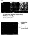
- Fig. 1 shows an orientation distribution of an embodiment of a typical Bi-Te based thermoelectric material according to the present invention as measured by EBSP analysis.
- Fig. 2 is an inverse pole figure of the thermoelectric material in the TD.
- EBSP analysis is carried out by irradiating a sample set in an SEM at a tilt angle of about 70° with an electron beam. The channeling pattern generated is observed on a computer screen to measure the orientation of the crystals at the irradiated site (see B.L. Adamus, S.I. Wright, and K. Kunze, Metall. Trans. A, 24A (1993), 819).
- thermoelectric material of the invention has a sea phase (matrix) composed of microcrytalline grains of 5 ⁇ m or smaller in which elongated islands (disperse phase) having an average length of 20 to 50 ⁇ m are distributed at random.
- the inverse pole figure of the TD in this field of vision indicates that the c-axis is aligned in the direction [0001] parallel with the pressing direction.
- the Bi-Te based thermoelectric material has a sea-island microstructure, in which the sea phase is composed of crystal grains having an average grain size of 5 ⁇ m or smaller and with their c-axes aligned unidirectionally, and the island phase is elongated crystal grains with an average length of 20 to 50 ⁇ m that are randomly distributed in the sea phase.
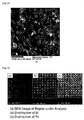
- Fig.3 is the results of EPMA on the surface of the thermoelectric material, which obviously show segregation of Te in the island phase.
- the crystal grains of the sea phase in the thermoelectric material preferably have an average size of 2 to 3 ⁇ m, and the crystal grains of the island phase preferably have an average length of 10 to 30 ⁇ m.
- the islands to sea ratio is preferably 20:80 to 50:50, more preferably 25:75 to 35:65.
- thermoelectric material was formed on the thermoelectric material by plasma spraying.
- a cross-sectional microstructure of the resulting sample is shown in Fig. 4 .
- a tensile force is exerted onto the thermoelectric material (element) by the residual stress generated in the thermal spray coating (A1 electrode). It is expected, therefore, that a crack easily occurs in the thermoelectric material near the interface with the electrode. However, no cracking occurs in the material near the material/electrode interface as demonstrated in Fig. 4 , proving that the material (element) suffers no delamination of the electrode.
- thermoelectric material of the present invention suffers no cracking near the interface with the electrode may be explained qualitatively as follows, which by no means limits the present invention.
- the Bi-Te based thermoelectric material has a sea-island microstructure.
- an Mo layer is previously formed on the surface of the thermoelectric material (element) non-uniformly to a thickness of about 50 ⁇ m to enhance the adhesion between the A1 electrode and the thermoelectric material (element).
- the islands randomly distributed in the microstructure of the thermoelectric material (element) strongly bind to the non-uniformly discretely distributed Mo layer (or Mo lumpy particles).
- thermoelectric element Since the thermoelectric element has a microstructure as if the Al electrode layer sets down hard roots in the thermoelectric material layer as mentioned above, the strength of the element is enhanced at and around the material-electrode interface. This is believed to be the reason the thermoelectric material (element) suffers no cracks near the material-electrode interface and so does not suffer from electrode delamination. This concept is depicted in Fig. 5 .
- thermoelectric material of the invention The process of producing the thermoelectric material of the invention will then be described. Powdered starting materials are weighed out and melted to prepare an ingot that becomes a material for sinter. The ingot is ground, reduced, and classified to obtain a sinter material. Separately, an ingot having a Te-rich composition (preferably with a Te content higher by 2 to 10 mol%, more preferably by 4 to 8 mol%, than the sinter material) is prepared by melting, which is similarly ground, reduced, and classified to obtain a Te-rich powder. The Te-rich powder is mixed into the sinter material. The mixed powder is packed into a press mold and sintered under pressure in a usual manner to obtain a sintered body. The Te-rich powder particles are believed to act as nuclei of a coarse island phase. The amount of the Te-rich powder to be mixed into 100 parts by mass of the sinter material is preferably 5 to 30 parts by mass, more preferably 8 to 20 parts by mass.
- Raw materials were weighed out to give an atomic ratio of Bi 2 Te 2.4 Se 0.6 , and 0.1 mass% SbI 3 was added thereto to adjust the carrier density.
- the mixed powder was vacuum sealed in an ampoule and melted while stirring at 650°C for 1 hour to obtain an ingot.
- the ingot was ground in a stamp mill and a ball mill and reduced at 390°C for 12 hours, followed by classification to obtain powder of 100 ⁇ m or smaller size as a sinter material.
- raw materials were weighted out at an atomic ratio of Bi 2 Te 3.0 Se 0.6 .
- the mixed powder was vacuum sealed in an ampoule and melted with stirring at 650°C for 1 hour to prepare a Te-rich ingot, which was ground in a stamp mill and a ball mill, reduced at 390°C for 12 hours, and classified to obtain powder of 100 ⁇ m or smaller.
- the powder was mixed into the above prepared sinter material at a ratio of 10 mass%.
- the resulting mixed sinter material was charged into a graphite die and hot pressed at 300 kgf/cm 2 , 410°C for 15 minutes to obtain a Bi-Te based thermoelectric material sintered body.
- the sintered body was cut and polished to prepare a sample for EBSP analysis.
- the orientation distribution and inverse polar figure were obtained by EBSP analysis.
- the results obtained are shown in Figs. 1 and 2 .
- the sintered body has a sea-island microstructure, in which the sea phase is composed of crystal grains having an average grain size of 5 ⁇ m or smaller and with the c-axes aligned unidirectionally, and the island phase is elongated crystal grains with an average length of 20 to 50 ⁇ m that are randomly distributed in the sea phase.
- the results of EPMA on the surface of the sintered body are shown in Fig. 3 , from which it is clear that Te is segregated in the islands.
- a specific heat capacity was obtained by DSC.
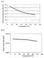
- a thermal conductivity was calculated from the thermal diffusivity, the specific heat capacity, and the density. The results are shown in Fig. 9 , which demonstrate that the Bi-Te based thermoelectric material has very low thermal conductivity.
- thermoelectric dimensionless figure of merit ZT as obtained from the power factor and the thermal conductivity values. It is confirmed that the thermoelectric material is superior in thermoelectric conversion performance with ZT>1 (at up to 425K).
- thermoelectric material A 4 mm wide, 20 mm long, and 3 mm thick test pieces cut out of the sintered body was subjected to three-point bending test. As a result, a strength value as high as 70 MPa or higher was obtained as shown in Fig. 11 . The fracture surface of the specimen after the testing is shown in Fig. 12 . The results demonstrate excellent mechanical strength of the thermoelectric material.
- thermoelectric material (element) surface has no cracking defects, involving no electrode delamination. It is apparent that the Al electrode is firmly joined to the thermoelectric material (element). It has now been confirmed that the thermoelectric material (element) of the invention suffers no cracking and so does not suffer electrode delamination in the production of thermoelectric modules.
- the thermoelectric materials (p type and n type elements) can therefore be connected in series normally to make thermoelectric modules.
- thermoelectric material sintered body was obtained in the same manner as in Example 1, except for using a sinter material prepared by grinding the ingot of the raw materials to powder of 50 ⁇ m or smaller in a ball mill, reducing the powder, and classifying to 50 ⁇ m or smaller (Te-rich powder was not added).
- Fig. 13 The sintered body of Comparative Example 1 was cut and polished to prepare a sample for EBSP analysis. The orientation distribution was obtained by EBSP analysis. The result is shown in Fig. 13 . It is seen that there is no sea-island microstructure but a microstructure composed of uniformly dispersed crystal grains of 50 ⁇ m or smaller.
- Fig. 14 is the results of EPMA on the surface of the sintered body, which show uniform distribution of the constituent elements.
- a 4 mm wide, 20 mm long, and 3 mm thick specimen cut out of the sintered body of Comparative Example 1 was subjected to three-point bending test.
- the fracture surface of the specimen after the testing is shown in Fig. 15 .
- the fracture surface of uniformly distributed grains of 50 ⁇ m or smaller is observed. Intergranular fracture is also observed in parts.
- An Al electrode was formed on the upper face of the cylinder by plasma spraying.
- the resulting sample was cut, embedded in a resin, and polished to observe the microstructure. The result is shown in Fig. 16 . It is seen that cracking has occurred on the thermoelectric material (element) surface to cause delamination of the electrode. Should such electrode delamination occur in even one of the electrodes making up a thermoelectric module, it will lead to immediate disconnection of the series circuit and death of the module.
- thermoelectric material according to the present invention has a sea-island texture in which islands are randomly distributed in the sea phase. At least one of the constituent elements is segregated in the islands.
- thermoelectric material element
- the process of producing a thermoelectric material according to the present invention provides, through relatively simple steps, a high performance thermoelectric material that does not undergo cracking due to the residual stress of thermal spraying and so does not suffer electrode delamination.
Landscapes
- Chemical & Material Sciences (AREA)
- Engineering & Computer Science (AREA)
- Mechanical Engineering (AREA)
- Materials Engineering (AREA)
- Metallurgy (AREA)
- Organic Chemistry (AREA)
- Manufacturing & Machinery (AREA)
- Inorganic Chemistry (AREA)
- Powder Metallurgy (AREA)
Applications Claiming Priority (2)
| Application Number | Priority Date | Filing Date | Title |
|---|---|---|---|
| JP2005275619A JP4876501B2 (ja) | 2005-09-22 | 2005-09-22 | 熱電変換材料及びその製造方法 |
| PCT/JP2006/315662 WO2007034632A1 (ja) | 2005-09-22 | 2006-08-08 | 熱電変換材料及びその製造方法 |
Publications (2)
| Publication Number | Publication Date |
|---|---|
| EP1928035A1 true EP1928035A1 (de) | 2008-06-04 |
| EP1928035A4 EP1928035A4 (de) | 2012-03-07 |
Family
ID=37888687
Family Applications (1)
| Application Number | Title | Priority Date | Filing Date |
|---|---|---|---|
| EP06782488A Withdrawn EP1928035A4 (de) | 2005-09-22 | 2006-08-08 | Thermoelektrisch umsetzendes material und prozess zu seiner herstellung |
Country Status (6)
| Country | Link |
|---|---|
| US (1) | US20090152492A1 (de) |
| EP (1) | EP1928035A4 (de) |
| JP (1) | JP4876501B2 (de) |
| CN (1) | CN100573948C (de) |
| CA (1) | CA2621115A1 (de) |
| WO (1) | WO2007034632A1 (de) |
Cited By (2)
| Publication number | Priority date | Publication date | Assignee | Title |
|---|---|---|---|---|
| MD323Z (ro) * | 2009-12-29 | 2011-08-31 | Институт Электронной Инженерии И Промышленных Технологий Академии Наук Молдовы | Microfir termoelectric în izolaţie de sticlă |
| WO2013144106A3 (de) * | 2012-03-29 | 2015-02-19 | Evonik Industries Ag | Pulvermetallurgische herstellung eines thermoelektrischen bauelements |
Families Citing this family (17)
| Publication number | Priority date | Publication date | Assignee | Title |
|---|---|---|---|---|
| JP5289451B2 (ja) * | 2008-08-28 | 2013-09-11 | 京セラ株式会社 | 熱電素子および熱電モジュール |
| KR101663183B1 (ko) | 2010-08-26 | 2016-10-06 | 삼성전자주식회사 | 열전재료, 이를 포함하는 열전모듈과 열전장치 |
| KR102065327B1 (ko) | 2012-03-21 | 2020-01-13 | 린텍 가부시키가이샤 | 열전 변환 재료 및 그 제조 방법 |
| KR101982279B1 (ko) | 2012-04-27 | 2019-08-28 | 삼성전자주식회사 | 고밀도 계면 미스핏 전위를 갖는 열전소재, 및 이를 구비한 열전소자와 열전모듈 |
| CN104211024B (zh) | 2013-06-04 | 2016-02-10 | 中国科学院上海硅酸盐研究所 | P型可逆相变高性能热电材料及其制备方法 |
| JP6277553B2 (ja) * | 2014-06-20 | 2018-02-14 | パナソニックIpマネジメント株式会社 | 熱電変換素子 |
| CN104218143B (zh) * | 2014-08-20 | 2017-06-13 | 中国航空工业集团公司北京航空材料研究院 | 一种BiAgSeTe基热电材料的制备方法 |
| CN104591103A (zh) * | 2014-12-30 | 2015-05-06 | 华中科技大学 | 一种Bi2Te3-xSx热电材料及其制备方法 |
| CN104555950B (zh) * | 2015-01-30 | 2017-02-22 | 中国科学院上海硅酸盐研究所 | 一种中温区具有优异热电性能的碲化铋材料及其制备方法 |
| KR101997203B1 (ko) * | 2015-07-21 | 2019-07-05 | 주식회사 엘지화학 | 화합물 반도체 열전 재료 및 그 제조방법 |
| PL3196951T3 (pl) | 2016-01-21 | 2019-07-31 | Evonik Degussa Gmbh | Racjonalny sposób wytwarzania elementów termoelektrycznych za pomocą metalurgii proszkowej |
| JP7209167B2 (ja) * | 2017-05-08 | 2023-01-20 | パナソニックIpマネジメント株式会社 | ジントル相熱電変換材料 |
| CN109873096A (zh) * | 2017-12-01 | 2019-06-11 | 中国电力科学研究院有限公司 | 一种温度可调控的车载动力电池组 |
| CN108172691B (zh) * | 2017-12-25 | 2019-09-03 | 电子科技大学 | 一种具有微结构的柔性热释电敏感薄膜的制备方法 |
| JP7314927B2 (ja) * | 2018-02-27 | 2023-07-26 | 住友化学株式会社 | 熱電変換モジュール用部材、熱電変換モジュール及び熱電変換モジュール用部材の製造方法 |
| US10714671B2 (en) * | 2018-05-18 | 2020-07-14 | Richard C Thuss | Apparatus, and process for cold spray deposition of thermoelectric semiconductor and other polycrystalline materials and method for making polycrystalline materials for cold spray deposition |
| US11411155B2 (en) | 2018-09-26 | 2022-08-09 | Hitachi Metals, Ltd. | Thermoelectric conversion material, thermoelectric conversion module using same, and method of manufacturing thermoelectric conversion material |
Family Cites Families (19)
| Publication number | Priority date | Publication date | Assignee | Title |
|---|---|---|---|---|
| GB950110A (en) * | 1960-05-14 | 1964-02-19 | Siemens Ag | Process for the production of sintered semi-conducting thermoelectric materials |
| US5981863A (en) * | 1995-03-03 | 1999-11-09 | Yamaha Corporation | Process of manufacturing thermoelectric refrigerator alloy having large figure of merit |
| CN1044422C (zh) * | 1995-12-10 | 1999-07-28 | 浙江大学 | 半导体热电材料的制造方法及设备 |
| JPH09172202A (ja) * | 1995-12-20 | 1997-06-30 | Aisin Seiki Co Ltd | 熱電素子 |
| US5763293A (en) * | 1996-03-04 | 1998-06-09 | Yamaha Corporation | Process of fabricating a thermoelectric module formed of V-VI group compound semiconductor including the steps of rapid cooling and hot pressing |
| JP3415391B2 (ja) * | 1996-05-01 | 2003-06-09 | ヤマハ株式会社 | 熱電材料の製造方法 |
| JP3909557B2 (ja) * | 1996-07-03 | 2007-04-25 | ヤマハ株式会社 | 熱電材料及びその製造方法 |
| EP1039556A4 (de) * | 1997-10-24 | 2007-02-21 | Neomax Co Ltd | Thermoelektrisches wandlermaterial und seine herstellung |
| TW405273B (en) * | 1998-04-23 | 2000-09-11 | Toyo Kohan Co Ltd | Manufacturing method of sintered material for thermo-electric converter elements, sintered materials for thermo-electric converter elements, and a thermoelectric converter element made by using the same |
| JP3603698B2 (ja) * | 1998-10-22 | 2004-12-22 | ヤマハ株式会社 | 熱電材料及び熱電変換素子 |
| JP4324999B2 (ja) * | 1998-11-27 | 2009-09-02 | アイシン精機株式会社 | 熱電半導体組成物及びその製造方法 |
| JP3600486B2 (ja) * | 1999-08-24 | 2004-12-15 | セイコーインスツル株式会社 | 熱電変換素子の製造方法 |
| CA2280990A1 (en) * | 1999-08-27 | 2001-02-27 | Jacques L'ecuyer | New process for producing thermoelectric alloys |
| JP3594008B2 (ja) * | 2000-11-30 | 2004-11-24 | ヤマハ株式会社 | 熱電材料、その製造方法及びペルチェモジュール |
| JP4273692B2 (ja) * | 2002-01-21 | 2009-06-03 | 宇部興産株式会社 | 熱電変換材料の製造方法 |
| JP2003243732A (ja) * | 2002-02-13 | 2003-08-29 | Komatsu Ltd | 熱電材料、及び、熱電材料の製造方法並びに製造装置 |
| JP2003243734A (ja) * | 2002-02-14 | 2003-08-29 | Mitsui Mining & Smelting Co Ltd | 熱電変換材料およびその製造方法 |
| JP2004134673A (ja) * | 2002-10-11 | 2004-04-30 | Mitsui Mining & Smelting Co Ltd | n型熱電変換材料およびその製造方法 |
| JP4286053B2 (ja) * | 2003-05-08 | 2009-06-24 | 株式会社Ihi | 熱電半導体材料、該熱電半導体材料による熱電半導体素子、該熱電半導体素子を用いた熱電モジュール及びこれらの製造方法 |
-
2005
- 2005-09-22 JP JP2005275619A patent/JP4876501B2/ja not_active Expired - Fee Related
-
2006
- 2006-08-08 CN CNB2006800329807A patent/CN100573948C/zh not_active Expired - Fee Related
- 2006-08-08 CA CA002621115A patent/CA2621115A1/en active Pending
- 2006-08-08 US US12/066,271 patent/US20090152492A1/en not_active Abandoned
- 2006-08-08 EP EP06782488A patent/EP1928035A4/de not_active Withdrawn
- 2006-08-08 WO PCT/JP2006/315662 patent/WO2007034632A1/ja not_active Ceased
Cited By (3)
| Publication number | Priority date | Publication date | Assignee | Title |
|---|---|---|---|---|
| MD323Z (ro) * | 2009-12-29 | 2011-08-31 | Институт Электронной Инженерии И Промышленных Технологий Академии Наук Молдовы | Microfir termoelectric în izolaţie de sticlă |
| WO2013144106A3 (de) * | 2012-03-29 | 2015-02-19 | Evonik Industries Ag | Pulvermetallurgische herstellung eines thermoelektrischen bauelements |
| US9530952B2 (en) | 2012-03-29 | 2016-12-27 | Evonik Industries Ag | Powder metallurgical production of a thermoelectric component |
Also Published As
| Publication number | Publication date |
|---|---|
| US20090152492A1 (en) | 2009-06-18 |
| WO2007034632A1 (ja) | 2007-03-29 |
| CA2621115A1 (en) | 2007-03-29 |
| CN100573948C (zh) | 2009-12-23 |
| CN101273474A (zh) | 2008-09-24 |
| JP4876501B2 (ja) | 2012-02-15 |
| EP1928035A4 (de) | 2012-03-07 |
| JP2007088239A (ja) | 2007-04-05 |
Similar Documents
| Publication | Publication Date | Title |
|---|---|---|
| US20090152492A1 (en) | Thermoelectric material and process of producing the same | |
| KR102165812B1 (ko) | 파마티나이트계 열전재료의 제조방법 | |
| EP2418923B1 (de) | Wärmeausdehnungsunterdrückungselement und Anti-Wärmeausdehnungselement | |
| KR101051010B1 (ko) | p형 Bi-Sb-Te계 열전재료의 제조방법 | |
| EP2913857B1 (de) | Thermoelektrisches mg-si-umwandlungsmaterial, verfahren zur herstellung davon, sinterkörper für thermoelektrische umwandlung, thermoelektrisches umwandlungselement und thermoelektrisches wandlermodul | |
| Santamaría et al. | Microcompression tests of single-crystalline and ultrafine grain Bi2Te3 thermoelectric material | |
| US20030168094A1 (en) | Thermoelectric material and process for manufacturing the same | |
| WO2013047474A1 (ja) | 焼結体、熱電変換素子用焼結体、熱電変換素子及び熱電変換モジュール | |
| Gonçalves et al. | Effect of Ni, Bi and Se on the tetrahedrite formation | |
| KR102198207B1 (ko) | 침입형 도핑재 첨가에 의한 복합결정구조가 형성된 Te계 열전소재 | |
| JP4854215B2 (ja) | 熱電材料とその製造方法 | |
| KR101631858B1 (ko) | 침입형 도핑재 첨가에 의해 복합결정구조가 형성된 Te계 열전재료 | |
| Schmidt et al. | Influence of silver nanoparticle addition, porosity, and processing technique on the mechanical properties of Ba0. 3Co4Sb12 skutterudites | |
| KR20170017214A (ko) | 산화아연이 혼합된 열전소재 및 그 제조방법 | |
| Rogl et al. | Thermoelectric Sb-based skutterudites for medium temperatures | |
| KR20190049016A (ko) | 테이프 캐스팅 공정을 이용한 결정배향된 칼코게나이드계 열전소재 및 이의 제조방법 | |
| JP2008028048A (ja) | カルシウム・コバルト層状酸化物単結晶からなる熱電材料の製造方法 | |
| Yuan et al. | Harnessing Phase‐Transition Hysteresis for Enhanced Thermoelectric Performance of Ductile Ag2 (S, Se, Te) | |
| Verges et al. | Young's Modulus and Hardness of Zr0. 5Hf0. 5Ni x Pd1–x Sn0. 99Sb0. 01 Half-Heusler Compounds | |
| US20240381772A1 (en) | Thermoelectric conversion material, composition for thermoelectric conversion material, thermoelectric conversion element, thermoelectric conversion module, thermoelectric conversion system, and method of manufacturing thermoelectric conversion material | |
| US20240381775A1 (en) | Thermoelectric conversion material, composition for thermoelectric conversion material, thermoelectric conversion element, thermoelectric conversion module, thermoelectric conversion system, and method of manufacturing thermoelectric conversion material | |
| JP3605366B2 (ja) | 熱電素子の製造方法及びそれを用いて製造した熱電素子並びに熱電モジュール | |
| JP2005223237A (ja) | 高強度熱電材料 | |
| CN114402445A (zh) | 热电转换元件、热电转换组件、接合材料、制造热电转换元件的方法 | |
| KR101825302B1 (ko) | 고온 접합성능이 우수한 전자부품 접합용 합금 및 그 페이스트 |
Legal Events
| Date | Code | Title | Description |
|---|---|---|---|
| PUAI | Public reference made under article 153(3) epc to a published international application that has entered the european phase |
Free format text: ORIGINAL CODE: 0009012 |
|
| 17P | Request for examination filed |
Effective date: 20080303 |
|
| AK | Designated contracting states |
Kind code of ref document: A1 Designated state(s): DE FR GB |
|
| RBV | Designated contracting states (corrected) |
Designated state(s): DE FR GB |
|
| A4 | Supplementary search report drawn up and despatched |
Effective date: 20120206 |
|
| RIC1 | Information provided on ipc code assigned before grant |
Ipc: H01L 35/26 20060101ALI20120131BHEP Ipc: H02N 11/00 20060101ALI20120131BHEP Ipc: C22C 1/04 20060101ALI20120131BHEP Ipc: C22C 12/00 20060101ALI20120131BHEP Ipc: C22C 30/00 20060101ALI20120131BHEP Ipc: H01L 35/34 20060101ALI20120131BHEP Ipc: H01L 35/16 20060101AFI20120131BHEP Ipc: B22F 3/14 20060101ALI20120131BHEP |
|
| STAA | Information on the status of an ep patent application or granted ep patent |
Free format text: STATUS: THE APPLICATION HAS BEEN WITHDRAWN |
|
| 18W | Application withdrawn |
Effective date: 20120417 |