EP1931095A1 - Lichtempfänger und verfahren zur erzeugung seines identifikationsschwellenwerts - Google Patents
Lichtempfänger und verfahren zur erzeugung seines identifikationsschwellenwerts Download PDFInfo
- Publication number
- EP1931095A1 EP1931095A1 EP05788349A EP05788349A EP1931095A1 EP 1931095 A1 EP1931095 A1 EP 1931095A1 EP 05788349 A EP05788349 A EP 05788349A EP 05788349 A EP05788349 A EP 05788349A EP 1931095 A1 EP1931095 A1 EP 1931095A1
- Authority
- EP
- European Patent Office
- Prior art keywords
- signal
- output
- circuit
- average
- amplifying unit
- Prior art date
- Legal status (The legal status is an assumption and is not a legal conclusion. Google has not performed a legal analysis and makes no representation as to the accuracy of the status listed.)
- Granted
Links
Images




Classifications
-
- H—ELECTRICITY
- H04—ELECTRIC COMMUNICATION TECHNIQUE
- H04L—TRANSMISSION OF DIGITAL INFORMATION, e.g. TELEGRAPHIC COMMUNICATION
- H04L25/00—Baseband systems
- H04L25/02—Details ; arrangements for supplying electrical power along data transmission lines
- H04L25/06—DC level restoring means; Bias distortion correction ; Decision circuits providing symbol by symbol detection
- H04L25/061—DC level restoring means; Bias distortion correction ; Decision circuits providing symbol by symbol detection providing hard decisions only; arrangements for tracking or suppressing unwanted low frequency components, e.g. removal of DC offset
-
- H—ELECTRICITY
- H03—ELECTRONIC CIRCUITRY
- H03G—CONTROL OF AMPLIFICATION
- H03G3/00—Gain control in amplifiers or frequency changers
- H03G3/20—Automatic control
- H03G3/30—Automatic control in amplifiers having semiconductor devices
- H03G3/3084—Automatic control in amplifiers having semiconductor devices in receivers or transmitters for electromagnetic waves other than radiowaves, e.g. lightwaves
-
- H—ELECTRICITY
- H04—ELECTRIC COMMUNICATION TECHNIQUE
- H04B—TRANSMISSION
- H04B10/00—Transmission systems employing electromagnetic waves other than radio-waves, e.g. infrared, visible or ultraviolet light, or employing corpuscular radiation, e.g. quantum communication
- H04B10/60—Receivers
- H04B10/66—Non-coherent receivers, e.g. using direct detection
- H04B10/69—Electrical arrangements in the receiver
- H04B10/693—Arrangements for optimizing the preamplifier in the receiver
- H04B10/6931—Automatic gain control of the preamplifier
-
- H—ELECTRICITY
- H04—ELECTRIC COMMUNICATION TECHNIQUE
- H04B—TRANSMISSION
- H04B10/00—Transmission systems employing electromagnetic waves other than radio-waves, e.g. infrared, visible or ultraviolet light, or employing corpuscular radiation, e.g. quantum communication
- H04B10/60—Receivers
- H04B10/66—Non-coherent receivers, e.g. using direct detection
- H04B10/69—Electrical arrangements in the receiver
- H04B10/695—Arrangements for optimizing the decision element in the receiver, e.g. by using automatic threshold control
Definitions
- the present invention relates to an optical receiver, and more particularly, to an optical receiver suitable for a passive-optical-network (PON) system that transmits a burst-like light signal and a discrimination-threshold generating method for the optical receiver.
- PON passive-optical-network
- the optical receiver includes a photoelectric conversion element, an automatic-threshold-control (ATC) circuit, and a discriminator.
- the photoelectric conversion element converts a received burst digital light signal into an electric signal; a preamplifier that outputs a first positive phase signal and a first negative phase signal with a differential output obtained by amplifying this electric signal to a predetermined level.
- the ATC circuit outputs a second positive phase signal and a second negative phase signal in a reverse-phase relation with the second positive phase signal, the second positive phase signal being obtained by averaging a value of the first positive phase signal and a value obtained by peak-holding the first negative phase signal and the second negative phase signal being obtained by averaging a value of the first negative phase signal and a value obtained by peak-holding the first positive phase signal at signal time or a value of an offset voltage set higher than this value at no-signal time.
- the discriminator decides, from the second positive phase signal and the second negative phase signal, a logical value "0" at the no-signal time of the burst digital light signal, and performs logical decision according to an intermediate value of amplitude values of the burst digital light signal and outputs logical values "1" and "0" at the signal time.
- the preamplifier connected to the photoelectric conversion element controls a gain of the preamplifier itself according to a detection level obtained by subjecting an optical output signal level from the photoelectric conversion element to peak detection at high speed.
- the auto threshold control circuit connected to an output side of the preamplifier inputs a discrimination output (level) to the discriminator at the post-stage.
- the discrimination output is obtained by averaging a signal output of a differential output signal outputted from the preamplifier and a selection circuit output generated based on two detection outputs obtained by performing peak detection (PD) and bottom detection (BD).
- Patent Document 1 Japanese Patent Application Laid-Open No. H9-181687 .
- the present invention has been devised in view of the above description and it is an object of the present invention to provide an optical receiver and a discrimination-threshold generating method for the optical receiver, which are capable of preventing unintended switching of a gain and generation of a wrong discrimination level even if there is a transient response in a light signal and generating a discrimination level equivalent to a discrimination level at the time when there is no transient response.
- an optical receiver includes a pre-amplifying unit that performs voltage conversion and amplification of an output of a light-receiving element to that receives a light signal and converts the light signal into a current signal; and a regenerating unit including a discriminating circuit that receives an output signal of the pre-amplifying unit as an input signal and performs a signal discrimination of the input signal based on a threshold generated based on the input signal.
- the pre-amplifying unit includes a first average detecting circuit that detects an average of output signals of the pre-amplifying unit, and controls an amplification gain of the pre-amplifying unit based on an output of comparison between an output of the first average detecting circuit and a predetermined reference voltage.
- the regenerating unit includes a second average detecting circuit that detects an average of input signals to the discriminating circuit, and outputs an output of the second average detecting circuit to the discriminating circuit as a threshold for signal discrimination of the input signal.
- the pre-amplifying unit controls an amplification gain of the pre-amplifying unit itself based on a comparative output of an output of the first average detecting circuit, which detects an average of output signals of the pre-amplifying unit itself, and the predetermined reference voltage.
- the regenerating unit outputs an output of the second average detecting circuit, which detects an average of input signals to the discriminating circuit, to the discriminating circuit as a threshold for performing signal discrimination of the input signals.
- Fig. 1 is a block diagram of a constitution of an optical receiver according to a first embodiment of the present invention.
- the optical receiver shown in the figure includes a light-receiving element 1 that receives a light signal, a pre-amplifying unit 2 that is inputted with an output current of the light-receiving element 1 and converts an inputted current signal into a voltage signal and outputs the voltage signal, and a regenerating unit 3 that is inputted with an output voltage of the pre-amplifying unit 2 and discriminates a voltage level of the output voltage inputted.
- the pre-amplifying unit 2 includes a transimpedance amplifier (TIA) 5 and an automatic-gain-control (AGC) unit 6.
- TIA transimpedance amplifier
- AGC automatic-gain-control
- the regenerating unit 3 includes an automatic-threshold-control (ATC) unit 7 that generates and outputs a predetermined threshold level and a discriminating circuit 18 that performs discrimination of an input signal (level) based on an input signal to the discriminating circuit 18 itself and an output of the ATC unit 7.
- ATC automatic-threshold-control
- the TIA 5 includes an inverting amplifier 12 and a feedback resistor (Rf) 13 and the AGC unit 6 includes an average detecting unit 14 that detects an average of output levels of the pre-amplifying unit 2, a comparing circuit 16 that compares an output level of the average detecting unit 14 and a reference voltage (Vref) 15, a feedback-resistor (Rf) driving unit 17 that variably controls a resistance of the feedback resistor (Rf), and the feedback resistor (Rf) 13.
- Vref reference voltage
- Rf feedback-resistor
- the feedback resistor 13 Since the feedback resistor 13 has both a conversion action of converting a current signal into a voltage signal and a gain control action for the inverting amplifier 12, the feedback resistor 13 is included in the respective components, the TIA 5 and the AGC unit 6, as described above.
- a light signal received by the light-receiving element 1 is converted into a current signal. Then, the light signal is converted into a voltage signal and amplified by the TIA 5. Thereafter, an average of output amplitudes is continuously detected by the average detecting unit 14 serving as a first average detecting circuit. A differential voltage between the average and the reference voltage 15 is generated by the comparing circuit 16.
- the feedback-resistor driving unit 17 drives (variably controls) a value of the feedback resistor 13 based on an output signal of the comparing circuit 16. According to such control, for example, when an output amplitude of the TIA 5 is larger than the reference voltage 15, an AGC control is performed to reduce the output amplitude to an amplitude determined by the reference voltage 15.
- a predetermined threshold voltage is generated and outputted by an average detecting unit 19, which serves as a second average detecting circuit, as an output from the ATC unit 7 to the discriminating circuit 18.
- the regeneration processing is performed based on a discrimination level according to light-receiving power of the light-receiving element 1.
- FIG. 2A is a diagram for explaining an operation (an ideal operation at the time when a transient response is not taken into account) in the optical receiver to which the conventional technology is applied.
- an optical receiver having a general constitution, to which the conventional technology is applied is assumed.
- (a) is a diagram of an ideal light signal waveform at the time when a transient response is not taken into account (it is assumed that there is no transient response).
- this light signal is converted into a current signal by a light-receiving element and inputted to a pre-amplifying unit, since a leading pulse of a burst signal exceeds a level (a level 1) at the time when the AGC operates, an AGC gain is instantly reduced to limit an output amplitude ((b) in the figure).
- the ATC operates and a threshold level for discrimination is set to an intermediate level between an upper limit level (a "High” level) and a lower limit level (a "Low” level) of a signal pulse ((c) in the figure).
- a threshold level for discrimination is set to an intermediate level between an upper limit level (a "High” level) and a lower limit level (a "Low” level) of a signal pulse ((c) in the figure).
- the AGC unit operates when gain switching is necessary and the ATC unit also operates to generate a discrimination level corresponding to an amplitude of an input signal to the ATC unit itself. Therefore, it can be said that, in the optical receiver having the general constitution to which the conventional technology is applied, it is difficult to find presence of a problem insofar as the operation at the time when there is no transient response is considered.
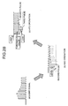
- Fig. 2B is a diagram for explaining an operation in the optical receiver, to which the conventional technology is applied, at the time when a transient response is taken into account.
- (a) is a diagram of a light signal waveform at the time when a transient response is taken into account.
- this light signal is converted into a current signal by the light-receiving element and inputted to the pre-amplifying unit, in an example shown in (b) in the figure, since a second pulse of a burst signal exceeds the level (the level 1) at the time when the AGC unit operates, an AGC gain is reduced to limit an output amplitude.
- a waveform indicated by a solid line is a waveform at the time when AGC operates.
- a waveform indicated by a wavy line is a waveform at the time when it is assumed that the AGC unit does not operate.
- a part indicated by (c) is a waveform showing an output signal of the pre-amplifying unit at the time when the AGC does not operate.
- a threshold level for discrimination is set to, for example, an intermediate level between an upper limit level (a "High” level) and a lower limit level (a "Low” level) of a third pulse of the burst signal.
- a threshold level is set, a seventh pulse and the subsequent pulses of the burst signal inputted to the regenerating unit are discriminated by mistake.
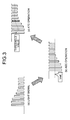
- Fig. 3 is a diagram for explaining an operation in the optical receiver in the first embodiment at the time when a transient response is taken into account.
- FIG. 3 (a) is a diagram of a light signal waveform at the time when a transient response similar to (a) shown in Fig. 2B is taken into account.
- this light signal is converted into a current signal by the light-receiving element 1 in Fig. 1 and inputted to the pre-amplifying unit 2, for example, as (b) shown in Fig. 3 .
- an average output from the average detecting unit 14, which is the other input signal inputted to the comparing circuit 16 does not exceed the reference voltage 15 or an amount of decrease in an AGC gain is small even if the average output exceeds the reference voltage 15.
- AGC rarely acts and a signal waveform of a light-receiving output signal is maintained. As a result, unintended gain switching in the AGC unit is prevented.
- a signal waveform of (b) shown in Fig. 3 is inputted to the regenerating unit 3 as an output waveform of the pre-amplifying unit 2.
- the average detecting unit 19 of the ATC unit 7 operates and a threshold level for discrimination is set to an intermediate level between upper limit levels ("High” levels) and lower limit levels ("Low” levels) of respective pulses of the burst signal. Therefore, since the threshold level follows substantially a median (an average) of the upper limit levels and the lower limit levels of the respective pulses, a threshold level that does not cause an error in regeneration processing is generated.
- the pre-amplifying unit controls an amplification gain of the pre-amplifying unit itself based on a comparative output of an output of the first average detecting circuit, which detects an average of output signals of the pre-amplifying unit itself, and a predetermined reference voltage.
- the regenerating unit outputs an output of the second average detecting circuit, which detects an average of input signals to the discriminating circuit, to the discriminating circuit as a threshold for performing signal discrimination of the input signals.
- a gain of the TIA that is, a gain of the pre-amplifying unit is controlled based on feedback resistance control of the feedback resistor driving unit.
- the present invention is not limited to this constitution. Any constitution is included in the present invention as long as, for example, it is possible to control a gain of the pre-amplifying unit based on a result of comparison between the average detecting unit and the predetermined reference voltage.
- Fig. 4 is a block diagram of a constitution of an optical receiver according to a second embodiment of the present invention.
- the regenerating unit 3 of the optical receiver shown in the figure includes a discriminating circuit 21 that outputs a positive phase output and a negative phase output instead of the discriminating circuit 21 according to the first embodiment.
- the regenerating unit 3 further includes a comparing circuit 22 serving as a second comparing circuit that generates a differential voltage between both the phase outputs of the discriminating circuit 21, a sample-and-hold (S/H) circuit 23 that decides, based on a signal level of a control signal 24, whether an output (the differential voltage) of the comparing circuit 22 should be held or outputted to a circuit at the next stage, and an offset adjusting circuit 25 that outputs an offset adjusting signal generated based on an output of the S/H circuit 23 to the ATC unit 7.
- the ATC unit 7 further includes a buffer unit 12 that is connected to an output side of the average detecting unit 19 in the constitution of the first embodiment and to which the output (the offset adjusting signal) of the offset adjusting circuit 25 is inputted.
- An output of the buffer unit 26 is inputted to the discriminating circuit 21.
- the other components of the optical receiver are identical with or equivalent to those in the first embodiment shown in Fig. 1 .
- the components are denoted by the identical reference numerals. Explanations of the components are omitted. In the following explanation, operations different from those in the first embodiment are mainly explained.
- the operation is different from that in the first embodiment in that an initial offset of the regenerating unit 3 is automatically adjusted to be minimized.
- the comparing circuit 22 generates a differential voltage between a positive phase output and a negative phase output of the discriminating circuit 21 and outputs the differential voltage to the S/H circuit 23.
- the control signal 24 is inputted to the S/H circuit 23.
- the control signal 24 designates operation modes of the S/H circuit 23 including a sample mode and a hold mode. When a signal level of the control signal 24 designates the hold mode, the S/H circuit 23 holds a sampled voltage.
- the S/H circuit 23 When a signal level of the control signal 24 designates the sample mode, the S/H circuit 23 outputs a sampled voltage to the offset adjusting circuit 25.
- the sampled voltage is outputted to the offset adjusting circuit 25, an output voltage of the buffer unit 26 of the ATC unit 7 is changed based on the output of the offset adjusting circuit 25.
- a feedback loop for reducing a voltage difference between a positive phase output and a negative phase output of a discriminating circuit to nearly zero acts on the discriminating circuit 21. Circuit offset components of the discriminating circuit 21 and the ATC unit 7 are canceled. Sensitivity fluctuation of the optical receiver itself is reduced by this operation.
- an offset component included in an output of the second average circuit is controlled based on an output of the sample-and-hold circuit that holds or transmits a comparative output obtained by comparing respective differential outputs of the discriminating circuit.
- feedback control for reducing a voltage difference between differential outputs of the discriminating circuit to nearly zero is performed. It is possible to reduce sensitivity fluctuation of the optical receiver itself.
- Fig. 5 is a diagram for explaining an operation of an optical receiver according to a third embodiment of the present invention.
- (a) is a burst signal having a light signal waveform in which a transient response occurs; and (b) is respective outputs of the optical receiver.
- a solid line section indicates, for example, a positive phase output of the discriminating circuit 21.
- a broken line section indicates, for example, a negative phase output of the discriminating circuit 21.
- a part indicated by (c) is an example of a control signal waveform of the control signal 24 inputted to the S/H circuit 23.
- a characteristic of the third embodiment resides in an output form of the control signal 24 indicated by ⁇ shown in Fig. 5 .
- the control signal 24 for setting an operation mode of the S/H circuit 23 in the sample mode only in a non-signal period after application of a power supply is outputted. Therefore, an output offset in the non-signal period after application of a power supply is minimized. Since the output offset in the non-signal period after application of a power supply is minimized, it is possible to maintain minimized state of the output offset even in non-signal periods (in an example in Fig. 5 , a first packet interval between a first packet and a second packet and a second packet interval after the second packet) similar to the non-signal period after application of a power supply.
- Fig. 6 is a diagram for explaining an operation of an optical receiver according to a fourth embodiment of the present invention.
- an operation mode of the S/H circuit 23 is designated to be the sample mode only in the non-signal period after application of a power supply.
- an operation mode of the S/H circuit 23 is designated to be the sample mode in all no-signal areas of a light signal.
- the non-signal period after application of a power supply is set to be in the hold mode. It goes without saying that an operation mode in this period may be set to be the sample mode.
- the operation mode of the S/H circuit 23 is set in the sample mode in all the no-signal areas of a light signal.
- accumulation of output offset components is prevented. This makes it possible to reduce deterioration over time or aged deterioration in offset components.
- the offset control by the offset adjusting circuit is performed in non-signal periods among light signals.
- the offset control by the offset adjusting circuit is performed in non-signal periods among light signals.
- the optical receiver according to the prevent invention is useful for, for example, a PON system that transmits a burst-like light signal and suitable, in particular, when a transient response of an input signal becomes a problem.
Landscapes
- Engineering & Computer Science (AREA)
- Computer Networks & Wireless Communication (AREA)
- Signal Processing (AREA)
- Physics & Mathematics (AREA)
- Electromagnetism (AREA)
- Power Engineering (AREA)
- Optical Communication System (AREA)
- Dc Digital Transmission (AREA)
Applications Claiming Priority (1)
| Application Number | Priority Date | Filing Date | Title |
|---|---|---|---|
| PCT/JP2005/017812 WO2007036993A1 (ja) | 2005-09-28 | 2005-09-28 | 光受信器およびその識別閾値生成方法 |
Publications (3)
| Publication Number | Publication Date |
|---|---|
| EP1931095A1 true EP1931095A1 (de) | 2008-06-11 |
| EP1931095A4 EP1931095A4 (de) | 2010-04-28 |
| EP1931095B1 EP1931095B1 (de) | 2012-01-18 |
Family
ID=37899432
Family Applications (1)
| Application Number | Title | Priority Date | Filing Date |
|---|---|---|---|
| EP05788349A Expired - Lifetime EP1931095B1 (de) | 2005-09-28 | 2005-09-28 | Lichtempfänger und verfahren zur erzeugung seines identifikationsschwellenwerts |
Country Status (6)
| Country | Link |
|---|---|
| US (1) | US7609980B2 (de) |
| EP (1) | EP1931095B1 (de) |
| JP (1) | JP4532563B2 (de) |
| CN (1) | CN101243663B (de) |
| TW (1) | TWI327835B (de) |
| WO (1) | WO2007036993A1 (de) |
Families Citing this family (24)
| Publication number | Priority date | Publication date | Assignee | Title |
|---|---|---|---|---|
| JP4503624B2 (ja) * | 2006-03-30 | 2010-07-14 | 住友電工デバイス・イノベーション株式会社 | 電子回路 |
| US7601940B2 (en) * | 2007-03-22 | 2009-10-13 | Avago Technologies Ecbu Ip (Singapore) Pte. Ltd. | Gain control system for visible light communication systems |
| JP5028179B2 (ja) * | 2007-08-03 | 2012-09-19 | 株式会社日立製作所 | Ponシステム |
| CN101651497B (zh) * | 2008-08-13 | 2013-10-09 | 华为技术有限公司 | 光接收机增益控制方法和的光接收装置 |
| JP2010093353A (ja) * | 2008-10-03 | 2010-04-22 | Sumitomo Electric Ind Ltd | 光受信器 |
| EP2388933A4 (de) * | 2009-01-19 | 2014-06-25 | Hitachi Ltd | Transimpedanzverstärker und pon-system |
| JP5481240B2 (ja) * | 2010-03-12 | 2014-04-23 | 株式会社日立製作所 | マルチレート用バーストモード受信機 |
| JP5480010B2 (ja) * | 2010-05-14 | 2014-04-23 | 株式会社東芝 | 光受信回路 |
| WO2012137299A1 (ja) | 2011-04-05 | 2012-10-11 | 三菱電機株式会社 | 光受信器 |
| CN102412906A (zh) * | 2011-08-08 | 2012-04-11 | 中兴通讯股份有限公司 | 差分四相相移键控接收机及其增益控制方法 |
| JP5921130B2 (ja) * | 2011-10-12 | 2016-05-24 | アズビル株式会社 | 光電センサ |
| JP5894869B2 (ja) * | 2012-06-21 | 2016-03-30 | 株式会社日立製作所 | トランスインピーダンスアンプ |
| US9450542B2 (en) * | 2013-01-16 | 2016-09-20 | Mitsubishi Electric Corporation | Preamplifier, optical receiver, optical termination device, and optical communication system |
| US9325426B2 (en) * | 2013-07-11 | 2016-04-26 | Avago Technologies General Ip (Singapore) Pte. Ltd. | Burst-mode receiver having a wide dynamic range and low pulse-width distortion and a method |
| DE102014109716B4 (de) * | 2013-07-11 | 2017-11-16 | Avago Technologies General Ip (Singapore) Pte. Ltd. | Ein Stossbetriebsempfänger, welcher einen großen Dynamikbereich und niedrige Pulsweitenverzerrung hat und ein Verfahren |
| JP6443194B2 (ja) * | 2015-04-13 | 2018-12-26 | 富士通株式会社 | 信号識別回路、これを用いた光受信器、及び信号識別方法 |
| US10481246B2 (en) * | 2017-05-22 | 2019-11-19 | Analog Devices Global Unlimited Company | Photo-diode emulator circuit for transimpedance amplifier testing |
| US11005573B2 (en) * | 2018-11-20 | 2021-05-11 | Macom Technology Solutions Holdings, Inc. | Optic signal receiver with dynamic control |
| CN114175531B (zh) * | 2019-08-09 | 2024-03-22 | 三菱电机株式会社 | 光接收器和站侧装置 |
| TWI687048B (zh) * | 2019-11-04 | 2020-03-01 | 茂達電子股份有限公司 | 高線性光感測器 |
| US12013423B2 (en) | 2020-09-30 | 2024-06-18 | Macom Technology Solutions Holdings, Inc. | TIA bandwidth testing system and method |
| US11658630B2 (en) | 2020-12-04 | 2023-05-23 | Macom Technology Solutions Holdings, Inc. | Single servo loop controlling an automatic gain control and current sourcing mechanism |
| US11381318B1 (en) * | 2021-07-30 | 2022-07-05 | II-VI Delaware, Inc | Control of trans-impedance amplifier (TIA) during settling after recovering from loss of signal in receiver |
| CN114088346B (zh) * | 2021-11-29 | 2025-01-21 | 桂林聚联科技有限公司 | 一种光纤时延测量装置 |
Family Cites Families (16)
| Publication number | Priority date | Publication date | Assignee | Title |
|---|---|---|---|---|
| JPH01188143A (ja) * | 1988-01-22 | 1989-07-27 | Nec Corp | 光受信器の識別回路 |
| JPH01286655A (ja) * | 1988-05-13 | 1989-11-17 | Sumitomo Electric Ind Ltd | 光受信回路 |
| JP3418654B2 (ja) * | 1995-10-27 | 2003-06-23 | 株式会社日立製作所 | プリアンプ |
| JP2723874B2 (ja) | 1995-12-26 | 1998-03-09 | 日本電気エンジニアリング株式会社 | バーストディジタル光受信器 |
| JP2814990B2 (ja) | 1996-05-20 | 1998-10-27 | 日本電気株式会社 | 光受信回路 |
| GB2328816B (en) * | 1997-08-30 | 2002-05-08 | Siemens Plc | Optical data communications receiver |
| US5907261A (en) * | 1997-09-05 | 1999-05-25 | Ericsson Inc. | Method and apparatus for controlling signal amplitude level |
| JP3979712B2 (ja) * | 1997-10-20 | 2007-09-19 | 富士通株式会社 | 光信号受信装置および方法 |
| JP2000216733A (ja) * | 1997-11-28 | 2000-08-04 | Kokusai Electric Co Ltd | 光電気変換方法及び受光回路及び光通信システム |
| JP4019555B2 (ja) * | 1999-05-25 | 2007-12-12 | Kddi株式会社 | 光受信装置及び方法 |
| JP3475877B2 (ja) * | 1999-10-25 | 2003-12-10 | 日本電気株式会社 | 前置増幅回路 |
| WO2001048914A1 (en) * | 1999-12-27 | 2001-07-05 | Fujitsu Limited | Signal amplifying circuit and optical signal receiver using the same |
| JP2001197049A (ja) * | 2000-01-14 | 2001-07-19 | Fujitsu Ltd | クロック再生回路及びこれを用いた光信号受信器 |
| US6785344B1 (en) * | 2000-04-11 | 2004-08-31 | Terawave Communications, Inc. | Fast threshold determination for packet-multiplexed digital communication |
| US7058315B2 (en) * | 2001-10-09 | 2006-06-06 | Chiaro Networks Ltd. | Fast decision threshold controller for burst-mode receiver |
| US6844784B1 (en) * | 2002-11-26 | 2005-01-18 | Finisar Corporation | Wide dynamic range transimpedance amplifier |
-
2005
- 2005-09-28 WO PCT/JP2005/017812 patent/WO2007036993A1/ja not_active Ceased
- 2005-09-28 US US10/585,458 patent/US7609980B2/en not_active Expired - Fee Related
- 2005-09-28 JP JP2007537493A patent/JP4532563B2/ja not_active Expired - Fee Related
- 2005-09-28 CN CN200580002707.5A patent/CN101243663B/zh not_active Expired - Fee Related
- 2005-09-28 EP EP05788349A patent/EP1931095B1/de not_active Expired - Lifetime
-
2006
- 2006-08-31 TW TW095132130A patent/TWI327835B/zh not_active IP Right Cessation
Also Published As
| Publication number | Publication date |
|---|---|
| JPWO2007036993A1 (ja) | 2009-04-02 |
| JP4532563B2 (ja) | 2010-08-25 |
| CN101243663A (zh) | 2008-08-13 |
| US20070098416A1 (en) | 2007-05-03 |
| EP1931095B1 (de) | 2012-01-18 |
| TW200713873A (en) | 2007-04-01 |
| CN101243663B (zh) | 2011-04-13 |
| US7609980B2 (en) | 2009-10-27 |
| TWI327835B (en) | 2010-07-21 |
| WO2007036993A1 (ja) | 2007-04-05 |
| EP1931095A4 (de) | 2010-04-28 |
Similar Documents
| Publication | Publication Date | Title |
|---|---|---|
| US7609980B2 (en) | Optical receiver and discrimination-threshold generating method | |
| US8150272B2 (en) | Systems and methods for transferring single-ended burst signal onto differential lines, especially for use in burst-mode receiver | |
| US20060126683A1 (en) | Optical transmitter having analog/digital mixed-mode temperature compensation function | |
| EP2096754B1 (de) | Optische empfänger | |
| JP3749718B2 (ja) | バーストモード光受信機 | |
| JP2003332988A (ja) | バーストモード光受信機の判別しきい値制御装置 | |
| US5517351A (en) | Optical receiver apparatus | |
| EP1355437A1 (de) | Niedrigstwertdektor für einen optischen Empfänger im Burstbetrieb | |
| EP1717972B1 (de) | Automatische bitratensteuerschaltung | |
| CN114175531A (zh) | 光接收器和站侧装置 | |
| KR101519443B1 (ko) | 광 수신기 | |
| JP6661057B1 (ja) | リミッティング増幅回路 | |
| US8144813B2 (en) | Receiving method and receiving circuit | |
| KR20040084623A (ko) | 버스트 모드 광 수신 장치 | |
| EP2391003A1 (de) | Linearer Burstmodusempfänger | |
| JP4760312B2 (ja) | 光受信器 | |
| KR100847977B1 (ko) | 광 수신기 및 그의 식별 임계값 생성 방법 | |
| EP1322082A1 (de) | Geichstromvorspannung Schaltung für einen optischen Empfänger | |
| EP1935091B1 (de) | Systeme und verfahren zum transferieren eines asymmetrischen burst-signals auf differenzleitungen insbesondere für die verwendung in einem burst-modus-empfänger | |
| JP2010161623A (ja) | 光バースト受信器、及び、方法 | |
| KR102938846B1 (ko) | 펄스진폭변조 시스템 응용을 위한 자동이득 조절이 가능한 버스트모드 광 수신기 및 방법 | |
| EP0782264A2 (de) | Digitaler Empfänger mit adaptiven Schwellenwerten | |
| JP2011023936A (ja) | 光受信回路及び振幅判定器 | |
| JP2007266726A (ja) | 受信器を搭載した電子装置 | |
| JPH05268272A (ja) | 信号識別方法 |
Legal Events
| Date | Code | Title | Description |
|---|---|---|---|
| PUAI | Public reference made under article 153(3) epc to a published international application that has entered the european phase |
Free format text: ORIGINAL CODE: 0009012 |
|
| 17P | Request for examination filed |
Effective date: 20060824 |
|
| AK | Designated contracting states |
Kind code of ref document: A1 Designated state(s): DE FR GB IT |
|
| RBV | Designated contracting states (corrected) |
Designated state(s): DE FR GB IT |
|
| RBV | Designated contracting states (corrected) |
Designated state(s): DE FR GB IT |
|
| A4 | Supplementary search report drawn up and despatched |
Effective date: 20100329 |
|
| RIC1 | Information provided on ipc code assigned before grant |
Ipc: H04L 25/06 20060101ALI20100323BHEP Ipc: H04L 25/03 20060101ALI20100323BHEP Ipc: H03G 3/30 20060101ALI20100323BHEP Ipc: H04B 10/158 20060101AFI20100323BHEP |
|
| RIC1 | Information provided on ipc code assigned before grant |
Ipc: H03G 3/30 20060101ALI20110407BHEP Ipc: H04L 25/03 20060101ALI20110407BHEP Ipc: H04B 10/158 20060101AFI20110407BHEP Ipc: H04L 25/06 20060101ALI20110407BHEP |
|
| GRAP | Despatch of communication of intention to grant a patent |
Free format text: ORIGINAL CODE: EPIDOSNIGR1 |
|
| DAX | Request for extension of the european patent (deleted) | ||
| GRAS | Grant fee paid |
Free format text: ORIGINAL CODE: EPIDOSNIGR3 |
|
| GRAA | (expected) grant |
Free format text: ORIGINAL CODE: 0009210 |
|
| RAP1 | Party data changed (applicant data changed or rights of an application transferred) |
Owner name: MITSUBISHI ELECTRIC CORPORATION |
|
| AK | Designated contracting states |
Kind code of ref document: B1 Designated state(s): DE FR GB IT |
|
| REG | Reference to a national code |
Ref country code: GB Ref legal event code: FG4D |
|
| REG | Reference to a national code |
Ref country code: DE Ref legal event code: R096 Ref document number: 602005032305 Country of ref document: DE Effective date: 20120315 |
|
| PLBE | No opposition filed within time limit |
Free format text: ORIGINAL CODE: 0009261 |
|
| STAA | Information on the status of an ep patent application or granted ep patent |
Free format text: STATUS: NO OPPOSITION FILED WITHIN TIME LIMIT |
|
| PG25 | Lapsed in a contracting state [announced via postgrant information from national office to epo] |
Ref country code: IT Free format text: LAPSE BECAUSE OF FAILURE TO SUBMIT A TRANSLATION OF THE DESCRIPTION OR TO PAY THE FEE WITHIN THE PRESCRIBED TIME-LIMIT Effective date: 20120118 |
|
| 26N | No opposition filed |
Effective date: 20121019 |
|
| REG | Reference to a national code |
Ref country code: DE Ref legal event code: R097 Ref document number: 602005032305 Country of ref document: DE Effective date: 20121019 |
|
| REG | Reference to a national code |
Ref country code: DE Ref legal event code: R084 Ref document number: 602005032305 Country of ref document: DE |
|
| REG | Reference to a national code |
Ref country code: GB Ref legal event code: 746 Effective date: 20140325 |
|
| REG | Reference to a national code |
Ref country code: DE Ref legal event code: R079 Ref document number: 602005032305 Country of ref document: DE Free format text: PREVIOUS MAIN CLASS: H04B0010158000 Ipc: H04B0010660000 |
|
| REG | Reference to a national code |
Ref country code: DE Ref legal event code: R084 Ref document number: 602005032305 Country of ref document: DE Effective date: 20140326 Ref country code: DE Ref legal event code: R079 Ref document number: 602005032305 Country of ref document: DE Free format text: PREVIOUS MAIN CLASS: H04B0010158000 Ipc: H04B0010660000 Effective date: 20140610 Ref country code: DE Ref legal event code: R079 Ref document number: 602005032305 Country of ref document: DE Free format text: PREVIOUS MAIN CLASS: H04L0025030000 Ipc: H04B0010158000 Effective date: 20110407 |
|
| REG | Reference to a national code |
Ref country code: FR Ref legal event code: PLFP Year of fee payment: 12 |
|
| PGFP | Annual fee paid to national office [announced via postgrant information from national office to epo] |
Ref country code: DE Payment date: 20160920 Year of fee payment: 12 Ref country code: GB Payment date: 20160928 Year of fee payment: 12 |
|
| PGFP | Annual fee paid to national office [announced via postgrant information from national office to epo] |
Ref country code: FR Payment date: 20160816 Year of fee payment: 12 |
|
| REG | Reference to a national code |
Ref country code: DE Ref legal event code: R119 Ref document number: 602005032305 Country of ref document: DE |
|
| GBPC | Gb: european patent ceased through non-payment of renewal fee |
Effective date: 20170928 |
|
| REG | Reference to a national code |
Ref country code: FR Ref legal event code: ST Effective date: 20180531 |
|
| PG25 | Lapsed in a contracting state [announced via postgrant information from national office to epo] |
Ref country code: GB Free format text: LAPSE BECAUSE OF NON-PAYMENT OF DUE FEES Effective date: 20170928 Ref country code: DE Free format text: LAPSE BECAUSE OF NON-PAYMENT OF DUE FEES Effective date: 20180404 |
|
| PG25 | Lapsed in a contracting state [announced via postgrant information from national office to epo] |
Ref country code: FR Free format text: LAPSE BECAUSE OF NON-PAYMENT OF DUE FEES Effective date: 20171002 |