EP1933373A2 - Verfahren zur Herstellung einer Vorrichtung auf der Grundlage von Nanokristallen, die mit einer Nitridschicht beschichtet sind, die durch chemische Dampfabscheidung (CVD) aufgebracht wurde - Google Patents
Verfahren zur Herstellung einer Vorrichtung auf der Grundlage von Nanokristallen, die mit einer Nitridschicht beschichtet sind, die durch chemische Dampfabscheidung (CVD) aufgebracht wurde Download PDFInfo
- Publication number
- EP1933373A2 EP1933373A2 EP07122702A EP07122702A EP1933373A2 EP 1933373 A2 EP1933373 A2 EP 1933373A2 EP 07122702 A EP07122702 A EP 07122702A EP 07122702 A EP07122702 A EP 07122702A EP 1933373 A2 EP1933373 A2 EP 1933373A2
- Authority
- EP
- European Patent Office
- Prior art keywords
- nanocrystals
- nitride
- precursor gas
- deposition
- silicon
- Prior art date
- Legal status (The legal status is an assumption and is not a legal conclusion. Google has not performed a legal analysis and makes no representation as to the accuracy of the status listed.)
- Ceased
Links
- 239000002159 nanocrystal Substances 0.000 title claims abstract description 137
- 150000004767 nitrides Chemical class 0.000 title claims abstract description 49
- 238000004519 manufacturing process Methods 0.000 title abstract description 5
- 239000007789 gas Substances 0.000 claims abstract description 61
- 239000002243 precursor Substances 0.000 claims abstract description 55
- 238000000151 deposition Methods 0.000 claims abstract description 49
- 238000000034 method Methods 0.000 claims abstract description 47
- 230000008021 deposition Effects 0.000 claims abstract description 46
- 238000002161 passivation Methods 0.000 claims abstract description 42
- 230000015654 memory Effects 0.000 claims abstract description 38
- 230000015572 biosynthetic process Effects 0.000 claims abstract description 31
- 238000005229 chemical vapour deposition Methods 0.000 claims abstract description 30
- 239000000463 material Substances 0.000 claims abstract description 30
- 239000000758 substrate Substances 0.000 claims abstract description 26
- 239000004065 semiconductor Substances 0.000 claims abstract description 25
- 239000000203 mixture Substances 0.000 claims abstract description 17
- 239000003989 dielectric material Substances 0.000 claims abstract description 16
- XUIMIQQOPSSXEZ-UHFFFAOYSA-N Silicon Chemical group [Si] XUIMIQQOPSSXEZ-UHFFFAOYSA-N 0.000 claims description 55
- 229910052710 silicon Inorganic materials 0.000 claims description 54
- 239000010703 silicon Substances 0.000 claims description 54
- 230000035784 germination Effects 0.000 claims description 27
- 230000008569 process Effects 0.000 claims description 20
- 229910052581 Si3N4 Inorganic materials 0.000 claims description 17
- HQVNEWCFYHHQES-UHFFFAOYSA-N silicon nitride Chemical compound N12[Si]34N5[Si]62N3[Si]51N64 HQVNEWCFYHHQES-UHFFFAOYSA-N 0.000 claims description 17
- 238000007667 floating Methods 0.000 claims description 16
- VYPSYNLAJGMNEJ-UHFFFAOYSA-N Silicium dioxide Chemical compound O=[Si]=O VYPSYNLAJGMNEJ-UHFFFAOYSA-N 0.000 claims description 14
- MROCJMGDEKINLD-UHFFFAOYSA-N dichlorosilane Chemical compound Cl[SiH2]Cl MROCJMGDEKINLD-UHFFFAOYSA-N 0.000 claims description 13
- 229910052814 silicon oxide Inorganic materials 0.000 claims description 12
- BLRPTPMANUNPDV-UHFFFAOYSA-N Silane Chemical compound [SiH4] BLRPTPMANUNPDV-UHFFFAOYSA-N 0.000 claims description 10
- 229910000077 silane Inorganic materials 0.000 claims description 10
- QGZKDVFQNNGYKY-UHFFFAOYSA-N Ammonia Chemical compound N QGZKDVFQNNGYKY-UHFFFAOYSA-N 0.000 claims description 8
- 229910021529 ammonia Inorganic materials 0.000 claims description 4
- 229910052732 germanium Inorganic materials 0.000 claims description 4
- GNPVGFCGXDBREM-UHFFFAOYSA-N germanium atom Chemical compound [Ge] GNPVGFCGXDBREM-UHFFFAOYSA-N 0.000 claims description 4
- 229910052735 hafnium Inorganic materials 0.000 claims description 4
- 229910008051 Si-OH Inorganic materials 0.000 claims description 3
- 229910006358 Si—OH Inorganic materials 0.000 claims description 3
- 229910000078 germane Inorganic materials 0.000 claims description 3
- BIXHRBFZLLFBFL-UHFFFAOYSA-N germanium nitride Chemical compound N#[Ge]N([Ge]#N)[Ge]#N BIXHRBFZLLFBFL-UHFFFAOYSA-N 0.000 claims description 3
- 239000002086 nanomaterial Substances 0.000 claims description 3
- 229910018072 Al 2 O 3 Inorganic materials 0.000 claims description 2
- LEVVHYCKPQWKOP-UHFFFAOYSA-N [Si].[Ge] Chemical compound [Si].[Ge] LEVVHYCKPQWKOP-UHFFFAOYSA-N 0.000 claims description 2
- PZPGRFITIJYNEJ-UHFFFAOYSA-N disilane Chemical compound [SiH3][SiH3] PZPGRFITIJYNEJ-UHFFFAOYSA-N 0.000 claims description 2
- 238000005530 etching Methods 0.000 claims description 2
- -1 hafnium aluminate Chemical class 0.000 claims description 2
- VBJZVLUMGGDVMO-UHFFFAOYSA-N hafnium atom Chemical compound [Hf] VBJZVLUMGGDVMO-UHFFFAOYSA-N 0.000 claims description 2
- VEDJZFSRVVQBIL-UHFFFAOYSA-N trisilane Chemical compound [SiH3][SiH2][SiH3] VEDJZFSRVVQBIL-UHFFFAOYSA-N 0.000 claims description 2
- 229910000577 Silicon-germanium Inorganic materials 0.000 claims 2
- BPQQTUXANYXVAA-UHFFFAOYSA-N Orthosilicate Chemical compound [O-][Si]([O-])([O-])[O-] BPQQTUXANYXVAA-UHFFFAOYSA-N 0.000 claims 1
- BUMGIEFFCMBQDG-UHFFFAOYSA-N dichlorosilicon Chemical compound Cl[Si]Cl BUMGIEFFCMBQDG-UHFFFAOYSA-N 0.000 claims 1
- 239000004054 semiconductor nanocrystal Substances 0.000 claims 1
- 239000010410 layer Substances 0.000 description 40
- IJGRMHOSHXDMSA-UHFFFAOYSA-N Atomic nitrogen Chemical compound N#N IJGRMHOSHXDMSA-UHFFFAOYSA-N 0.000 description 19
- 238000007254 oxidation reaction Methods 0.000 description 15
- 230000003647 oxidation Effects 0.000 description 14
- 238000005121 nitriding Methods 0.000 description 10
- 229910052757 nitrogen Inorganic materials 0.000 description 9
- 230000004888 barrier function Effects 0.000 description 8
- 238000004140 cleaning Methods 0.000 description 8
- 238000004518 low pressure chemical vapour deposition Methods 0.000 description 8
- 230000001590 oxidative effect Effects 0.000 description 8
- 238000000137 annealing Methods 0.000 description 7
- 230000009467 reduction Effects 0.000 description 7
- 239000006185 dispersion Substances 0.000 description 6
- 238000005516 engineering process Methods 0.000 description 6
- 230000006911 nucleation Effects 0.000 description 5
- 238000010899 nucleation Methods 0.000 description 5
- 230000007423 decrease Effects 0.000 description 4
- 230000007547 defect Effects 0.000 description 4
- 230000002349 favourable effect Effects 0.000 description 4
- 238000003860 storage Methods 0.000 description 4
- 230000007704 transition Effects 0.000 description 4
- 238000004581 coalescence Methods 0.000 description 3
- 230000008878 coupling Effects 0.000 description 3
- 238000010168 coupling process Methods 0.000 description 3
- 238000005859 coupling reaction Methods 0.000 description 3
- 230000000694 effects Effects 0.000 description 3
- 230000010354 integration Effects 0.000 description 3
- 230000014759 maintenance of location Effects 0.000 description 3
- 241000894007 species Species 0.000 description 3
- KRHYYFGTRYWZRS-UHFFFAOYSA-N Fluorane Chemical compound F KRHYYFGTRYWZRS-UHFFFAOYSA-N 0.000 description 2
- 229910004298 SiO 2 Inorganic materials 0.000 description 2
- 244000052616 bacterial pathogen Species 0.000 description 2
- 230000008901 benefit Effects 0.000 description 2
- 238000011109 contamination Methods 0.000 description 2
- 238000009792 diffusion process Methods 0.000 description 2
- 230000006870 function Effects 0.000 description 2
- 238000011534 incubation Methods 0.000 description 2
- 230000003071 parasitic effect Effects 0.000 description 2
- 229910021420 polycrystalline silicon Inorganic materials 0.000 description 2
- SCPYDCQAZCOKTP-UHFFFAOYSA-N silanol Chemical compound [SiH3]O SCPYDCQAZCOKTP-UHFFFAOYSA-N 0.000 description 2
- 230000000087 stabilizing effect Effects 0.000 description 2
- 239000000126 substance Substances 0.000 description 2
- 229910007991 Si-N Inorganic materials 0.000 description 1
- 229910006294 Si—N Inorganic materials 0.000 description 1
- 241001080024 Telles Species 0.000 description 1
- 239000003570 air Substances 0.000 description 1
- 239000012080 ambient air Substances 0.000 description 1
- 239000012159 carrier gas Substances 0.000 description 1
- 230000000295 complement effect Effects 0.000 description 1
- 239000000470 constituent Substances 0.000 description 1
- 239000013078 crystal Substances 0.000 description 1
- 230000000593 degrading effect Effects 0.000 description 1
- 238000011161 development Methods 0.000 description 1
- 230000018109 developmental process Effects 0.000 description 1
- IJKVHSBPTUYDLN-UHFFFAOYSA-N dihydroxy(oxo)silane Chemical compound O[Si](O)=O IJKVHSBPTUYDLN-UHFFFAOYSA-N 0.000 description 1
- 229910001873 dinitrogen Inorganic materials 0.000 description 1
- KPUWHANPEXNPJT-UHFFFAOYSA-N disiloxane Chemical class [SiH3]O[SiH3] KPUWHANPEXNPJT-UHFFFAOYSA-N 0.000 description 1
- 238000010494 dissociation reaction Methods 0.000 description 1
- 230000005593 dissociations Effects 0.000 description 1
- 238000005538 encapsulation Methods 0.000 description 1
- 238000000286 energy filtered transmission electron microscopy Methods 0.000 description 1
- 230000005669 field effect Effects 0.000 description 1
- 239000001257 hydrogen Substances 0.000 description 1
- 229910052739 hydrogen Inorganic materials 0.000 description 1
- 125000004435 hydrogen atom Chemical class [H]* 0.000 description 1
- 239000011261 inert gas Substances 0.000 description 1
- 238000002955 isolation Methods 0.000 description 1
- 239000011159 matrix material Substances 0.000 description 1
- 230000007246 mechanism Effects 0.000 description 1
- 229910044991 metal oxide Inorganic materials 0.000 description 1
- 150000004706 metal oxides Chemical class 0.000 description 1
- 238000004377 microelectronic Methods 0.000 description 1
- 239000005543 nano-size silicon particle Substances 0.000 description 1
- 239000007800 oxidant agent Substances 0.000 description 1
- 239000011241 protective layer Substances 0.000 description 1
- 238000011084 recovery Methods 0.000 description 1
- 239000000377 silicon dioxide Substances 0.000 description 1
Images
Classifications
-
- H—ELECTRICITY
- H10—SEMICONDUCTOR DEVICES; ELECTRIC SOLID-STATE DEVICES NOT OTHERWISE PROVIDED FOR
- H10D—INORGANIC ELECTRIC SEMICONDUCTOR DEVICES
- H10D30/00—Field-effect transistors [FET]
- H10D30/60—Insulated-gate field-effect transistors [IGFET]
- H10D30/68—Floating-gate IGFETs
- H10D30/6891—Floating-gate IGFETs characterised by the shapes, relative sizes or dispositions of the floating gate electrode
- H10D30/6893—Floating-gate IGFETs characterised by the shapes, relative sizes or dispositions of the floating gate electrode wherein the floating gate has multiple non-connected parts, e.g. multi-particle floating gate
-
- B—PERFORMING OPERATIONS; TRANSPORTING
- B82—NANOTECHNOLOGY
- B82Y—SPECIFIC USES OR APPLICATIONS OF NANOSTRUCTURES; MEASUREMENT OR ANALYSIS OF NANOSTRUCTURES; MANUFACTURE OR TREATMENT OF NANOSTRUCTURES
- B82Y10/00—Nanotechnology for information processing, storage or transmission, e.g. quantum computing or single electron logic
-
- C—CHEMISTRY; METALLURGY
- C23—COATING METALLIC MATERIAL; COATING MATERIAL WITH METALLIC MATERIAL; CHEMICAL SURFACE TREATMENT; DIFFUSION TREATMENT OF METALLIC MATERIAL; COATING BY VACUUM EVAPORATION, BY SPUTTERING, BY ION IMPLANTATION OR BY CHEMICAL VAPOUR DEPOSITION, IN GENERAL; INHIBITING CORROSION OF METALLIC MATERIAL OR INCRUSTATION IN GENERAL
- C23C—COATING METALLIC MATERIAL; COATING MATERIAL WITH METALLIC MATERIAL; SURFACE TREATMENT OF METALLIC MATERIAL BY DIFFUSION INTO THE SURFACE, BY CHEMICAL CONVERSION OR SUBSTITUTION; COATING BY VACUUM EVAPORATION, BY SPUTTERING, BY ION IMPLANTATION OR BY CHEMICAL VAPOUR DEPOSITION, IN GENERAL
- C23C16/00—Chemical coating by decomposition of gaseous compounds, without leaving reaction products of surface material in the coating, i.e. chemical vapour deposition [CVD] processes
- C23C16/02—Pretreatment of the material to be coated
-
- C—CHEMISTRY; METALLURGY
- C23—COATING METALLIC MATERIAL; COATING MATERIAL WITH METALLIC MATERIAL; CHEMICAL SURFACE TREATMENT; DIFFUSION TREATMENT OF METALLIC MATERIAL; COATING BY VACUUM EVAPORATION, BY SPUTTERING, BY ION IMPLANTATION OR BY CHEMICAL VAPOUR DEPOSITION, IN GENERAL; INHIBITING CORROSION OF METALLIC MATERIAL OR INCRUSTATION IN GENERAL
- C23C—COATING METALLIC MATERIAL; COATING MATERIAL WITH METALLIC MATERIAL; SURFACE TREATMENT OF METALLIC MATERIAL BY DIFFUSION INTO THE SURFACE, BY CHEMICAL CONVERSION OR SUBSTITUTION; COATING BY VACUUM EVAPORATION, BY SPUTTERING, BY ION IMPLANTATION OR BY CHEMICAL VAPOUR DEPOSITION, IN GENERAL
- C23C16/00—Chemical coating by decomposition of gaseous compounds, without leaving reaction products of surface material in the coating, i.e. chemical vapour deposition [CVD] processes
- C23C16/22—Chemical coating by decomposition of gaseous compounds, without leaving reaction products of surface material in the coating, i.e. chemical vapour deposition [CVD] processes characterised by the deposition of inorganic material, other than metallic material
- C23C16/30—Deposition of compounds, mixtures or solid solutions, e.g. borides, carbides, nitrides
- C23C16/34—Nitrides
- C23C16/345—Silicon nitride
-
- H—ELECTRICITY
- H10—SEMICONDUCTOR DEVICES; ELECTRIC SOLID-STATE DEVICES NOT OTHERWISE PROVIDED FOR
- H10D—INORGANIC ELECTRIC SEMICONDUCTOR DEVICES
- H10D64/00—Electrodes of devices having potential barriers
- H10D64/01—Manufacture or treatment
- H10D64/031—Manufacture or treatment of data-storage electrodes
- H10D64/035—Manufacture or treatment of data-storage electrodes comprising conductor-insulator-conductor-insulator-semiconductor structures
Definitions
- the invention relates to a method for producing a device comprising nanocrystals, of determined size and density, coated with a layer of nitride deposited by CVD.
- the method makes it possible in particular to obtain memory cells for making Flash memories.
- Flash memories use field-effect transistors as base cells. These transistors comprise a floating gate located between the channel and the control gate of the transistor, and a tunnel dielectric located between the transistor channel and the floating gate.
- the floating gate is the storage element of the information.
- the floating gate is made of n-doped polycrystalline silicon.
- the tunnel dielectric is generally a silicon oxide (SiO 2 ) thermal. It is through this oxide that the charges are injected from the channel to the floating gate.
- CMOS Complementary MOS
- One of the solutions adopted is to replace the polycrystalline silicon floating gate by discrete trapping sites in Flash memories.
- One of the interests of a floating gate with discrete trapping sites is the electrical isolation of the trapping sites between them. Therefore, the presence of a defect in the tunnel oxide, which results in a complete discharge in the case of a continuous floating gate device, will only affect the load located above the defect. This structure therefore decreases the effect of SILC and makes it possible to reduce the thickness of the tunnel dielectric while maintaining good retention and endurance characteristics.
- discrete trap sites memories it is also possible to encode two bits (four states), thanks to the localized character of the stored charge.
- Nanocrystal memories An example of discrete storage site memories consists of silicon nanocrystal memories.
- the charge is stored in nanocrystals of silicon (of size from a few nanometers to about ten nanometers), which are located between the tunnel dielectric and the control dielectric.
- the nanocrystal memories have an increased robustness to defects in the tunnel oxide with respect to the continuous floating gate memories and thus make it possible to reduce the thickness of the tunnel oxide and consequently to reduce write and erase voltages or programming times.
- the thickness of the tunnel oxide can then be reduced to 5 nanometers, without critically degrading the retention properties, even after a large number of write / erase cycles.
- the parasitic phenomena such as the capacitive coupling between the floating gate and the drain, and the lateral coupling between neighboring grids, two phenomena that can cause parasitic writing of neighboring cells, are also reduced.
- the discrete nature of the floating gate it is possible to envisage the storage of several bits within the same cell.
- nanocrystal memories also have their limitations.
- these memories have a weak capacitive coupling between the control gate and the floating gate, which then requires maintaining the programming voltages at a high level and which partly reduces the benefits related to the reduction of the tunnel oxide .
- threshold voltage offsets obtained with these devices are rather low, mainly because of the low coverage rate of the active surface by the silicon nanocrystals (between 5 ⁇ 10 11 and 10 12 per cm 2 with deposit method LPCVD ("Low Pressure Chemical Vapor Deposition”) widely used for these memories).
- One of the methods for producing nanocrystals is described in document [2] . It is a two-step CVD (Chemical Vapor Deposition) process that dissociates the nucleation step and the nanocrystal growth step. This method reduces the size dispersion of nanocrystals compared to a standard CVD process in one step. This method was used in particular to develop a maximum coverage rate of about 30% (see document [1] ).
- the size of the nanocrystals obtained is less than 10 nm and their density is 2 ⁇ 10 12 per cm 2 . This density corresponds to the limit density obtained before coalescence, the coalescence being the point where the islets, which constitute the nanocrystals, begin to join to form a continuous layer.
- nanocrystal devices Another major difficulty posed by the nanocrystal devices lies in their integration with the other steps of the realization of Flash type memories.
- the problem posed here is that of the oxidation of the silicon nanocrystals during subsequent steps, potentially oxidizing, but also their oxidation in the ambient air. To prevent this oxidation, it is necessary to passivate the silicon nanocrystals, that is to say to protect them from any oxidant that can diffuse to their interface silicon / dielectric control.
- the company Freescale uses an annealing under NO, which consumes the outer layer nanocrystals to form an oxynitride. The presence of nitride then constitutes a barrier to future oxidation (see document [3] ).
- Plasma nitriding can also be used to form a silicon nitride layer on the surface of the silicon nanocrystals (see document [4] ).
- the first problem posed by these two passivation techniques, NO annealing and plasma nitriding, is that they consume silicon nanocrystals during the formation of the passivation layer.
- the passivation layer is not a deposited layer, but a layer formed from silicon from the same nanocrystals.
- the passivation layer represents 40% of a nanocrystal , which is a significant reduction of nanocrystals "useful" in terms of storage (that is to say the remaining part of silicon).
- the second problem posed by these two passivation techniques concerns the tunnel dielectric, or more specifically the tunnel oxide. Indeed, during passivation, there is a risk of nitriding the tunnel oxide, which is not necessarily a problem, but we must be careful not to degrade the electrical properties of the tunnel oxide.
- a third problem is the formation of a native oxide on the surface of the nanocrystals. Indeed, it can be considered that a native oxide will form on the surface of the nanocrystals if they are exposed to the atmosphere, after their deposition and before the formation of the passivation layer. This oxide will therefore be added to the passivation layer.
- an oxynitride is formed with a nitrogen concentration which is all the greater as the Si / SiOx interface is approached. But it is this interface rich in nitrogen that protects the silicon nanocrystals by constituting a real barrier to oxidation. Indeed, the high concentration of nitrogen allows the formation of many Si-N bonds that delay the diffusion of oxidizing species. It is therefore understood that the outer portion of the passivation layer, which may be designated as SiOx with a low nitrogen concentration, consumes silicon nanocrystals without constituting a barrier to oxidation. Thus, only the nitrogen-rich Si / SiOx interface constitutes the useful part of the passivation layer, the remainder of the silicon-consuming layer of the nanocrystals being lost.
- nitriding of the tunnel oxide This depends on the thickness of the tunnel oxide and the thermal budget of the annealing. The mechanism is the same as for the nitriding of the nanocrystals: diffusion through the oxide and dissociation of the NO molecule at the Si / SiO 2 interface. A thin tunnel oxide and a large thermal budget during annealing NO therefore lead to nitriding of the Si / tunnel oxide interface. This does not necessarily constitute a problem insofar as the oxide is not degraded, but the electrical properties of the tunnel oxide are modified.
- a native oxide would consume approximately 0.5 nm of silicon on the radius of a nanocrystal, or 1 nm on the diameter, to which must be added to 1 nm of nitride. So we have a total of 2 nm silicon consumed on a nanocrystal 8 nm in diameter.
- the native oxide exposed to a nitrogen plasma under the conditions described in document [4] would be entirely etched before the plasma come nitriding the silicon nanocrystals. This is a positive point for the passivation of the nanocrystals, but poses a real problem for the tunnel oxide. Indeed, it is believed that the treatment under nitrogen plasma degrades the reliability of the tunnel oxide.
- the operating conditions required for plasma nitriding ie 20 minutes at 800 ° C. in single plate equipment) are not conditions easily implemented in an "industrial" process.
- This object is achieved by a CVD ("Chemical Vapor Deposition") process comprising both the elaboration of nanocrystals of determined size and density and their passivation, in the form of a stoichiometric nitride deposit only located on the nanocrystals. It is thus possible to produce silicon nanocrystals covered with a layer of silicon nitride.
- CVD Chemical Vapor Deposition
- nitride layer is stoichiometric so that it can provide good resistance to subsequent oxidizing processes.
- the first precursor gas, the second precursor gas and the mixture of the second precursor gas with the third precursor gas are sent into the chamber in a continuous flow.
- the method according to the invention further comprises a step of preparing the surface of the dielectric material substrate, before the germination step, by etching said surface with HF, HF-RCA or RCA, to form -OH groups on the surface of said dielectric material substrate and to promote formation of the seeds.
- the silane (and the silane derivatives) decomposes on an OH site; the cleaning of the surface of the substrate by HF, HF-RCA or RCA thus makes it possible to increase the number of OH sites present on the surface of the substrate on which the silane can decompose.
- the dielectric material forming the substrate is a thermal oxide.
- RCA cleaning is the standard industrial cleaning used to remove surface contamination. It consists of two chemical baths SC1 and SC2 (for "Standard clean 1" and “Standard clean 2"). We can precede the RCA cleaning of a HF cleaning (HF-RCA cleaning), that is to say a hydrofluoric acid bath that reacts with or removes the silica.
- HF-RCA cleaning a HF cleaning
- the dielectric material substrate is chosen from the group consisting of a thermal silicon oxide, a silicon oxide comprising a high density of Si-OH groups at its surface or a so-called "high-K" material (it is that is, a high permittivity dielectric having a K greater than 6) such as HfO 2 , Al 2 O 3 , hafnium aluminate or hafnium silicate.
- the semiconductor material of the nanocrystals and / or the nitride layer is chosen from silicon, germanium or a germanium-silicon compound.
- silicon nanocrystals coated with silicon nitride can be formed.
- the nanocrystals are made of silicon and the layer covering said nanocrystals is made of silicon nitride or germanium nitride.
- the nanocrystals are made of germanium and the layer covering said nanocrystals is made of silicon nitride.
- the germination step is carried out at a deposition temperature and during a time of exposure to the first precursor gas chosen so as to obtain a seed density greater than or equal to 10 10 seeds per cm 2 and seeds having a size less than or equal to 10 nm.
- the growth step of the nanocrystals is carried out at a deposition temperature, during a time of exposure to the second precursor gas and at a partial pressure of the second precursor gas chosen as a function of the size of the desired nanocrystals.
- the first precursor gas (11) is chosen from silane, disilane or trisilane.
- the second precursor gas is selected from germane (GeH 4 ), dichlorosilane (DCS or SiH 2 Cl 2 ) or a mixture of these two gases.
- the first and second precursor gases being respectively silane and dichlorosilane
- the temperature and the deposition time of the growth step are greater than the temperature and the deposition time of the step of germination.
- the third precursor gas (used in admixture with the second precursor gas) is ammonia (NH 3 ).
- the passivation step is performed during a gas deposition time, formed of the mixture of the second precursor gas and the third precursor gas, less than 8 minutes.
- the invention also relates, on the one hand, to a memory cell having a floating gate, characterized in that the floating gate consists of nano-structures obtained according to the method of the invention and secondly, a flash memory comprising at least one such memory cell.
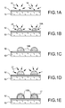
- FIGS. 1A to 1E represent the steps of the process according to the invention.
- the purpose of the germination step is to create on the dielectric "seeds" around which the nanocrystals will grow. Since the deposition is done on a dielectric, one must use a precursor capable of depositing on this dielectric. For example, for a silicon oxide dielectric, SiH 4 silane can be used.
- a deposition time is chosen. short enough not to obtain a seed size greater than 1 nm and sufficient to obtain the desired density (knowing that the density of seeds will be equivalent to the density of nanocrystals, since the nanocrystals grow on the seeds). For example, it is possible to choose a deposition time ranging from a few seconds to a few minutes, for example from 10 seconds to 10 minutes.
- a deposition temperature sufficient for the precursor gas to dissociate is also chosen. If it is desired to obtain crystalline seeds, the deposition temperature must be sufficient to obtain a crystalline and non-amorphous deposit. It should be noted that the time and the deposition temperature are difficult to dissociate and the choice of one influences the choice of the other.
- the temperature may be between 550 and 650 ° C, for example 600 ° C.
- a relatively high partial pressure of the precursor gas of the seeds is chosen, that is to say a pressure of between 10 mTorr and 1 Torr, so as to obtain a high density of seeds.
- the partial pressure may for example be 60 mTorr.
- the growth stage makes it possible to grow the nanocrystals from the seeds to the desired size, without creating new nanocrystals.
- the precursor gas of the nanocrystals is chosen so that it dissociates on the existing seeds, but not on the dielectric.
- the size of the nanocrystals is limited by so-called coalescence (the point where the islets begin to join to form a continuous layer) and the density of the nanocrystals is therefore set in the previous stage of germination.
- a selective precursor gas and a controlled growth rate are thus chosen to obtain the desired nanocrystal size.
- dichlorosilane (DCS), GeH 4 germane or a mixture of both can be selected as the precursor gas.
- the temperature and the growth time are chosen so as to obtain the desired size of the nanocrystals.
- the partial pressure of the precursor gas (s) of the nanocrystals is also chosen as a function of the size of the nanocrystals and therefore of the desired growth rate.
- a precursor gas of the DCS will be chosen, a temperature generally greater than that of the germination stage (between 600 and 850 ° C for example), a deposition time also greater than that of the germination step (a few minutes) and a partial pressure less than or equal to that of the germination step.
- the passivation step consists of depositing a protective layer on the nanocrystals, so that they do not oxidize.
- the ideal material for forming an effective barrier to oxidation is silicon nitride.
- the passivation layer is located only on the nanocrystals. It is therefore necessary that the deposit is selective, so that the deposit takes place only on the nanocrystals, but not on the dielectric.
- a selective precursor gas s.
- the selective precursor gas may be DCS to which NH 3 ammonia is added to form a mixture.
- the selective precursor gas may be GeH 4 or GeCl 4 to which NH 3 ammonia is added to form a mixture.
- the silicon nitride layer must cover the nanocrystals and be capable of acting as a barrier to oxidation, but must also be sufficiently fine, or have lasted for a short period of time, so that the growth of the silicon nitride not take place on the dielectric.
- a thick nitride is an effective barrier to oxidation because the oxidizing species are blocked by the nitride and only the surface of the nitride layer oxidizes. But below a certain thickness (called critical thickness), the oxidizing species pass through the nitride layer and oxidize the nanocrystal present under the nitride.
- This critical thickness is of the order of a few nanometers and depends on several factors, in particular the temperature and the selectivity of the nitride deposit.
- the critical thickness is 3 nm and is 5 nm for a nitride at 750 ° C. (see document [5] ).
- nitride deposition is frequently referred to in the literature as "nucleation delay” or "incubation period”.
- This incubation period is maximum when depositing nitride on a thermal oxide, it remains significant on silicon with a native oxide on the surface, it decreases if the nitride is deposited on nitride (with an oxidized surface in the air ) and it decreases further if it is deposited on a deoxidized silicon or nitride surface (generally obtained by an HF cleaning).
- nitride deposition conditions there is a delay in the literature of about 8 minutes on a thermal oxide, then about 5 minutes on silicon with native surface oxide, and finally, on silicon with a deoxidized surface or bare silicon, this delay is almost reduced to zero. This is explained by the different surface states, more or less favorable to nucleation.
- a thermal oxide has siloxane -Si-O-Si- bonds at the surface, which represents the most unfavorable case for nucleation, the intermediate case corresponds to a majority of silanol Si-OH bonds for the native oxide and the most favorable case is the Si-H bond on bare silicon.
- a selective nitride deposit is thus obtained if one places oneself under these conditions, the most favorable case being a surface with bare silicon against a thermal oxide, with a deposition time of less than 8 minutes.
- a nitride deposited on oxide or silicon with a native surface oxide had a non-stoichiometric sub-layer, called a transition layer, ranging from 3 to 5 nm depending on the deposition temperature.
- this transition sublayer disappears (or tends to disappear) to leave instead a directly stoichiometric layer.
- a stoichiometric nitride has a very good resistance to oxidation and a thin nitride of 2 nm deposited on deoxidized silicon is a barrier to oxidation sufficiently effective for resist oxidation at 850 ° C, whether the nitride film is deposited at 650 ° C or 750 ° C.
- a silicon nitride of 2 nm thick can be sufficiently effective to protect silicon nanocrystals if the deposit is stoichiometric, that is to say made on bare silicon . It is therefore important that the nitride deposition is a stoichiometric deposit. Regarding the selectivity of the deposit, it is placed in the most favorable conditions, that is to say, bare silicon against thermal oxide and a deposition time of less than 8 minutes.
- the nitride deposition conditions are those of a standard nitride deposit, that is to say that the temperature can be the same as that of the growth step of the nanocrystals (in the range of 600 -850 ° C for example), the partial pressures and the DCS / NH 3 ratio are those of a standard LPCVD nitride deposit. Only the deposition time, which must imperatively be less than 8 minutes to have a selective deposition, and the total pressure, which makes it possible to control the speed of growth and therefore the thickness of deposited nitride (of the order of 2- 3 nm for example), must be adjusted.
- silicon nanocrystals on a thermal oxide dielectric substrate, the nanocrystals being embedded in silicon nitride.
- a thermal oxide layer is formed on a silicon substrate.
- the thermal oxide substrate is placed in the enclosure of a technological frame.
- the enclosure is heated gradually to the germination temperature, according to a temperature ramp under an inert gas atmosphere (nitrogen N 2 or hydrogen H 2 ).
- the substrate is surface cleaned prior to undergoing germination to promote a particular surface condition.
- the thermal oxide substrate can undergo surface chemical cleaning with a HF solution to promote silanol (-OH) terminations, which are preferred nucleation sites for silicon nanocrystals. .
- a precursor gas 11 is sent onto the substrate 13 covered with a dielectric layer 12, which will allow the formation of seeds 14 on the dielectric 12 (FIG. Figure 1A ).
- the silicon seeds 14 may be formed at a temperature of between 550 ° C and 700 ° C and at a silane partial pressure of less than about 133 Pa (1 Torr).
- the deposition temperature range is chosen so that the temperature is high enough that the precursor can dissociate and cause the formation of a seed crystal, and also the lowest possible to limit the growth rate of the seeds. germs.
- the germination step is followed by a selective growth step of silicon nanocrystals on the seeds.
- a precursor gas 21 is sent from the nano-structures 16A that one wishes to obtain, that is to say nano-silicon structures, and these will selectively grow on the seeds 14 formed during the germination stage ( Figure 1B ).
- the nanocrystals will grow until reaching a determined size at the end of the growth step, the size of the nanocrystals being determined by the choice of the temperature and the deposition time of the growth step, as well as by the pressure partial of the precursor gas used: nanocrystals of homogeneous size 16 B are thus obtained ( figure 1C ).
- 60 cc of a dichlorosilane gas DCS is injected at a pressure of 60 mT, gradually increasing the temperature from 600 to 700 ° C for 10 minutes.
- the rise in temperature is of the order of a few seconds to go from 600 ° C to 700 ° C. It is then necessary to add a specific growth step of the nanocrystals with dichlorosilane for a few minutes at 700 ° C.
- the encapsulation of silicon nanocrystals 16B is carried out by injecting a mixture of precursor gases 31 composed of 0.2 slm of NH 3 and 40 cc of DCS, at a pressure of 220 mT, at a temperature of 700 ° C. and for a period of 5 minutes ( figure 1D ).
- a mixture of precursor gases 31 composed of 0.2 slm of NH 3 and 40 cc of DCS, at a pressure of 220 mT, at a temperature of 700 ° C. and for a period of 5 minutes ( figure 1D ).
- the temperature in the chamber is lowered to ambient temperature, according to a temperature ramp under an inert nitrogen gas.
- a device consisting of a substrate 13 comprising a thermal oxide layer 12 and silicon nanocrystals 16B coated with silicon nitride 17 is thus obtained.
- the nanocrystals have a silicon core which measures between 6 and 8 nm.
- the silicon nitride layer has a thickness of approximately 2 nm.
- the density of nanocrystals is about 10 12 nanocrystals per cm 2 .
- the gases used during the process for producing the silicon nanocrystals on the dielectric substrate in thermal oxide are sent into the enclosure in a continuous flow: there is thus a continuous flow of different successive gases within a same speaker during the process.
- nanocrystals on a dielectric and protected by a nitride layer may be useful for making flash memories.
- silicon nanocrystals are produced on a silicon oxide dielectric and the nanocrystals are covered with silicon nitride.
- the other steps of formation of the flash memories are similar to the conventional formation steps.
Landscapes
- Chemical & Material Sciences (AREA)
- Engineering & Computer Science (AREA)
- Nanotechnology (AREA)
- General Chemical & Material Sciences (AREA)
- Chemical Kinetics & Catalysis (AREA)
- Materials Engineering (AREA)
- Mechanical Engineering (AREA)
- Metallurgy (AREA)
- Organic Chemistry (AREA)
- Inorganic Chemistry (AREA)
- Mathematical Physics (AREA)
- Theoretical Computer Science (AREA)
- Crystallography & Structural Chemistry (AREA)
- Physics & Mathematics (AREA)
- Non-Volatile Memory (AREA)
- Semiconductor Memories (AREA)
- Formation Of Insulating Films (AREA)
Applications Claiming Priority (1)
| Application Number | Priority Date | Filing Date | Title |
|---|---|---|---|
| FR0655561A FR2910176B1 (fr) | 2006-12-15 | 2006-12-15 | Procede de realisation d'un dispositif a base de nanocristaux recouverts d'une couche de nitrure deposee par cvd |
Publications (2)
| Publication Number | Publication Date |
|---|---|
| EP1933373A2 true EP1933373A2 (de) | 2008-06-18 |
| EP1933373A3 EP1933373A3 (de) | 2009-07-08 |
Family
ID=38283617
Family Applications (1)
| Application Number | Title | Priority Date | Filing Date |
|---|---|---|---|
| EP07122702A Ceased EP1933373A3 (de) | 2006-12-15 | 2007-12-10 | Verfahren zur Herstellung einer Vorrichtung auf der Grundlage von Nanokristallen, die mit einer Nitridschicht beschichtet sind, die durch chemische Dampfabscheidung (CVD) aufgebracht wurde |
Country Status (3)
| Country | Link |
|---|---|
| US (2) | US20080203460A1 (de) |
| EP (1) | EP1933373A3 (de) |
| FR (1) | FR2910176B1 (de) |
Families Citing this family (4)
| Publication number | Priority date | Publication date | Assignee | Title |
|---|---|---|---|---|
| US20090246510A1 (en) * | 2008-03-25 | 2009-10-01 | Commissariat A L'energie Atomique | Metallic nanocrystal patterning |
| US20090243048A1 (en) * | 2008-03-25 | 2009-10-01 | Joel Dufourcq | Metallic nanocrystal encapsulation |
| EP2194055B1 (de) | 2008-12-03 | 2012-04-04 | Novaled AG | Verbrückte Pyridochinazolin- oder Phenathronlin-Verbindungen und organisches Halbleitermaterial mit dieser Verbindung |
| KR20200021030A (ko) * | 2018-08-17 | 2020-02-27 | 삼성디스플레이 주식회사 | 반도체 소자의 제조 방법 및 그를 이용한 반도체 소자 |
Family Cites Families (6)
| Publication number | Priority date | Publication date | Assignee | Title |
|---|---|---|---|---|
| JP2687758B2 (ja) * | 1991-05-27 | 1997-12-08 | 日本電気株式会社 | 半導体装置の製造方法 |
| US6297095B1 (en) * | 2000-06-16 | 2001-10-02 | Motorola, Inc. | Memory device that includes passivated nanoclusters and method for manufacture |
| FR2847567B1 (fr) * | 2002-11-22 | 2005-07-01 | Commissariat Energie Atomique | Procede de realisation par cvd de nano-structures de materiau semi-conducteur sur dielectrique, de tailles homogenes et controlees |
| US20050258467A1 (en) * | 2004-05-21 | 2005-11-24 | Taiwan Semiconductor Manufacturing Co., Ltd. | Nano-crystal non-volatile memory device employing oxidation inhibiting and charge storage enhancing layer |
| US7091130B1 (en) * | 2004-06-25 | 2006-08-15 | Freescale Semiconductor, Inc. | Method of forming a nanocluster charge storage device |
| US7626864B2 (en) * | 2006-04-26 | 2009-12-01 | Chih-Hsin Wang | Electrically alterable non-volatile memory cells and arrays |
-
2006
- 2006-12-15 FR FR0655561A patent/FR2910176B1/fr not_active Expired - Fee Related
-
2007
- 2007-12-10 EP EP07122702A patent/EP1933373A3/de not_active Ceased
- 2007-12-14 US US11/956,902 patent/US20080203460A1/en not_active Abandoned
-
2009
- 2009-09-30 US US12/570,869 patent/US8338276B2/en not_active Expired - Fee Related
Non-Patent Citations (5)
| Title |
|---|
| B. DE SALVO ET AL.: "How far will Silicon Nanocrystals push the scaling limits of NVMs technologies?", TECHNICAL DIGEST OF IEEE INTERNATIONAL ELECTRON DEVICES MEETING 2003, 7 December 2003 (2003-12-07), pages 597 - 600, XP010684082 |
| F. MAZEN ET AL.: "A two step process for the growth of silicon nano-crystals", APPLIED SURFACE SCIENCE, vol. 214, March 2003 (2003-03-01), pages 359 - 363, XP002248266, DOI: doi:10.1016/S0169-4332(03)00521-X |
| K. C. SCHEER ET AL.: "Thermal oxidation of silicon nanocrystals in 0 and NO ambient", JOURNAL OF APPLIED PHYSICS, vol. 93, no. 9, 1 May 2003 (2003-05-01), XP012059582, DOI: doi:10.1063/1.1565172 |
| M YOSHIMARU ET AL.: "Effets of Deposition Temperature on the Oxidation Resistance and Electrical Characteristics of Silicon Nitride", IEEE TRANSACTIONS ON ELECTRON DEVICES, vol. 41, no. 10, October 1994 (1994-10-01), XP000469646, DOI: doi:10.1109/16.324583 |
| S HUANG ET AL.: "Toward Long-Term Retention-Time Single-Electron-Memory Devices Based on Nitrided Nanocrystalline Silicon Dots", IEEE TRANSACTIONS ON NANOTECHNOLOGY, vol. 3, no. 1, March 2004 (2004-03-01), XP001190673, DOI: doi:10.1109/TNANO.2004.824037 |
Also Published As
| Publication number | Publication date |
|---|---|
| US20080203460A1 (en) | 2008-08-28 |
| US8338276B2 (en) | 2012-12-25 |
| FR2910176A1 (fr) | 2008-06-20 |
| FR2910176B1 (fr) | 2009-10-23 |
| US20100035415A1 (en) | 2010-02-11 |
| EP1933373A3 (de) | 2009-07-08 |
Similar Documents
| Publication | Publication Date | Title |
|---|---|---|
| EP1837916B1 (de) | Verfahren zum Herstellen eines Transistors mit einem Germanium enthaltenden Kanal | |
| US6348380B1 (en) | Use of dilute steam ambient for improvement of flash devices | |
| TWI436455B (zh) | 半導體-氧化物-氮化物-氧化物-半導體(sonos)氧化物-氮化物-氧化物(ono)堆疊縮放 | |
| CN101558481B (zh) | 制造非易失性电荷俘获存储器件的基团氧化制程 | |
| EP0887843B1 (de) | Verfahren zur Herstellung eines Transistors mit einem Silizium-Germanium-Gatter | |
| TWI604595B (zh) | 非揮發性電荷捕獲記憶體元件以及其製造方法 | |
| CN101548385A (zh) | 非易失性电荷俘获存储器件的单晶硅制造工艺 | |
| FR2919427A1 (fr) | Structure a reservoir de charges. | |
| FR2847567A1 (fr) | Procede de realisation par cvd de nano-structures de materiau semi-conducteur sur dielectrique, de tailles homogenes et controlees | |
| EP1333473A1 (de) | Interpoly-Dielektrikum-Herstellungsverfahren für Festwerthalbleiterspeicher | |
| JP2002217317A (ja) | 不揮発性半導体記憶装置およびその製造方法 | |
| EP1933373A2 (de) | Verfahren zur Herstellung einer Vorrichtung auf der Grundlage von Nanokristallen, die mit einer Nitridschicht beschichtet sind, die durch chemische Dampfabscheidung (CVD) aufgebracht wurde | |
| US6984562B2 (en) | Method for forming dielectric layer between gates in flash memory device | |
| EP3246948B1 (de) | Verfahren zur herstellung von transistoren, die unterschiedliche eigenschaften aufweisen, auf demselben substrat | |
| WO2011114046A1 (fr) | Procédé de réalisation d'une électrode conductrice | |
| KR100636022B1 (ko) | 반도체 장치의 박막 형성 방법 및 이를 이용한 불휘발성메모리 장치의 제조 방법. | |
| EP1166362A1 (de) | Neues halbleiterbauelement, das die vorteile der massen- und soi-architektur kombiniert, und dessen herstellungsverfahren | |
| TWI709174B (zh) | 用於製造非揮發性電荷捕獲記憶體元件之基氧化方法 | |
| KR100695161B1 (ko) | Ge 나노 클러스터 제조방법 | |
| FR2767965A1 (fr) | Procede de fabrication d'un dispositif a circuit integre ayant differentes epaisseurs d'oxyde de grille | |
| FR3125916A1 (fr) | Procede de realisation de portions dielectriques laterales | |
| CN115249655A (zh) | 半导体结构的制备方法 | |
| JP2009111227A (ja) | 半導体装置の製造方法および不揮発性半導体メモリ | |
| US6319857B1 (en) | Method of fabricating stacked N-O-N ultrathin gate dielectric structures | |
| KR100745604B1 (ko) | 반도체 소자 및 그 형성 방법 |
Legal Events
| Date | Code | Title | Description |
|---|---|---|---|
| PUAI | Public reference made under article 153(3) epc to a published international application that has entered the european phase |
Free format text: ORIGINAL CODE: 0009012 |
|
| AK | Designated contracting states |
Kind code of ref document: A2 Designated state(s): AT BE BG CH CY CZ DE DK EE ES FI FR GB GR HU IE IS IT LI LT LU LV MC MT NL PL PT RO SE SI SK TR |
|
| AX | Request for extension of the european patent |
Extension state: AL BA HR MK RS |
|
| PUAL | Search report despatched |
Free format text: ORIGINAL CODE: 0009013 |
|
| AK | Designated contracting states |
Kind code of ref document: A3 Designated state(s): AT BE BG CH CY CZ DE DK EE ES FI FR GB GR HU IE IS IT LI LT LU LV MC MT NL PL PT RO SE SI SK TR |
|
| AX | Request for extension of the european patent |
Extension state: AL BA HR MK RS |
|
| 17P | Request for examination filed |
Effective date: 20100107 |
|
| 17Q | First examination report despatched |
Effective date: 20100209 |
|
| AKX | Designation fees paid |
Designated state(s): AT BE BG CH CY CZ DE DK EE ES FI FR GB GR HU IE IS IT LI LT LU LV MC MT NL PL PT RO SE SI SK TR |
|
| RAP1 | Party data changed (applicant data changed or rights of an application transferred) |
Owner name: COMMISSARIAT A L'ENERGIE ATOMIQUE ET AUX ENERGIES |
|
| STAA | Information on the status of an ep patent application or granted ep patent |
Free format text: STATUS: THE APPLICATION HAS BEEN REFUSED |
|
| 18R | Application refused |
Effective date: 20130618 |