EP1936432A2 - Abstandhalter und Flüssigkristallanzeigevorrichtung damit - Google Patents
Abstandhalter und Flüssigkristallanzeigevorrichtung damit Download PDFInfo
- Publication number
- EP1936432A2 EP1936432A2 EP07024593A EP07024593A EP1936432A2 EP 1936432 A2 EP1936432 A2 EP 1936432A2 EP 07024593 A EP07024593 A EP 07024593A EP 07024593 A EP07024593 A EP 07024593A EP 1936432 A2 EP1936432 A2 EP 1936432A2
- Authority
- EP
- European Patent Office
- Prior art keywords
- spacer
- substrate
- layer
- dendrimer
- liquid crystal
- Prior art date
- Legal status (The legal status is an assumption and is not a legal conclusion. Google has not performed a legal analysis and makes no representation as to the accuracy of the status listed.)
- Granted
Links
Images


Classifications
-
- G—PHYSICS
- G02—OPTICS
- G02F—OPTICAL DEVICES OR ARRANGEMENTS FOR THE CONTROL OF LIGHT BY MODIFICATION OF THE OPTICAL PROPERTIES OF THE MEDIA OF THE ELEMENTS INVOLVED THEREIN; NON-LINEAR OPTICS; FREQUENCY-CHANGING OF LIGHT; OPTICAL LOGIC ELEMENTS; OPTICAL ANALOGUE/DIGITAL CONVERTERS
- G02F1/00—Devices or arrangements for the control of the intensity, colour, phase, polarisation or direction of light arriving from an independent light source, e.g. switching, gating or modulating; Non-linear optics
- G02F1/01—Devices or arrangements for the control of the intensity, colour, phase, polarisation or direction of light arriving from an independent light source, e.g. switching, gating or modulating; Non-linear optics for the control of the intensity, phase, polarisation or colour
- G02F1/13—Devices or arrangements for the control of the intensity, colour, phase, polarisation or direction of light arriving from an independent light source, e.g. switching, gating or modulating; Non-linear optics for the control of the intensity, phase, polarisation or colour based on liquid crystals, e.g. single liquid crystal display cells
- G02F1/133—Constructional arrangements; Operation of liquid crystal cells; Circuit arrangements
- G02F1/1333—Constructional arrangements; Manufacturing methods
- G02F1/1339—Gaskets; Spacers; Sealing of cells
- G02F1/13392—Gaskets; Spacers; Sealing of cells spacers dispersed on the cell substrate, e.g. spherical particles, microfibres
Definitions
- the present invention relates to a spacer and a liquid crystal display device having the same. More particularly, the present invention relates to a spacer and a liquid crystal display device including the same, where the spacer has improved adhesion for maintaining a cell gap between two substrates to prevent light leakage from the liquid crystal display device.
- a liquid crystal display (LCD) device includes a first substrate, a second substrate facing the first substrate, and a liquid crystal layer disposed between them.
- An optical characteristic of the LCD device is closely related to a cell gap between the two substrates. Particularly, optical characteristics such as contrast ratio or viewing angle of the LCD device are known to be dependent on a value of a birefringence ( ⁇ n) of liquid crystal multiplied with the cell gap. Thus, if the cell gap of the LCD device is not uniform, the optical characteristic will also not be uniform.
- a spacer of spherical shape which may be called a beads spacer is prevalently used to maintain the cell gap between the two substrates.
- the spacer maintains the cell gap by contacting alignment layers formed on the surfaces of both substrates.
- the present invention provides a spacer having improved adhesion.
- the present invention also provides a LCD device including a spacer having improved adhesion.
- a spacer comprises: a spacer main body; and a coating layer encompassing the spacer main body and comprising a hyper branch polymer.
- the hyper branch polymer comprises a dendrimer.
- the dendrimer comprises: a core part disposed at a central portion of the dendrimer; a terminal part comprising an aliphatic group compound; and a linking part connecting the core part with the terminal part.
- the dendrimer comprises: a core part disposed at a central portion of the dendrimer; a terminal part comprising an aromatic group compound; and a linking part connecting the core part with the terminal part.
- the spacer main body comprises polystyrene.
- the spacer main body comprises an acrylic resin layer in contact with the coating layer.
- the spacer has a spherical shape.
- a liquid crystal display (LCD) device comprises: a first substrate; a second substrate facing the first substrate; a liquid crystal layer disposed between the first substrate and the second substrate; and a spacer maintaining a gap between the first substrate and the second substrate, wherein the spacer comprises: a spacer main body; and a coating layer encompassing the spacer main body and comprising a hyper branch polymer.
- the hyper branch polymer comprises a dendrimer.
- the first substrate comprises a first alignment layer
- the second substrate comprises a second alignment layer
- the coating layer contacts at least one of the first alignment layer and the second alignment layer.
- the first substrate further comprises a pixel electrode formed with a pixel electrode cut-off pattern therein;
- the second substrate further comprises a common electrode formed with a common electrode cut-off pattern therein;
- the liquid crystal layer adopts a vertical align (VA) mode;
- the dendrimer comprises a core part, a branch type linking part, and a terminal part, wherein the terminal part comprises an aliphatic group compound.
- the liquid crystal layer adopts a twisted nematic (TN) mode
- the dendrimer comprises a core part, a branch type linking part, and a terminal part, wherein the terminal part comprises an aromatic group compound.
- the spacer has a spherical shape.
- the spacer main body comprises polystyrene.
- the spacer main body comprises an acrylic resin layer in contact with the coating layer.
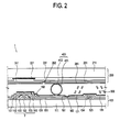
- a LCD device according to a first exemplary embodiment of the present invention is explained referring to FIG. 1 and FIG. 2 .
- the LCD device 1 includes a first substrate 100 with a thin film transistor 'T' formed thereon, a second substrate 200 facing the first substrate 100, a liquid crystal layer 300 disposed between the two substrates 100 and 200, a spacer 400 for maintaining a cell gap, and a sealant (reference numeral 500 in FIG. 5D ).
- the first substrate 100 is explained.
- a gate wire is formed on a first insulating substrate 111.
- the gate wire may be a single metallic layer or multiple metallic layers.
- the gate wire includes a gate line 121 disposed in a display region and extending transversely, a gate electrode 122 connected to the gate line 121, and a storage electrode line 123 extending parallel to the gate line 121.
- a gate insulating layer 131 which may include silicon nitride (SiNx), etc. is formed on the first insulating substrate 111 to cover the gate wire.
- a semiconductor layer 132 including a semiconductor material such as amorphous silicon, etc. is formed on a gate electrode 122 with the gate insulating layer 131 disposed therebetween.
- An ohmic contact layer 133 including silicide or an n+ hydrogenised amorphous silicon highly doped with a n-type impurity is formed on the semiconductor layer 132.
- the ohmic contact layer 133 is eliminated on a channel portion of the semiconductor layer 132 disposed between a source electrode 142 and a drain electrode 143.
- a data wire is formed on the ohmic contact layer 133 and the gate insulating layer 131.
- the data wire may also be a single metallic layer or multiple metallic layers.
- the data wire includes a data line 141 formed longitudinally to cross the gate line 121 and define a pixel, a source electrode 142 branching from the data line 141 and partly extending onto the ohmic contact layer 133, and a drain electrode 143 separated from the source electrode 142 and partly formed on the opposite side of the ohmic contact layer 133.
- a passivation layer 151 is formed on the data wire and the semiconductor layer 132 which is not covered by the data wire.
- a contact hole 152 exposing the drain electrode 143 is formed in the passivation layer 151.
- a pixel electrode 161 is formed on the passivation layer 151.
- the pixel electrode 161 includes a transparent conductive material such as indium tin oxide (ITO) and indium zinc oxide (IZO).
- ITO indium tin oxide
- IZO indium zinc oxide
- the pixel electrode 161 is connected to the drain electrode 143 through the contact hole 152.
- a pixel electrode cut-off pattern 162 is formed in the pixel electrode 161.
- the pixel electrode cut-off pattern 162 and a common electrode cut-off pattern 252 described below divide the liquid crystal layer into a plurality of regions.
- a first alignment layer 171 is formed on the pixel electrode 161, and the passivation layer 151.
- the first alignment layer 171 may include polyimide.
- the second substrate 200 is explained below.
- a black matrix 211 is formed on a second insulating substrate 211.
- the black matrix 221 blocks a direct illumination of a light to the thin film transistor T disposed on the first substrate 100.
- the black matrix 221 includes a photosensitive organic material combined with a black pigment. Carbon black, titanium oxide etc. may be used for the black pigment.
- a color filter 231 including a red, a green, and a blue filter is formed on the substrate 200 with the black matrix 221 as a boundary.
- the color filter 231 assigns color to the light illuminated from a backlight unit (not shown) and transmitted to the liquid crystal layer 300.
- the color filter 231 may include a photosensitive organic material.
- An overcoat layer 241 is formed on the color filter 231 and on the black matrix 221 which is not covered by the color filter 231.
- the overcoat layer 241 provides a planar surface and protects the color filter 231.
- the overcoat layer 241 may include a photosensitive acrylic resin.
- a common electrode 251 is formed on the overcoat layer 241.
- the common electrode 251 includes a transparent conductive material such as ITO or IZO.
- the common electrode 251 and the pixel electrode 161 directly apply a voltage to the liquid crystal layer 300.
- the common electrode cut-off pattern 252 is formed in the common electrode 251. As previously mentioned, the common electrode cut-off pattern 252 and the pixel electrode cut-off pattern 162 divide the liquid crystal layer 300 into a plurality of regions.
- the pixel electrode cut-off pattern 162 and the common electrode cut-off pattern 252 may be formed in various shapes.
- the liquid crystal layer 300 may be divided into a plurality of regions by protruding parts instead of the pixel electrode cut-off pattern 162 and the common electrode cut-off pattern 252 described in the other embodiments.
- a second alignment layer 261 is formed on the common electrode 251.
- the second alignment layer 261 may include polyimide.
- the liquid crystal layer 300 is disposed between the first substrate 100 and the second substrate 200.
- the liquid crystal layer 300 adopts a vertically aligned (VA) mode where liquid crystal molecules are arranged so that their lengthwise direction is vertical when no voltage is applied. When the voltage is applied, the liquid crystal molecules of negative anisotropic dielectric constant are arranged perpendicular to an applied electric field.
- VA vertically aligned
- the liquid crystal molecules without a determined azimuth angle are randomly arranged in various directions and produce a disclination line at a boundary made by the different orientation directions.
- the pixel electrode cut-off pattern 162 and the common electrode cut-off pattern 252 make a fringe field and determine the liquid crystal molecules' azimuth angle when the voltage is applied to the liquid crystal layer 300.
- the liquid crystal layer 300 is divided into multiple regions according to an arrangement of the pixel electrode cut-off pattern 162 and the common electrode cut-off pattern 252.
- the spacer 400 maintains a cell gap between the first substrate 100 and the second substrate 200 by contacting the first alignment layer 171 and/or the second alignment layer 261.
- the spacer 400 has a spherical shape and includes a spacer main body 411 and a coating layer 412 encompassing the spacer main body 411.
- the spacer main body 411 may include a resin such as polystyrene.
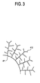
- the coating layer 412 includes a hyper branch polymer.
- the hyper branch polymer is formed by a coupling of monomers having at least three functional groups.
- the hyper branch polymer different from a linear polymer, has a plurality of branches extending from a main polymer chain and includes a dendrimer.
- the hyper branch polymer also includes a compound which has dendrimer structure but has a structural defect to have uncomplete three-dimensional tree branch structure.
- the dendrimer denotes a giant mono molecule arranged in a three-dimensional tree branch structure.
- the dendrimer is quite different from a typical linear polymer in structure and physical characteristics because the dendrimer has an aligned symmetrical structure with high order.
- the dendrimer as exemplarily illustrated below, includes a core part, a linking part, and a terminal part.
- the core part is disposed at a center portion of the dendrimer.
- a plurality of linking parts extending from the core part are formed in multiple generations. Though a structure of three generations is illustrated in the formula below, the structure is not limited thereto but may be varied by adjusting a molecular weight with a number of the generation.
- the terminal part disposed at an end portion of the linking part determines a solubility, surface characteristic, etc.
- the terminal part may include a functional group.
- the spacer 400 has an excellent adhesion to the first substrate 100 and the second substrate 200 to prevent the alignment layers 171 and 261 from being damaged by vibration or impact to the LCD device.
- FIG. 3 illustrates the spacer 400 including the coating layer 412 of a hyper branch polymer which is not a dendrimer
- FIG. 4 illustrates the spacer 400 including the coating layer 412 of a dendrimer.
- an end portion of the polymer is exposed.
- the exposed end portion of the polymer enhances the adhesion of the interaction between the spacer and the first alignment layer 171 and/or the second alignment layer 261.
- the coating layer 412 does not include the hyper branch linear polymer, the end portion of the polymer may not be exposed at the surface because the polymer chains are interacting within the coating layer 412. Accordingly, the interaction of the spacer with the first alignment layer 171 and/or the second alignment layer 261 may be limited, degrading the adhesion of the spacer 400.
- the terminal part (O) it is desirable for the terminal part (O) to include an aliphatic group compound if the dendrimer is used for the coating layer 412.
- the aliphatice group of the dendrimer may have five or more carbons.
- an acrylic group, an amine group, an ester group, a carboxyl group, an aldehyde group, a hydroxy group and an ethylene oxide group, or other functional groups may be provided for the terminal part of the dendrimer.
- the surface of the spacer main body 411 may include an acrylic resin coating layer, where the coating layer 412 directly contacts the acrylic resin coating layer.
- the first alignment layer 171 and/or the second alignment layer 261 may not be formed depending on a mode of the liquid crystal layer 300.
- the spacer 400 may contact the pixel electrode 161, the common electrode 251, and/or the insulating layer rather than the first alignment layer 171 and/or the second alignment layer 261. Even if the spacer 400 contacts a layer other than the first alignment layer 171 and/or the second alignment layer 261, the coating layer 412 may still enhance the adhesion of the spacer 400.
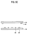
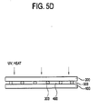
- FIG. 5A , FIG. 5B , FIG. 5C , and FIG. 5D A manufacturing method of the LCD device 1 according to the first exemplary embodiment referring to FIG. 5A , FIG. 5B , FIG. 5C , and FIG. 5D is explained below. An explanation for a known method of manufacturing the first substrate 100 and the second substrate 200 is omitted.
- a sealant 500 is formed on the second substrate 200.
- the sealant 500 may be formed on the first substrate 100 by a drawing method using a dispenser.
- the sealant 500 may be formed in a rectangular shape.
- the sealant 500 may include epoxy resin and acrylic resin as main ingredients, amine group hardener, a filler such as alumina powder, and a solvent such as propylene-glycol-diacetate.
- the liquid crystal layer 300 is formed on the first substrate 100 by dropping, and the spacer 400 is dispersed.
- the liquid crystal layer 300 does not flow on the first substrate 100 by its own viscosity.
- the spacer 400 is fixed to the first alignment layer 171 on the first substrate 100.
- the second substrate 200 is aligned with the first substrate 100 while disposing the sealant 500 therebetween as shown in FIG. 5C .
- the sealant 500 is cured by an ultra violet ray and/or heat.
- FIG. 6 another manufacturing method for the LCD device according to the first exemplary embodiment is explained.
- the sealant 500 formed on the second substrate 200 is approximately a rectangular shape, the sealant 500 may be open on one side.
- the first substrate 100 and the second substrate 200 are coupled and the liquid crystal layer 300 is formed by injection into the space between the first substrate 100 and the second substrate 200.
- the injection is performed by a filling method in which a vacuous space between the first substrate 100 and the second substrate 200 is filled with the liquid crystals.
- the open side portion is filled with a resin and the resin is cured with an ultra violet ray and/or heat.
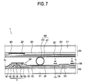
- FIG. 7 An LCD device according to a second exemplary embodiment of the present invention is explained referring to FIG. 7 .
- a cut-off pattern is not formed in a pixel electrode 161 nor in a common electrode 251 and a liquid crystal layer 300 adopts a twisted nematic (TN) mode.
- TN twisted nematic
- aromatic group compounds exist on a surface of a first alignment layer 171 and/or a second alignment layer 261, in the second exemplary embodiment that uses the TN mode liquid crystal layer 300.
- a terminal part (O) of a dendrimer as a coating layer 412 it is preferred, but not necessary for a terminal part (O) of a dendrimer as a coating layer 412 to include an aromatic group compound.
- the present invention provides a spacer having improved adhesion and a liquid crystal display device including the spacer having improved adhesion.
Landscapes
- Physics & Mathematics (AREA)
- Nonlinear Science (AREA)
- Mathematical Physics (AREA)
- Chemical & Material Sciences (AREA)
- Crystallography & Structural Chemistry (AREA)
- General Physics & Mathematics (AREA)
- Optics & Photonics (AREA)
- Liquid Crystal (AREA)
Applications Claiming Priority (1)
| Application Number | Priority Date | Filing Date | Title |
|---|---|---|---|
| KR1020060131912A KR101349095B1 (ko) | 2006-12-21 | 2006-12-21 | 스페이서와 이를 포함하는 액정표시장치 |
Publications (3)
| Publication Number | Publication Date |
|---|---|
| EP1936432A2 true EP1936432A2 (de) | 2008-06-25 |
| EP1936432A3 EP1936432A3 (de) | 2008-07-02 |
| EP1936432B1 EP1936432B1 (de) | 2010-03-03 |
Family
ID=39299781
Family Applications (1)
| Application Number | Title | Priority Date | Filing Date |
|---|---|---|---|
| EP07024593A Active EP1936432B1 (de) | 2006-12-21 | 2007-12-19 | Abstandhalter und Flüssigkristallanzeigevorrichtung damit |
Country Status (6)
| Country | Link |
|---|---|
| US (1) | US8085380B2 (de) |
| EP (1) | EP1936432B1 (de) |
| JP (1) | JP5305625B2 (de) |
| KR (1) | KR101349095B1 (de) |
| CN (1) | CN101206351B (de) |
| DE (1) | DE602007005082D1 (de) |
Families Citing this family (4)
| Publication number | Priority date | Publication date | Assignee | Title |
|---|---|---|---|---|
| CN102967958B (zh) * | 2012-10-17 | 2016-11-09 | 张素玲 | 具间隔微结构的液晶薄膜及其制造方法 |
| CN105295765B (zh) * | 2015-10-12 | 2018-07-17 | 京东方科技集团股份有限公司 | 一种封框胶的填充物、其制作方法及封框胶 |
| CN205723639U (zh) | 2016-04-19 | 2016-11-23 | 鄂尔多斯市源盛光电有限责任公司 | 一种封框胶结构、显示面板和显示装置 |
| TWI880452B (zh) * | 2023-10-07 | 2025-04-11 | 瑞儀光電股份有限公司 | 背光模組及顯示裝置 |
Family Cites Families (13)
| Publication number | Priority date | Publication date | Assignee | Title |
|---|---|---|---|---|
| JPS5713425A (en) * | 1980-06-27 | 1982-01-23 | Canon Inc | Surface treatment of material for spacer |
| JPH0427917A (ja) | 1990-05-23 | 1992-01-30 | Kao Corp | 液晶表示用スペーサ及びその製造方法 |
| JP2679926B2 (ja) * | 1992-01-29 | 1997-11-19 | 積水フアインケミカル株式会社 | 液晶表示素子用スペーサー、液晶表示素子及びその製造方法 |
| JP4493746B2 (ja) * | 1998-11-30 | 2010-06-30 | 東レ・ダウコーニング株式会社 | コーティング材 |
| JP3947323B2 (ja) | 1999-05-10 | 2007-07-18 | 積水化学工業株式会社 | 液晶表示素子用スペーサ及び液晶表示素子 |
| KR100377946B1 (ko) | 2000-07-15 | 2003-03-29 | 한국과학기술원 | 덴드리머를 이용한 단분자막의 제조방법 |
| JP2002167368A (ja) * | 2000-12-01 | 2002-06-11 | Nitto Denko Corp | アルキル置換デンドリマーおよびその製造法 |
| EP1277770A1 (de) * | 2001-07-17 | 2003-01-22 | Rolic AG | Photoaktive Materialien |
| US6806223B2 (en) | 2002-04-19 | 2004-10-19 | Central Michigan University Board Of Trustees | Single oxygen catalysts including condensed carbon molecules |
| JP2004045922A (ja) * | 2002-07-15 | 2004-02-12 | Fuji Photo Film Co Ltd | 導光部材 |
| JP4277947B2 (ja) * | 2002-07-18 | 2009-06-10 | シャープ株式会社 | デンドリマー及びこれを用いた電子デバイス素子 |
| KR20050057353A (ko) * | 2002-09-19 | 2005-06-16 | 코닌클리즈케 필립스 일렉트로닉스 엔.브이. | 스페이서에 의해 서로 이격된 한 쌍의 기판 및 그것의 제조방법, 그것을 포함하는 장치 및 lcd 기판 |
| KR100568083B1 (ko) | 2003-12-10 | 2006-04-05 | 제일모직주식회사 | 표면 관능화된 단분산성 고분자 미립자, 그 제조 방법, 및그 미립자를 이용한 스페이서 |
-
2006
- 2006-12-21 KR KR1020060131912A patent/KR101349095B1/ko active Active
-
2007
- 2007-09-07 JP JP2007233272A patent/JP5305625B2/ja active Active
- 2007-10-31 US US11/933,304 patent/US8085380B2/en active Active
- 2007-12-11 CN CN200710196826XA patent/CN101206351B/zh active Active
- 2007-12-19 EP EP07024593A patent/EP1936432B1/de active Active
- 2007-12-19 DE DE602007005082T patent/DE602007005082D1/de active Active
Also Published As
| Publication number | Publication date |
|---|---|
| KR101349095B1 (ko) | 2014-01-16 |
| CN101206351B (zh) | 2012-01-11 |
| US20080151173A1 (en) | 2008-06-26 |
| EP1936432B1 (de) | 2010-03-03 |
| JP2008158492A (ja) | 2008-07-10 |
| JP5305625B2 (ja) | 2013-10-02 |
| US8085380B2 (en) | 2011-12-27 |
| KR20080057952A (ko) | 2008-06-25 |
| EP1936432A3 (de) | 2008-07-02 |
| CN101206351A (zh) | 2008-06-25 |
| DE602007005082D1 (de) | 2010-04-15 |
Similar Documents
| Publication | Publication Date | Title |
|---|---|---|
| US7679693B2 (en) | Liquid crystal display device and manufacturing method thereof | |
| US8525964B2 (en) | Array substrate, method of manufacturing the same, display panel having the same, and liquid crystal display apparatus having the same | |
| US7751014B2 (en) | Liquid-crystal display device | |
| US9201258B2 (en) | Display device with image display part in a cavity | |
| US8432521B2 (en) | Liquid crystal display and manufacturing method of the same | |
| US7671942B2 (en) | Transflective LCD device and method having first domain in reflective portion, second and third domains in transmission portion and with additional electrodes in third domain for third storage electrode | |
| CN104749839A (zh) | 弯曲液晶显示器 | |
| US7884912B2 (en) | Liquid crystal display device | |
| US20150268494A1 (en) | Liquid crystal display and manufacturing method thereof | |
| KR20120131783A (ko) | 액정 표시 장치 및 그 제조 방법 | |
| US20170066968A1 (en) | Composition for aligment layer, array substrate for display device comprising the same | |
| US20070296881A1 (en) | Array substrate for liquid crystal display device | |
| EP1936432B1 (de) | Abstandhalter und Flüssigkristallanzeigevorrichtung damit | |
| KR101951304B1 (ko) | 액정 표시 장치 및 그 제조 방법 | |
| US9448438B2 (en) | Liquid crystal display panel comprising alignment molecules having a core portion, a polarity portion, and a tail portion | |
| US9989825B2 (en) | Display device | |
| US9563085B2 (en) | Display device | |
| US9541810B2 (en) | Liquid crystal display device | |
| US7948597B2 (en) | Liquid crystal display panel for liquid crystal display | |
| KR101893892B1 (ko) | 액정 표시 장치 및 그 제조 방법 | |
| KR101536124B1 (ko) | 액정표시장치 및 이의 제조 방법 | |
| US20090201452A1 (en) | Liquid crystal composition and display device having the same | |
| KR20170049753A (ko) | 절연층, 광차단층 및 이를 포함하는 어레이 기판 및 표시장치 | |
| KR20110138965A (ko) | 액정표시장치 | |
| GB2475535A (en) | Display with wire grid polarizer capacitively coupled to driving arrangement |
Legal Events
| Date | Code | Title | Description |
|---|---|---|---|
| PUAI | Public reference made under article 153(3) epc to a published international application that has entered the european phase |
Free format text: ORIGINAL CODE: 0009012 |
|
| PUAL | Search report despatched |
Free format text: ORIGINAL CODE: 0009013 |
|
| AK | Designated contracting states |
Kind code of ref document: A2 Designated state(s): AT BE BG CH CY CZ DE DK EE ES FI FR GB GR HU IE IS IT LI LT LU LV MC MT NL PL PT RO SE SI SK TR |
|
| AX | Request for extension of the european patent |
Extension state: AL BA HR MK RS |
|
| AK | Designated contracting states |
Kind code of ref document: A3 Designated state(s): AT BE BG CH CY CZ DE DK EE ES FI FR GB GR HU IE IS IT LI LT LU LV MC MT NL PL PT RO SE SI SK TR |
|
| AX | Request for extension of the european patent |
Extension state: AL BA HR MK RS |
|
| 17P | Request for examination filed |
Effective date: 20081122 |
|
| 17Q | First examination report despatched |
Effective date: 20090108 |
|
| AKX | Designation fees paid |
Designated state(s): DE FR GB NL |
|
| GRAP | Despatch of communication of intention to grant a patent |
Free format text: ORIGINAL CODE: EPIDOSNIGR1 |
|
| GRAS | Grant fee paid |
Free format text: ORIGINAL CODE: EPIDOSNIGR3 |
|
| GRAA | (expected) grant |
Free format text: ORIGINAL CODE: 0009210 |
|
| AK | Designated contracting states |
Kind code of ref document: B1 Designated state(s): DE FR GB NL |
|
| REG | Reference to a national code |
Ref country code: GB Ref legal event code: FG4D |
|
| REF | Corresponds to: |
Ref document number: 602007005082 Country of ref document: DE Date of ref document: 20100415 Kind code of ref document: P |
|
| REG | Reference to a national code |
Ref country code: DE Ref legal event code: R096 Ref document number: 602007005082 Country of ref document: DE Effective date: 20100415 |
|
| REG | Reference to a national code |
Ref country code: NL Ref legal event code: T3 |
|
| PLBE | No opposition filed within time limit |
Free format text: ORIGINAL CODE: 0009261 |
|
| STAA | Information on the status of an ep patent application or granted ep patent |
Free format text: STATUS: NO OPPOSITION FILED WITHIN TIME LIMIT |
|
| 26N | No opposition filed |
Effective date: 20101206 |
|
| REG | Reference to a national code |
Ref country code: DE Ref legal event code: R097 Ref document number: 602007005082 Country of ref document: DE Effective date: 20101206 |
|
| REG | Reference to a national code |
Ref country code: NL Ref legal event code: SD Effective date: 20121017 |
|
| REG | Reference to a national code |
Ref country code: FR Ref legal event code: TP Owner name: SAMSUNG DISPLAY CO. LTD, KR Effective date: 20130226 |
|
| REG | Reference to a national code |
Ref country code: GB Ref legal event code: 732E Free format text: REGISTERED BETWEEN 20130307 AND 20130313 |
|
| REG | Reference to a national code |
Ref country code: DE Ref legal event code: R082 Ref document number: 602007005082 Country of ref document: DE Representative=s name: DR. WEITZEL & PARTNER, DE |
|
| REG | Reference to a national code |
Ref country code: DE Ref legal event code: R082 Ref document number: 602007005082 Country of ref document: DE Representative=s name: DR. WEITZEL & PARTNER, DE Effective date: 20130422 Ref country code: DE Ref legal event code: R081 Ref document number: 602007005082 Country of ref document: DE Owner name: SAMSUNG DISPLAY CO., LTD., KR Free format text: FORMER OWNER: SAMSUNG ELECTRONICS CO., LTD., SUWON-SI, KR Effective date: 20130422 Ref country code: DE Ref legal event code: R081 Ref document number: 602007005082 Country of ref document: DE Owner name: SAMSUNG DISPLAY CO., LTD., YONGIN-CITY, KR Free format text: FORMER OWNER: SAMSUNG ELECTRONICS CO., LTD., SUWON-SI, GYEONGGI-DO, KR Effective date: 20130422 Ref country code: DE Ref legal event code: R082 Ref document number: 602007005082 Country of ref document: DE Representative=s name: DR. WEITZEL & PARTNER PATENT- UND RECHTSANWAEL, DE Effective date: 20130422 |
|
| REG | Reference to a national code |
Ref country code: FR Ref legal event code: PLFP Year of fee payment: 9 |
|
| REG | Reference to a national code |
Ref country code: FR Ref legal event code: PLFP Year of fee payment: 10 |
|
| REG | Reference to a national code |
Ref country code: FR Ref legal event code: PLFP Year of fee payment: 11 |
|
| P01 | Opt-out of the competence of the unified patent court (upc) registered |
Effective date: 20230516 |
|
| PGFP | Annual fee paid to national office [announced via postgrant information from national office to epo] |
Ref country code: NL Payment date: 20251120 Year of fee payment: 19 |
|
| PGFP | Annual fee paid to national office [announced via postgrant information from national office to epo] |
Ref country code: DE Payment date: 20251120 Year of fee payment: 19 |
|
| PGFP | Annual fee paid to national office [announced via postgrant information from national office to epo] |
Ref country code: GB Payment date: 20251120 Year of fee payment: 19 |
|
| PGFP | Annual fee paid to national office [announced via postgrant information from national office to epo] |
Ref country code: FR Payment date: 20251125 Year of fee payment: 19 |