EP1936432B1 - Abstandhalter und Flüssigkristallanzeigevorrichtung damit - Google Patents
Abstandhalter und Flüssigkristallanzeigevorrichtung damit Download PDFInfo
- Publication number
- EP1936432B1 EP1936432B1 EP07024593A EP07024593A EP1936432B1 EP 1936432 B1 EP1936432 B1 EP 1936432B1 EP 07024593 A EP07024593 A EP 07024593A EP 07024593 A EP07024593 A EP 07024593A EP 1936432 B1 EP1936432 B1 EP 1936432B1
- Authority
- EP
- European Patent Office
- Prior art keywords
- spacer
- substrate
- layer
- liquid crystal
- dendrimer
- Prior art date
- Legal status (The legal status is an assumption and is not a legal conclusion. Google has not performed a legal analysis and makes no representation as to the accuracy of the status listed.)
- Active
Links
Images


Classifications
-
- G—PHYSICS
- G02—OPTICS
- G02F—OPTICAL DEVICES OR ARRANGEMENTS FOR THE CONTROL OF LIGHT BY MODIFICATION OF THE OPTICAL PROPERTIES OF THE MEDIA OF THE ELEMENTS INVOLVED THEREIN; NON-LINEAR OPTICS; FREQUENCY-CHANGING OF LIGHT; OPTICAL LOGIC ELEMENTS; OPTICAL ANALOGUE/DIGITAL CONVERTERS
- G02F1/00—Devices or arrangements for the control of the intensity, colour, phase, polarisation or direction of light arriving from an independent light source, e.g. switching, gating or modulating; Non-linear optics
- G02F1/01—Devices or arrangements for the control of the intensity, colour, phase, polarisation or direction of light arriving from an independent light source, e.g. switching, gating or modulating; Non-linear optics for the control of the intensity, phase, polarisation or colour
- G02F1/13—Devices or arrangements for the control of the intensity, colour, phase, polarisation or direction of light arriving from an independent light source, e.g. switching, gating or modulating; Non-linear optics for the control of the intensity, phase, polarisation or colour based on liquid crystals, e.g. single liquid crystal display cells
- G02F1/133—Constructional arrangements; Operation of liquid crystal cells; Circuit arrangements
- G02F1/1333—Constructional arrangements; Manufacturing methods
- G02F1/1339—Gaskets; Spacers; Sealing of cells
- G02F1/13392—Gaskets; Spacers; Sealing of cells spacers dispersed on the cell substrate, e.g. spherical particles, microfibres
Definitions
- the present invention relates to a spacer and a liquid crystal display device having the same. More particularly, the present invention relates to a spacer and a liquid crystal display device including the same, where the spacer has improved adhesion for maintaining a cell gap between two substrates to prevent light leakage from the liquid crystal display device.
- the spacer main body comprises polystyrene.
- the first substrate further comprises a pixel electrode formed with a pixel electrode cut-off pattern therein;
- the second substrate further comprises a common electrode formed with a common electrode cut-off pattern therein;
- the liquid crystal layer adopts a vertical align (VA) mode;
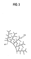
- the dendrimer comprises a core part, a branch type linking part, and a terminal part, wherein the terminal part comprises an aliphatic group compound.
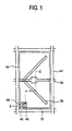
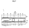
- a gate wire is formed on a first insulating substrate 111.
- the gate wire may be a single metallic layer or multiple metallic layers.
- the gate wire includes a gate line 121 disposed in a display region and extending transversely, a gate electrode 122 connected to the gate line 121, and a storage electrode line 123 extending parallel to the gate line 121.
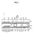
- a color filter 231 including a red, a green, and a blue filter is formed on the substrate 200 with the black matrix 221 as a boundary.
- the color filter 231 assigns color to the light illuminated from a backlight unit (not shown) and transmitted to the liquid crystal layer 300.
- the color filter 231 may include a photosensitive organic material.
- an end portion of the polymer is exposed.
- the exposed end portion of the polymer enhances the adhesion of the interaction between the spacer and the first alignment layer 171 and/or the second alignment layer 261.
- the coating layer 412 does not include the hyper branch linear polymer, the end portion of the polymer may not be exposed at the surface because the polymer chains are interacting within the coating layer 412. Accordingly, the interaction of the spacer with the first alignment layer 171 and/or the second alignment layer 261 may be limited, degrading the adhesion of the spacer 400.
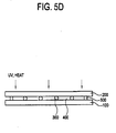
- the sealant 500 is cured by an ultra violet ray and/or heat.
- the first substrate 100 and the second substrate 200 are coupled and the liquid crystal layer 300 is formed by injection into the space between the first substrate 100 and the second substrate 200.
- the injection is performed by a filling method in which a vacuous space between the first substrate 100 and the second substrate 200 is filled with the liquid crystals.
Landscapes
- Physics & Mathematics (AREA)
- Nonlinear Science (AREA)
- Mathematical Physics (AREA)
- Chemical & Material Sciences (AREA)
- Crystallography & Structural Chemistry (AREA)
- General Physics & Mathematics (AREA)
- Optics & Photonics (AREA)
- Liquid Crystal (AREA)
Claims (10)
- Abstandhalter (400), der Folgendes umfasst:einen Abstandhalter-Hauptkörper (411); undeine Beschichtung (412), die den Abstandhalter-Hauptkörper (411) abdeckt und ein hochverzweigtes Polymer umfasst, dadurch gekennzeichnet, dass das hochverzweigte Polymer ein Dendrimer umfasst.
- Abstandhalter (400) gemäß Anspruch 1, wobei das Dendrimer umfasst:einen Kernteil, der in einem Mittelabschnitt des Dendrimers angeordnet ist;einen Terminalteil, der eine aliphatische Gruppenverbindung umfasst; undeinen Verbindungsteil, der den Kernteil mit dem Terminalteil verbindet.
- Abstandhalter (400) gemäß Anspruch 1, wobei das Dendrimer umfasst:einen Kernteil, der in einem Mittelabschnitt des Dendrimers angeordnet ist;einen Terminalteil, der eine aromatische Gruppenverbindung umfasst; undeinen Verbindungsteil, der den Kernteil mit dem Terminalteil verbindet.
- Abstandhalter (400) gemäß Anspruch 1, wobei der Abstandhalter-Hauptkörper (411) Polystyren umfasst.
- Abstandhalter (400) gemäß Anspruch 1, wobei der Abstandhalter-Hauptkörper (411) eine Acrylharzschicht in Kontakt mit der Beschichtung (412) umfasst.
- Abstandhalter (400) gemäß Anspruch 1, wobei der Abstandhalter (400) eine Kugelform aufweist.
- Flüssigkristalldisplay-Vorrichtung (LCD), die Folgendes umfasst:ein erstes Substrat (100);ein zweites Substrat (200), das dem ersten Substrat (100) zugewandt ist;eine Flüssigkristallschicht (300), die zwischen dem ersten Substrat (100) und dem zweiten Substrat (200) angeordnet ist; undeinen Abstandhalter (400) gemäß einem der Ansprüche 1, 4, 5 oder 6,wobei der Abstandhalter (440) geeignet ist, einen Spalt zwischen dem ersten Substrat (100) und dem zweiten Substrat (200) aufrecht zu erhalten;
- LCD-Vorrichtung gemäß Anspruch 7, wobei das erste Substrat (100) eine erste Ausrichtungsschicht (171) umfasst;
das zweite Substrat (200) eine zweite Ausrichtungsschicht (261) umfasst; und
die Beschichtung (412) zumindest eine von erster Ausrichtungsschicht (171) und zweiter Ausrichtungsschicht (261) kontaktiert. - LCD-Vorrichtung gemäß Anspruch 8, wobei das erste Substrat (100) ferner eine Pixelelektrode (161) umfasst, die mit einer darin enthaltenen Pixelelektroden-Cutoff-Struktur (162) ausgebildet ist;
wobei das zweite Substrat (200) ferner eine gemeinsame Elektrode (251) umfasst, die mit einer darin enthaltenen gemeinsamen Elektroden-Cutoff-Struktur (252) ausgebildet ist;
wobei die Flüssigkristallschicht (300) einen vertikalen Ausrichtungsmodus (VA) annimmt; und
das Dendrimer einen Kernteil, einen verzweigungsartigen Verbindungsteil und einen Terminalteil umfasst, wobei der Terminalteil eine aliphatische Gruppenverbindung umfasst. - LCD-Vorrichtung gemäß Anspruch 8, wobei die Flüssigkristallschicht (300) einen Twisted-Nematic-Modus (TN-Modus) annimmt; und
das Dendrimer einen Kernteil, einen verzweigungsartigen Verbindungsteil und einen Terminalteil umfasst, wobei der Terminalteil eine aromatische Gruppenverbindung umfasst.
Applications Claiming Priority (1)
| Application Number | Priority Date | Filing Date | Title |
|---|---|---|---|
| KR1020060131912A KR101349095B1 (ko) | 2006-12-21 | 2006-12-21 | 스페이서와 이를 포함하는 액정표시장치 |
Publications (3)
| Publication Number | Publication Date |
|---|---|
| EP1936432A2 EP1936432A2 (de) | 2008-06-25 |
| EP1936432A3 EP1936432A3 (de) | 2008-07-02 |
| EP1936432B1 true EP1936432B1 (de) | 2010-03-03 |
Family
ID=39299781
Family Applications (1)
| Application Number | Title | Priority Date | Filing Date |
|---|---|---|---|
| EP07024593A Active EP1936432B1 (de) | 2006-12-21 | 2007-12-19 | Abstandhalter und Flüssigkristallanzeigevorrichtung damit |
Country Status (6)
| Country | Link |
|---|---|
| US (1) | US8085380B2 (de) |
| EP (1) | EP1936432B1 (de) |
| JP (1) | JP5305625B2 (de) |
| KR (1) | KR101349095B1 (de) |
| CN (1) | CN101206351B (de) |
| DE (1) | DE602007005082D1 (de) |
Families Citing this family (4)
| Publication number | Priority date | Publication date | Assignee | Title |
|---|---|---|---|---|
| CN102967958B (zh) * | 2012-10-17 | 2016-11-09 | 张素玲 | 具间隔微结构的液晶薄膜及其制造方法 |
| CN105295765B (zh) * | 2015-10-12 | 2018-07-17 | 京东方科技集团股份有限公司 | 一种封框胶的填充物、其制作方法及封框胶 |
| CN205723639U (zh) | 2016-04-19 | 2016-11-23 | 鄂尔多斯市源盛光电有限责任公司 | 一种封框胶结构、显示面板和显示装置 |
| TWI880452B (zh) * | 2023-10-07 | 2025-04-11 | 瑞儀光電股份有限公司 | 背光模組及顯示裝置 |
Family Cites Families (13)
| Publication number | Priority date | Publication date | Assignee | Title |
|---|---|---|---|---|
| JPS5713425A (en) * | 1980-06-27 | 1982-01-23 | Canon Inc | Surface treatment of material for spacer |
| JPH0427917A (ja) | 1990-05-23 | 1992-01-30 | Kao Corp | 液晶表示用スペーサ及びその製造方法 |
| JP2679926B2 (ja) * | 1992-01-29 | 1997-11-19 | 積水フアインケミカル株式会社 | 液晶表示素子用スペーサー、液晶表示素子及びその製造方法 |
| JP4493746B2 (ja) * | 1998-11-30 | 2010-06-30 | 東レ・ダウコーニング株式会社 | コーティング材 |
| JP3947323B2 (ja) | 1999-05-10 | 2007-07-18 | 積水化学工業株式会社 | 液晶表示素子用スペーサ及び液晶表示素子 |
| KR100377946B1 (ko) | 2000-07-15 | 2003-03-29 | 한국과학기술원 | 덴드리머를 이용한 단분자막의 제조방법 |
| JP2002167368A (ja) * | 2000-12-01 | 2002-06-11 | Nitto Denko Corp | アルキル置換デンドリマーおよびその製造法 |
| EP1277770A1 (de) * | 2001-07-17 | 2003-01-22 | Rolic AG | Photoaktive Materialien |
| US6806223B2 (en) | 2002-04-19 | 2004-10-19 | Central Michigan University Board Of Trustees | Single oxygen catalysts including condensed carbon molecules |
| JP2004045922A (ja) * | 2002-07-15 | 2004-02-12 | Fuji Photo Film Co Ltd | 導光部材 |
| JP4277947B2 (ja) * | 2002-07-18 | 2009-06-10 | シャープ株式会社 | デンドリマー及びこれを用いた電子デバイス素子 |
| KR20050057353A (ko) * | 2002-09-19 | 2005-06-16 | 코닌클리즈케 필립스 일렉트로닉스 엔.브이. | 스페이서에 의해 서로 이격된 한 쌍의 기판 및 그것의 제조방법, 그것을 포함하는 장치 및 lcd 기판 |
| KR100568083B1 (ko) | 2003-12-10 | 2006-04-05 | 제일모직주식회사 | 표면 관능화된 단분산성 고분자 미립자, 그 제조 방법, 및그 미립자를 이용한 스페이서 |
-
2006
- 2006-12-21 KR KR1020060131912A patent/KR101349095B1/ko active Active
-
2007
- 2007-09-07 JP JP2007233272A patent/JP5305625B2/ja active Active
- 2007-10-31 US US11/933,304 patent/US8085380B2/en active Active
- 2007-12-11 CN CN200710196826XA patent/CN101206351B/zh active Active
- 2007-12-19 EP EP07024593A patent/EP1936432B1/de active Active
- 2007-12-19 DE DE602007005082T patent/DE602007005082D1/de active Active
Also Published As
| Publication number | Publication date |
|---|---|
| KR101349095B1 (ko) | 2014-01-16 |
| CN101206351B (zh) | 2012-01-11 |
| US20080151173A1 (en) | 2008-06-26 |
| EP1936432A2 (de) | 2008-06-25 |
| JP2008158492A (ja) | 2008-07-10 |
| JP5305625B2 (ja) | 2013-10-02 |
| US8085380B2 (en) | 2011-12-27 |
| KR20080057952A (ko) | 2008-06-25 |
| EP1936432A3 (de) | 2008-07-02 |
| CN101206351A (zh) | 2008-06-25 |
| DE602007005082D1 (de) | 2010-04-15 |
Similar Documents
| Publication | Publication Date | Title |
|---|---|---|
| US8962106B2 (en) | Liquid crystal display device, alignment film, and methods for manufacturing the same | |
| US8685502B2 (en) | Liquid crystal display | |
| US7751014B2 (en) | Liquid-crystal display device | |
| US8432521B2 (en) | Liquid crystal display and manufacturing method of the same | |
| CN105278169B (zh) | 弯曲显示装置 | |
| US20110176078A1 (en) | Array substrate, method of manufacturing the same, display panel having the same, and liquid crystal display apparatus having the same | |
| US20150268494A1 (en) | Liquid crystal display and manufacturing method thereof | |
| US20150153617A1 (en) | Liquid crystal display device and method for manufacturing the same | |
| KR20120131783A (ko) | 액정 표시 장치 및 그 제조 방법 | |
| US20090091672A1 (en) | Liquid crystal display device | |
| US8154695B2 (en) | Liquid crystal display and method of fabricating the same | |
| EP1936432B1 (de) | Abstandhalter und Flüssigkristallanzeigevorrichtung damit | |
| KR101951304B1 (ko) | 액정 표시 장치 및 그 제조 방법 | |
| US20200225534A1 (en) | Display substrate and fabricating method thereof, and display panel | |
| US9448438B2 (en) | Liquid crystal display panel comprising alignment molecules having a core portion, a polarity portion, and a tail portion | |
| US20120113372A1 (en) | Liquid crystal display panel | |
| US9989825B2 (en) | Display device | |
| KR20150101930A (ko) | 곡면형 표시 장치 및 곡면형 표시 장치의 제조 방법 | |
| US20170017114A1 (en) | Liquid crystal display device | |
| US9541810B2 (en) | Liquid crystal display device | |
| US8551581B2 (en) | Liquid crystal display | |
| CN103336385B (zh) | 彩色滤光片基板及其应用的液晶显示面板和液晶显示装置 | |
| KR101536124B1 (ko) | 액정표시장치 및 이의 제조 방법 | |
| KR20010096155A (ko) | 액정 표시 장치 | |
| KR101893892B1 (ko) | 액정 표시 장치 및 그 제조 방법 |
Legal Events
| Date | Code | Title | Description |
|---|---|---|---|
| PUAI | Public reference made under article 153(3) epc to a published international application that has entered the european phase |
Free format text: ORIGINAL CODE: 0009012 |
|
| PUAL | Search report despatched |
Free format text: ORIGINAL CODE: 0009013 |
|
| AK | Designated contracting states |
Kind code of ref document: A2 Designated state(s): AT BE BG CH CY CZ DE DK EE ES FI FR GB GR HU IE IS IT LI LT LU LV MC MT NL PL PT RO SE SI SK TR |
|
| AX | Request for extension of the european patent |
Extension state: AL BA HR MK RS |
|
| AK | Designated contracting states |
Kind code of ref document: A3 Designated state(s): AT BE BG CH CY CZ DE DK EE ES FI FR GB GR HU IE IS IT LI LT LU LV MC MT NL PL PT RO SE SI SK TR |
|
| AX | Request for extension of the european patent |
Extension state: AL BA HR MK RS |
|
| 17P | Request for examination filed |
Effective date: 20081122 |
|
| 17Q | First examination report despatched |
Effective date: 20090108 |
|
| AKX | Designation fees paid |
Designated state(s): DE FR GB NL |
|
| GRAP | Despatch of communication of intention to grant a patent |
Free format text: ORIGINAL CODE: EPIDOSNIGR1 |
|
| GRAS | Grant fee paid |
Free format text: ORIGINAL CODE: EPIDOSNIGR3 |
|
| GRAA | (expected) grant |
Free format text: ORIGINAL CODE: 0009210 |
|
| AK | Designated contracting states |
Kind code of ref document: B1 Designated state(s): DE FR GB NL |
|
| REG | Reference to a national code |
Ref country code: GB Ref legal event code: FG4D |
|
| REF | Corresponds to: |
Ref document number: 602007005082 Country of ref document: DE Date of ref document: 20100415 Kind code of ref document: P |
|
| REG | Reference to a national code |
Ref country code: DE Ref legal event code: R096 Ref document number: 602007005082 Country of ref document: DE Effective date: 20100415 |
|
| REG | Reference to a national code |
Ref country code: NL Ref legal event code: T3 |
|
| PLBE | No opposition filed within time limit |
Free format text: ORIGINAL CODE: 0009261 |
|
| STAA | Information on the status of an ep patent application or granted ep patent |
Free format text: STATUS: NO OPPOSITION FILED WITHIN TIME LIMIT |
|
| 26N | No opposition filed |
Effective date: 20101206 |
|
| REG | Reference to a national code |
Ref country code: DE Ref legal event code: R097 Ref document number: 602007005082 Country of ref document: DE Effective date: 20101206 |
|
| REG | Reference to a national code |
Ref country code: NL Ref legal event code: SD Effective date: 20121017 |
|
| REG | Reference to a national code |
Ref country code: FR Ref legal event code: TP Owner name: SAMSUNG DISPLAY CO. LTD, KR Effective date: 20130226 |
|
| REG | Reference to a national code |
Ref country code: GB Ref legal event code: 732E Free format text: REGISTERED BETWEEN 20130307 AND 20130313 |
|
| REG | Reference to a national code |
Ref country code: DE Ref legal event code: R082 Ref document number: 602007005082 Country of ref document: DE Representative=s name: DR. WEITZEL & PARTNER, DE |
|
| REG | Reference to a national code |
Ref country code: DE Ref legal event code: R082 Ref document number: 602007005082 Country of ref document: DE Representative=s name: DR. WEITZEL & PARTNER, DE Effective date: 20130422 Ref country code: DE Ref legal event code: R081 Ref document number: 602007005082 Country of ref document: DE Owner name: SAMSUNG DISPLAY CO., LTD., KR Free format text: FORMER OWNER: SAMSUNG ELECTRONICS CO., LTD., SUWON-SI, KR Effective date: 20130422 Ref country code: DE Ref legal event code: R081 Ref document number: 602007005082 Country of ref document: DE Owner name: SAMSUNG DISPLAY CO., LTD., YONGIN-CITY, KR Free format text: FORMER OWNER: SAMSUNG ELECTRONICS CO., LTD., SUWON-SI, GYEONGGI-DO, KR Effective date: 20130422 Ref country code: DE Ref legal event code: R082 Ref document number: 602007005082 Country of ref document: DE Representative=s name: DR. WEITZEL & PARTNER PATENT- UND RECHTSANWAEL, DE Effective date: 20130422 |
|
| REG | Reference to a national code |
Ref country code: FR Ref legal event code: PLFP Year of fee payment: 9 |
|
| REG | Reference to a national code |
Ref country code: FR Ref legal event code: PLFP Year of fee payment: 10 |
|
| REG | Reference to a national code |
Ref country code: FR Ref legal event code: PLFP Year of fee payment: 11 |
|
| P01 | Opt-out of the competence of the unified patent court (upc) registered |
Effective date: 20230516 |
|
| PGFP | Annual fee paid to national office [announced via postgrant information from national office to epo] |
Ref country code: NL Payment date: 20251120 Year of fee payment: 19 |
|
| PGFP | Annual fee paid to national office [announced via postgrant information from national office to epo] |
Ref country code: DE Payment date: 20251120 Year of fee payment: 19 |
|
| PGFP | Annual fee paid to national office [announced via postgrant information from national office to epo] |
Ref country code: GB Payment date: 20251120 Year of fee payment: 19 |
|
| PGFP | Annual fee paid to national office [announced via postgrant information from national office to epo] |
Ref country code: FR Payment date: 20251125 Year of fee payment: 19 |