EP1942448A2 - Dispositif et procédé de communication sans fil d'antenne à ondes - Google Patents
Dispositif et procédé de communication sans fil d'antenne à ondes Download PDFInfo
- Publication number
- EP1942448A2 EP1942448A2 EP08006372A EP08006372A EP1942448A2 EP 1942448 A2 EP1942448 A2 EP 1942448A2 EP 08006372 A EP08006372 A EP 08006372A EP 08006372 A EP08006372 A EP 08006372A EP 1942448 A2 EP1942448 A2 EP 1942448A2
- Authority
- EP
- European Patent Office
- Prior art keywords
- wave antenna
- wireless communication
- communication device
- antenna
- tyre
- Prior art date
- Legal status (The legal status is an assumption and is not a legal conclusion. Google has not performed a legal analysis and makes no representation as to the accuracy of the status listed.)
- Granted
Links
Images




Classifications
-
- H—ELECTRICITY
- H01—ELECTRIC ELEMENTS
- H01Q—ANTENNAS, i.e. RADIO AERIALS
- H01Q1/00—Details of, or arrangements associated with, antennas
- H01Q1/12—Supports; Mounting means
- H01Q1/22—Supports; Mounting means by structural association with other equipment or articles
- H01Q1/2208—Supports; Mounting means by structural association with other equipment or articles associated with components used in interrogation type services, i.e. in systems for information exchange between an interrogator/reader and a tag/transponder, e.g. in Radio Frequency Identification [RFID] systems
- H01Q1/2241—Supports; Mounting means by structural association with other equipment or articles associated with components used in interrogation type services, i.e. in systems for information exchange between an interrogator/reader and a tag/transponder, e.g. in Radio Frequency Identification [RFID] systems used in or for vehicle tyres
-
- B—PERFORMING OPERATIONS; TRANSPORTING
- B60—VEHICLES IN GENERAL
- B60C—VEHICLE TYRES; TYRE INFLATION; TYRE CHANGING; CONNECTING VALVES TO INFLATABLE ELASTIC BODIES IN GENERAL; DEVICES OR ARRANGEMENTS RELATED TO TYRES
- B60C23/00—Devices for measuring, signalling, controlling, or distributing tyre pressure or temperature, specially adapted for mounting on vehicles; Arrangement of tyre inflating devices on vehicles, e.g. of pumps or of tanks; Tyre cooling arrangements
- B60C23/02—Signalling devices actuated by tyre pressure
- B60C23/04—Signalling devices actuated by tyre pressure mounted on the wheel or tyre
-
- B—PERFORMING OPERATIONS; TRANSPORTING
- B60—VEHICLES IN GENERAL
- B60C—VEHICLE TYRES; TYRE INFLATION; TYRE CHANGING; CONNECTING VALVES TO INFLATABLE ELASTIC BODIES IN GENERAL; DEVICES OR ARRANGEMENTS RELATED TO TYRES
- B60C23/00—Devices for measuring, signalling, controlling, or distributing tyre pressure or temperature, specially adapted for mounting on vehicles; Arrangement of tyre inflating devices on vehicles, e.g. of pumps or of tanks; Tyre cooling arrangements
- B60C23/02—Signalling devices actuated by tyre pressure
- B60C23/04—Signalling devices actuated by tyre pressure mounted on the wheel or tyre
- B60C23/0408—Signalling devices actuated by tyre pressure mounted on the wheel or tyre transmitting the signals by non-mechanical means from the wheel or tyre to a vehicle body mounted receiver
- B60C23/0422—Signalling devices actuated by tyre pressure mounted on the wheel or tyre transmitting the signals by non-mechanical means from the wheel or tyre to a vehicle body mounted receiver characterised by the type of signal transmission means
- B60C23/0433—Radio signals
-
- B—PERFORMING OPERATIONS; TRANSPORTING
- B60—VEHICLES IN GENERAL
- B60C—VEHICLE TYRES; TYRE INFLATION; TYRE CHANGING; CONNECTING VALVES TO INFLATABLE ELASTIC BODIES IN GENERAL; DEVICES OR ARRANGEMENTS RELATED TO TYRES
- B60C23/00—Devices for measuring, signalling, controlling, or distributing tyre pressure or temperature, specially adapted for mounting on vehicles; Arrangement of tyre inflating devices on vehicles, e.g. of pumps or of tanks; Tyre cooling arrangements
- B60C23/02—Signalling devices actuated by tyre pressure
- B60C23/04—Signalling devices actuated by tyre pressure mounted on the wheel or tyre
- B60C23/0408—Signalling devices actuated by tyre pressure mounted on the wheel or tyre transmitting the signals by non-mechanical means from the wheel or tyre to a vehicle body mounted receiver
- B60C23/0422—Signalling devices actuated by tyre pressure mounted on the wheel or tyre transmitting the signals by non-mechanical means from the wheel or tyre to a vehicle body mounted receiver characterised by the type of signal transmission means
- B60C23/0433—Radio signals
- B60C23/0447—Wheel or tyre mounted circuits
- B60C23/0452—Antenna structure, control or arrangement
-
- B—PERFORMING OPERATIONS; TRANSPORTING
- B60—VEHICLES IN GENERAL
- B60C—VEHICLE TYRES; TYRE INFLATION; TYRE CHANGING; CONNECTING VALVES TO INFLATABLE ELASTIC BODIES IN GENERAL; DEVICES OR ARRANGEMENTS RELATED TO TYRES
- B60C23/00—Devices for measuring, signalling, controlling, or distributing tyre pressure or temperature, specially adapted for mounting on vehicles; Arrangement of tyre inflating devices on vehicles, e.g. of pumps or of tanks; Tyre cooling arrangements
- B60C23/02—Signalling devices actuated by tyre pressure
- B60C23/04—Signalling devices actuated by tyre pressure mounted on the wheel or tyre
- B60C23/0491—Constructional details of means for attaching the control device
- B60C23/0493—Constructional details of means for attaching the control device for attachment on the tyre
-
- G—PHYSICS
- G06—COMPUTING OR CALCULATING; COUNTING
- G06K—GRAPHICAL DATA READING; PRESENTATION OF DATA; RECORD CARRIERS; HANDLING RECORD CARRIERS
- G06K19/00—Record carriers for use with machines and with at least a part designed to carry digital markings
- G06K19/06—Record carriers for use with machines and with at least a part designed to carry digital markings characterised by the kind of the digital marking, e.g. shape, nature, code
- G06K19/067—Record carriers with conductive marks, printed circuits or semiconductor circuit elements, e.g. credit or identity cards also with resonating or responding marks without active components
- G06K19/07—Record carriers with conductive marks, printed circuits or semiconductor circuit elements, e.g. credit or identity cards also with resonating or responding marks without active components with integrated circuit chips
- G06K19/077—Constructional details, e.g. mounting of circuits in the carrier
- G06K19/07749—Constructional details, e.g. mounting of circuits in the carrier the record carrier being capable of non-contact communication, e.g. constructional details of the antenna of a non-contact smart card
-
- G—PHYSICS
- G06—COMPUTING OR CALCULATING; COUNTING
- G06K—GRAPHICAL DATA READING; PRESENTATION OF DATA; RECORD CARRIERS; HANDLING RECORD CARRIERS
- G06K19/00—Record carriers for use with machines and with at least a part designed to carry digital markings
- G06K19/06—Record carriers for use with machines and with at least a part designed to carry digital markings characterised by the kind of the digital marking, e.g. shape, nature, code
- G06K19/067—Record carriers with conductive marks, printed circuits or semiconductor circuit elements, e.g. credit or identity cards also with resonating or responding marks without active components
- G06K19/07—Record carriers with conductive marks, printed circuits or semiconductor circuit elements, e.g. credit or identity cards also with resonating or responding marks without active components with integrated circuit chips
- G06K19/077—Constructional details, e.g. mounting of circuits in the carrier
- G06K19/07749—Constructional details, e.g. mounting of circuits in the carrier the record carrier being capable of non-contact communication, e.g. constructional details of the antenna of a non-contact smart card
- G06K19/07758—Constructional details, e.g. mounting of circuits in the carrier the record carrier being capable of non-contact communication, e.g. constructional details of the antenna of a non-contact smart card arrangements for adhering the record carrier to further objects or living beings, functioning as an identification tag
-
- G—PHYSICS
- G06—COMPUTING OR CALCULATING; COUNTING
- G06K—GRAPHICAL DATA READING; PRESENTATION OF DATA; RECORD CARRIERS; HANDLING RECORD CARRIERS
- G06K19/00—Record carriers for use with machines and with at least a part designed to carry digital markings
- G06K19/06—Record carriers for use with machines and with at least a part designed to carry digital markings characterised by the kind of the digital marking, e.g. shape, nature, code
- G06K19/067—Record carriers with conductive marks, printed circuits or semiconductor circuit elements, e.g. credit or identity cards also with resonating or responding marks without active components
- G06K19/07—Record carriers with conductive marks, printed circuits or semiconductor circuit elements, e.g. credit or identity cards also with resonating or responding marks without active components with integrated circuit chips
- G06K19/077—Constructional details, e.g. mounting of circuits in the carrier
- G06K19/07749—Constructional details, e.g. mounting of circuits in the carrier the record carrier being capable of non-contact communication, e.g. constructional details of the antenna of a non-contact smart card
- G06K19/07758—Constructional details, e.g. mounting of circuits in the carrier the record carrier being capable of non-contact communication, e.g. constructional details of the antenna of a non-contact smart card arrangements for adhering the record carrier to further objects or living beings, functioning as an identification tag
- G06K19/07764—Constructional details, e.g. mounting of circuits in the carrier the record carrier being capable of non-contact communication, e.g. constructional details of the antenna of a non-contact smart card arrangements for adhering the record carrier to further objects or living beings, functioning as an identification tag the adhering arrangement making the record carrier attachable to a tyre
-
- G—PHYSICS
- G06—COMPUTING OR CALCULATING; COUNTING
- G06K—GRAPHICAL DATA READING; PRESENTATION OF DATA; RECORD CARRIERS; HANDLING RECORD CARRIERS
- G06K19/00—Record carriers for use with machines and with at least a part designed to carry digital markings
- G06K19/06—Record carriers for use with machines and with at least a part designed to carry digital markings characterised by the kind of the digital marking, e.g. shape, nature, code
- G06K19/067—Record carriers with conductive marks, printed circuits or semiconductor circuit elements, e.g. credit or identity cards also with resonating or responding marks without active components
- G06K19/07—Record carriers with conductive marks, printed circuits or semiconductor circuit elements, e.g. credit or identity cards also with resonating or responding marks without active components with integrated circuit chips
- G06K19/077—Constructional details, e.g. mounting of circuits in the carrier
- G06K19/07749—Constructional details, e.g. mounting of circuits in the carrier the record carrier being capable of non-contact communication, e.g. constructional details of the antenna of a non-contact smart card
- G06K19/07773—Antenna details
- G06K19/07786—Antenna details the antenna being of the HF type, such as a dipole
-
- H—ELECTRICITY
- H01—ELECTRIC ELEMENTS
- H01Q—ANTENNAS, i.e. RADIO AERIALS
- H01Q1/00—Details of, or arrangements associated with, antennas
- H01Q1/12—Supports; Mounting means
- H01Q1/22—Supports; Mounting means by structural association with other equipment or articles
- H01Q1/2208—Supports; Mounting means by structural association with other equipment or articles associated with components used in interrogation type services, i.e. in systems for information exchange between an interrogator/reader and a tag/transponder, e.g. in Radio Frequency Identification [RFID] systems
- H01Q1/2225—Supports; Mounting means by structural association with other equipment or articles associated with components used in interrogation type services, i.e. in systems for information exchange between an interrogator/reader and a tag/transponder, e.g. in Radio Frequency Identification [RFID] systems used in active tags, i.e. provided with its own power source or in passive tags, i.e. deriving power from RF signal
-
- H—ELECTRICITY
- H01—ELECTRIC ELEMENTS
- H01Q—ANTENNAS, i.e. RADIO AERIALS
- H01Q1/00—Details of, or arrangements associated with, antennas
- H01Q1/36—Structural form of radiating elements, e.g. cone, spiral, umbrella; Particular materials used therewith
-
- H—ELECTRICITY
- H01—ELECTRIC ELEMENTS
- H01Q—ANTENNAS, i.e. RADIO AERIALS
- H01Q1/00—Details of, or arrangements associated with, antennas
- H01Q1/36—Structural form of radiating elements, e.g. cone, spiral, umbrella; Particular materials used therewith
- H01Q1/38—Structural form of radiating elements, e.g. cone, spiral, umbrella; Particular materials used therewith formed by a conductive layer on an insulating support
-
- H—ELECTRICITY
- H01—ELECTRIC ELEMENTS
- H01Q—ANTENNAS, i.e. RADIO AERIALS
- H01Q5/00—Arrangements for simultaneous operation of antennas on two or more different wavebands, e.g. dual-band or multi-band arrangements
- H01Q5/30—Arrangements for providing operation on different wavebands
- H01Q5/378—Combination of fed elements with parasitic elements
-
- H—ELECTRICITY
- H01—ELECTRIC ELEMENTS
- H01Q—ANTENNAS, i.e. RADIO AERIALS
- H01Q5/00—Arrangements for simultaneous operation of antennas on two or more different wavebands, e.g. dual-band or multi-band arrangements
- H01Q5/40—Imbricated or interleaved structures; Combined or electromagnetically coupled arrangements, e.g. comprising two or more non-connected fed radiating elements
-
- H—ELECTRICITY
- H01—ELECTRIC ELEMENTS
- H01Q—ANTENNAS, i.e. RADIO AERIALS
- H01Q9/00—Electrically-short antennas having dimensions not more than twice the operating wavelength and consisting of conductive active radiating elements
- H01Q9/04—Resonant antennas
- H01Q9/16—Resonant antennas with feed intermediate between the extremities of the antenna, e.g. centre-fed dipole
-
- H—ELECTRICITY
- H01—ELECTRIC ELEMENTS
- H01Q—ANTENNAS, i.e. RADIO AERIALS
- H01Q9/00—Electrically-short antennas having dimensions not more than twice the operating wavelength and consisting of conductive active radiating elements
- H01Q9/04—Resonant antennas
- H01Q9/16—Resonant antennas with feed intermediate between the extremities of the antenna, e.g. centre-fed dipole
- H01Q9/26—Resonant antennas with feed intermediate between the extremities of the antenna, e.g. centre-fed dipole with folded element or elements, the folded parts being spaced apart a small fraction of operating wavelength
-
- H—ELECTRICITY
- H01—ELECTRIC ELEMENTS
- H01Q—ANTENNAS, i.e. RADIO AERIALS
- H01Q9/00—Electrically-short antennas having dimensions not more than twice the operating wavelength and consisting of conductive active radiating elements
- H01Q9/04—Resonant antennas
- H01Q9/16—Resonant antennas with feed intermediate between the extremities of the antenna, e.g. centre-fed dipole
- H01Q9/28—Conical, cylindrical, cage, strip, gauze, or like elements having an extended radiating surface; Elements comprising two conical surfaces having collinear axes and adjacent apices and fed by two-conductor transmission lines
-
- H—ELECTRICITY
- H01—ELECTRIC ELEMENTS
- H01Q—ANTENNAS, i.e. RADIO AERIALS
- H01Q9/00—Electrically-short antennas having dimensions not more than twice the operating wavelength and consisting of conductive active radiating elements
- H01Q9/04—Resonant antennas
- H01Q9/16—Resonant antennas with feed intermediate between the extremities of the antenna, e.g. centre-fed dipole
- H01Q9/28—Conical, cylindrical, cage, strip, gauze, or like elements having an extended radiating surface; Elements comprising two conical surfaces having collinear axes and adjacent apices and fed by two-conductor transmission lines
- H01Q9/285—Planar dipole
-
- H—ELECTRICITY
- H01—ELECTRIC ELEMENTS
- H01Q—ANTENNAS, i.e. RADIO AERIALS
- H01Q9/00—Electrically-short antennas having dimensions not more than twice the operating wavelength and consisting of conductive active radiating elements
- H01Q9/04—Resonant antennas
- H01Q9/30—Resonant antennas with feed to end of elongated active element, e.g. unipole
- H01Q9/42—Resonant antennas with feed to end of elongated active element, e.g. unipole with folded element, the folded parts being spaced apart a small fraction of the operating wavelength
-
- Y—GENERAL TAGGING OF NEW TECHNOLOGICAL DEVELOPMENTS; GENERAL TAGGING OF CROSS-SECTIONAL TECHNOLOGIES SPANNING OVER SEVERAL SECTIONS OF THE IPC; TECHNICAL SUBJECTS COVERED BY FORMER USPC CROSS-REFERENCE ART COLLECTIONS [XRACs] AND DIGESTS
- Y10—TECHNICAL SUBJECTS COVERED BY FORMER USPC
- Y10T—TECHNICAL SUBJECTS COVERED BY FORMER US CLASSIFICATION
- Y10T29/00—Metal working
- Y10T29/49—Method of mechanical manufacture
- Y10T29/49002—Electrical device making
- Y10T29/49016—Antenna or wave energy "plumbing" making
-
- Y—GENERAL TAGGING OF NEW TECHNOLOGICAL DEVELOPMENTS; GENERAL TAGGING OF CROSS-SECTIONAL TECHNOLOGIES SPANNING OVER SEVERAL SECTIONS OF THE IPC; TECHNICAL SUBJECTS COVERED BY FORMER USPC CROSS-REFERENCE ART COLLECTIONS [XRACs] AND DIGESTS
- Y10—TECHNICAL SUBJECTS COVERED BY FORMER USPC
- Y10T—TECHNICAL SUBJECTS COVERED BY FORMER US CLASSIFICATION
- Y10T29/00—Metal working
- Y10T29/49—Method of mechanical manufacture
- Y10T29/49002—Electrical device making
- Y10T29/49117—Conductor or circuit manufacturing
- Y10T29/49169—Assembling electrical component directly to terminal or elongated conductor
-
- Y—GENERAL TAGGING OF NEW TECHNOLOGICAL DEVELOPMENTS; GENERAL TAGGING OF CROSS-SECTIONAL TECHNOLOGIES SPANNING OVER SEVERAL SECTIONS OF THE IPC; TECHNICAL SUBJECTS COVERED BY FORMER USPC CROSS-REFERENCE ART COLLECTIONS [XRACs] AND DIGESTS
- Y10—TECHNICAL SUBJECTS COVERED BY FORMER USPC
- Y10T—TECHNICAL SUBJECTS COVERED BY FORMER US CLASSIFICATION
- Y10T29/00—Metal working
- Y10T29/49—Method of mechanical manufacture
- Y10T29/49002—Electrical device making
- Y10T29/49117—Conductor or circuit manufacturing
- Y10T29/49174—Assembling terminal to elongated conductor
- Y10T29/49179—Assembling terminal to elongated conductor by metal fusion bonding
Definitions
- the present invention relates to a wave antenna coupled to a wireless communication device so that the wireless communication device can wirelessly communicate information.
- Wireless communication devices are commonly used today to wirelessly communicate information about goods.
- transponders may be attached to goods during their manufacture, transport and/or distribution to provide information, such as the good's identification number, expiration date, date of manufacture or "born on" date, lot number, and the like.
- the transponder allows this information to be obtained unobtrusively using wireless communication without slowing down the manufacturing, transportation, and/or distribution process.
- Some goods involve environmental factors that are critical to their manufacture and/or intended operation.
- An example of such a good is a vehicle tyre. It may be desirable to place a wireless communication device in a tyre so that information regarding the tyre, such as a tyre's identification, pressure; temperature, and other environmental information, can be wirelessly communicated to an interrogation reader during the tyre's manufacture and/or use.
- Tyre pressure monitoring may be particularly important since the pressure in a tyre governs its proper operation and safety in use. For example, too little pressure in a tyre during its use can cause a tyre to be damaged by the weight of a vehicle supported by the tyre. Too much pressure can cause a tyre to rupture. Tyre pressure must be tested during the manufacturing process to ensure that the tyre meets intended design specifications. The tyre pressure should also be within a certain pressure limits during use in order to avoid dangerous conditions. Knowledge of the tyre pressure during the operation of a vehicle can be used to inform an operator and/or vehicle system that a tyre has a dangerous pressure condition. The vehicle may indicate a pressure condition by generating an alarm or warning signal to the operator of the vehicle.
- the rubber material comprising the vehicle tyre is violently stretched during its manufacture before taking final shape.
- Wireless communication devices placed inside tyres during their manufacture would have to be able to withstand this stretching and compression and still be able to operate properly after the completion of the tyre's manufacture. Since wireless communication devices are typically radio-frequency communication devices, an antenna must be coupled to the wireless communication device for communication. This antenna and wireless communication device combination could be placed in the inside of the tyre along its inner wall or inside the rubber of tyre for example. This would result in stretching and compression of the wireless communication device and antenna whenever the tyre is stretched and compressed.
- Such an antenna could be stretched and subsequently damaged or broken thereby either disconnecting the wireless communication device from an antenna or changing the length of the antenna, which changes the operating frequency of the antenna. In either case, the wireless communication device could be unable to communicate properly when the antenna is damaged or broken.
- the present invention relates to a wave antenna that is coupled to a wireless communication device, such as a transponder, to wirelessly communicate information.
- the wave antenna is formed through a series of alternating bends in a substantially straight conductor, such as a wire, to form at least two different sections wherein at least one section of the conductor is bent at an angle of less than 180 degrees with respect to the other.
- the wave antenna may be shaped in the form of a sinusoid to form a sinusoidal-shaped wave antenna or a semi-circle to form a semi-circle-shaped wave antenna.
- the wave antenna is formed by a curve placed in a substantially straight conductor to form at least two different sections wherein at least one section of the conductor is curved at an angle of less than 180 degrees with respect to the other.
- the invention provides a wave antenna which is bent to form at least one peak or valley, preferably a series of peaks and valleys.
- the sections defining the peaks or valleys may be curved or straight.
- the wave antenna may be sinusoidal, or may have semi-circular peaks and valleys, or may be of sawtooth form.
- a configuration with straight limbs, which may be substantially parallel to each other, joined at alternate ends by substantially semi-circular portions, to form the peaks and valleys, is particularly advantageous.
- a wave antenna is capable of stretching when subjected to a force without being damaged.
- a wave antenna can also provide improved impedance matching capability between the antenna and a wireless communication device because of the reactive interaction between different sections of the antenna conductor.
- varying the characteristics of the conductor wire of the wave antenna such as diameter, the angle of the bends, the lengths of the sections formed by the bends, and the type of conductor wire, will modify the cross coupling and, hence, the impedance of the wave antenna.
- the invention provides an antenna for a wireless communication device that can withstand a force, such as stretching or compression, and not be susceptible to damage or a break. In this manner, a high level of operability can be achieved with wireless communication devices coupled to antennas for applications where a force is placed on the antenna.
- the wave antenna can also provide improved impedance matching capability between the antenna and a wireless communication device because of the reactive interaction between different sections of the antenna conductor. In general, varying the characteristics of the conductor wire of the wave antenna, such as diameter, the angle of the curves, the lengths of the sections formed by the curves, the period, phase, and/or amplitude of the sinusoid, and the type of conductor wire, will modify the cross coupling and, hence, the impedance of the wave antenna.
- a wireless communication device is coupled to a single conductor wave antenna to form a monopole wave antenna.
- a wireless communication device is coupled to two conductor wave antennas to form a dipole wave antenna.
- a dipole wave antenna is comprised out of conductors having different sections having different lengths.
- the first section is coupled to the wireless communication device and forms a first antenna having a first operating frequency.
- the second section is coupled to the first section and forms a second antenna having a second operating frequency.
- the wireless communication device is capable of communicating at each of these two frequencies formed by the first antenna and the second antenna.
- a dipole wave antenna is comprised out of conductive sections having different amplitudes.
- a first section having a first amplitude, is coupled to the wireless communication device and forms a first antenna having a first operating frequency.
- the second section having a second amplitude different from the amplitude of the first section, is coupled to the first section to form a second antenna having a second operating frequency.
- the wireless communication device is capable of communicating at each of these two frequencies formed by the first antenna and the second antenna.
- Each pole of the wave antenna is symmetrical.
- an asymmetrical dipole wave antenna is comprised out of conductive sections having different amplitudes.
- a first conductor having a first amplitude, is coupled to the wireless communication device to form one pole of the dipole wave antenna.
- the second conductor having a second amplitude different from the amplitude of the first pole, is coupled to the wireless communication device to form the second pole of the dipole wave antenna.
- an asymmetrical dipole wave antenna is comprised out of conductive sections having different lengths.
- a first conductor having a first length, is coupled to the wireless communication device to form one pole of the dipole wave antenna.
- the second conductor having a second length different from the length of the first pole, is coupled to the wireless communication device to form the second pole of the dipole wave antenna.
- a resonating conductor is additionally coupled to the wireless communication device to provide a second antenna operating at a second operating frequency.
- the resonating ring may also act as a stress relief for force placed on the wave antenna so that such force is not placed on the wireless communication device.
- the wireless communication device is coupled to a wave antenna and is placed inside a tyre so that information can be wirelessly communicated from the tyre to an interrogation reader.
- the wave antenna is capable of stretching and compressing, without being damaged, as the tyre is stretched and compressed during its manufacture and pressurization during use on a vehicle.
- the interrogation reader determines the pressure inside a tyre by the response from a wireless communication device coupled to a wave antenna placed inside the tyre.
- the wave antenna stretch to a certain length indicative that the tyre is at a certain threshold pressure
- the length of the antenna will be at the operating frequency of the interrogation reader so that the wireless communication device is capable of responding to the interrogation reader.
- a method of manufacture is disclosed on one method of manufacturing the wave antenna out of a straight conductor and attaching wireless communication devices to the wave antenna.
- the uncut string of wireless communication devices and wave antennas form one continuous strip that can be wound on a reel and later unwound, cut and applied to a good, object, or article of manufacture.
- the present invention relates to a wave antenna that is coupled to a wireless communication device, such as a transponder, to wirelessly communicate information.
- the wave antenna is formed through a series of alternating bends in a substantially straight conductor, such as a wire, to form at least two different sections wherein at least one section of the conductor is bent at an angle of less than 180 degrees with respect to each other.
- the wave antenna may be a conductor shaped in the form of a sinusoid to form a sinusoidal-shaped wave antenna, or a semi-circle to form a semi-circle-shaped wave antenna.
- the wave antenna is formed by a curve placed in a substantially straight conductor to form at least two different sections wherein at least one section of the conductor is curved at an angle of less than 180 degrees with respect to the other.
- a wave antenna has curves that allow stretching or compressing of the conductor comprising the antenna without being damaged when subjected to a force.
- a sharp bend in a conductor wire as opposed to a curved design of the present invention, may introduce the potential for a failure point at the position of the sharp bend.
- a wave antenna is capable of stretching without being damaged when subjected to a force.
- a wave antenna can also provide improved impedance matching capability between the antenna and a wireless communication device because of the reactive interaction between different sections of the antenna conductor.
- varying the characteristics of the conductor wire of the wave antenna such as diameter, the angle of the bends, the lengths of the sections formed by the bends, and the type of conductor wire, will modify the cross coupling and, hence, the impedance of the wave antenna.
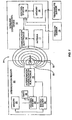
- FIG. 1 illustrates a wireless communication device and communication system that may be used with the present invention.
- the wireless communication device 10 is capable of communicating information wirelessly and may include a control system 12, communication electronics 14, and memory 16.
- the wireless communication device 10 may also be known as a radio-frequency identification device (RFID).
- RFID radio-frequency identification device
- the communication electronics 14 is coupled to an antenna 17 for wirelessly communicating information in radio-frequency signals.
- the communication electronics 14 is capable of receiving modulated radio-frequency signals through the antenna 17 and demodulating these signals into information passed to the control system 12.
- the antenna 17 may be any type of antenna, including but not limited to a pole or slot antenna.
- the antenna 17 may be internal or external to the wireless communication device 10.
- the control system 12 may be any type of circuitry or processor that receives and processes information received by the communication electronics 14, including a micro-controller or microprocessor.
- the wireless communication device 10 may also contain a memory 16 for storage of information. Such information may be any type of information about goods, objects, or articles of manufacture, including but not limited to identification, tracking, environmental information, such as pressure and temperature, and other pertinent information.
- the memory 16 may be electronic memory, such as random access memory (RAM), read-only memory (ROM), flash memory, diode, etc., or the memory 16 may be mechanical memory, such as a switch, dipswitch, etc.
- the control system 12 may also be coupled to sensors that sense environmental information concerning the wireless communication device 10.
- the control system 12 may be coupled to a pressure sensor 18 to sense the pressure on the wireless communication device 10 and/or its surroundings.
- the control system 12 may also be coupled to a temperature sensor 19 to sense the temperature of the wireless communication device 10 or the ambient temperature around the wireless communication device 10. More information on different types of pressure sensors 18 that can be used to couple to the control system are disclosed in U.S. Patent Nos. 6,299,349 and 6,272,936 , entitled “Pressure and temperature sensor” and “Pressure sensor,” respectively, both of which are incorporated herein by reference in their entirety.
- the temperature sensor 19 may be contained within the wireless communication device 10, or external to the wireless communication device 10.
- the temperature sensor 19 may be any variety of temperature sensing elements, such as a thermistor or chemical device.
- One such temperature sensor 19 is described in U.S. Patent No. 5,959,524 , entitled “Temperature sensor,” incorporated herein by reference in its entirety.
- the temperature sensor 19 may also be incorporated into the wireless communication device 10 or its control system 12, like that described in U.S. Patent No. 5,961,215 , entitled “Temperature sensor integral with microprocessor and methods of using same,” incorporated herein by reference in its entirety.
- the present invention is not limited to any particular type of temperature sensor 19.
- Some wireless communication devices 10 are termed “active” devices in that they receive and transmit data using their own energy source coupled to the wireless communication device 10.
- a wireless communication device 10 may use a battery for power as described in U.S. Patent No. 6,130,602 entitled “Radio frequency data communications device,” or may use other forms of energy, such as a capacitor as described in U.S. Patent No. 5,833,603 , entitled “Implantable biosensing transponder.” Both of the preceding patents are incorporated herein by reference in their entirety.
- wireless communication devices 10 are termed “passive” devices meaning that they do not actively transmit and therefore may not include their own energy source for power.
- One type of passive wireless communication device 10 is known as a "transponder.”
- a transponder effectively transmits information by reflecting back a received signal from an external communication device, such as an interrogation reader.
- An example of a transponder is disclosed in U.S. Patent No. 5,347,280 , entitled “Frequency diversity transponder arrangement,” incorporated herein by reference in its entirety.
- Another example of a transponder is described in co-pending International Patent Application No. WO 02/07085 , entitled “Wireless communication device and method,” incorporated herein by reference in its entirety.
- FIG. 1 depicts communication between a wireless communication device 10 and an interrogation reader 20.
- the interrogation reader 20 may include a control system 22, an interrogation communication electronics 24, memory 2 6, and an interrogation antenna 28.
- the interrogation antenna 28 may be any type of antenna, including a pole antenna or a slot antenna.
- the interrogation reader 20 may also contain its own internal energy source 30, or the interrogation reader 20 may be powered through an external power source.
- the energy source 30 may include batteries, a capacitor, solar cell or other medium that contains energy.
- the energy source 30 may also be rechargeable.
- a timer 23 may also be coupled to the control system 22 for performing tasks that require timing operations.
- the interrogation reader 20 communicates with the wireless communication device 10 by emitting an electronic signal 32 modulated by the interrogation communication electronics 24 through the interrogation antenna 28.
- the interrogation antenna 28 may be any type of antenna that can radiate a signal 32 through a field 34 so that a reception device, such as a wireless communication device 10, can receive such signal 32 through its own antenna 17.
- the field 34 may be electro-magnetic, magnetic, or electric.
- the signal 32 may be a message containing information and/or a specific request for the wireless communication device 10 to perform a task or communicate back information.
- the communication electronics 14 are energized by the energy in the signal 32, thereby energizing the wireless communication device 10.
- the wireless communication device 10 remains energized so long as its antenna 17 is in the field 34 of the interrogation reader 20.
- the communication electronics 14 demodulates the signal 32 and sends the message containing information and/or request to the control system 12 for appropriate actions.
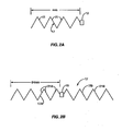
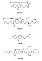
- FIG. 2A illustrates a first embodiment of a wave antenna 17 coupled to a wireless communication device 10 for wireless communication.
- This embodiment illustrates a monopole wave antenna 17.
- the wave antenna 17 is formed by a conducting material, such as a wire or foil for example, that is bent in alternating sections to form a series of peaks and valleys. Any type of material can be used to form the wave antenna 17 so long as the material can conduct electrical energy.
- a wave antenna 17 in its broadest form is a conductor that is bent (either a relatively sharp bend as in the embodiments of Figures 2A, 2B , 3 , 4A, 4B, 4C , 5A, 5B , or a relatively curved bend as in the embodiments of Figures 6A, 6B, 6C, 6D . 7 , 8A, 8B, 8C , 8D, 8E , 8F , 9A, 9B, 9C , 9D, 9E, 9F , 10A, 10B , 10C, 10D and 11 ) in at least one position at (through) an angle less than 180 degrees to form at least two different sections 21.
- the monopole wave antenna 17 in this embodiment contains seven alternating bends to form a saw-tooth wave shape.
- the monopole wave antenna 17 is coupled, by either a direct or reactive coupling, to an input port (not shown) on the wireless communication device 10 to provide an antenna 17 for wireless communications. Since the wireless communication device 10 contains another input port that is coupled to the monopole wave antenna 17, this additional input port is grounded.
- a wave antenna 17 may be particularly advantageous to use with a wireless communication device 10 in lieu of a straight antenna.
- One advantage of a wave antenna 17 is that it is tolerant to stretching without substantial risk of damage or breakage to the conductor. Certain types of goods, objects, or articles of manufacture may encounter a force, such as stretching or compression, during their manufacture and/or normal use. If a wireless communication device 10 uses a straight conductor as antenna 17 and is attached to goods, objects, or articles of manufacture that are subjected to a force during their manufacture or use, the antenna 17 may be damaged or broken when the good, object or article of manufacture is subjected to such force. If the antenna 17 is damaged or broken, this may cause the wireless communication device 10 to be incapable of wireless communication since a change in the length or shape of the conductor in the antenna 17 may change the operating frequency of the antenna 17.
- the impedance of a straight conductor antenna 17 is dependant on the type, size, and shape of the conductor.
- the length of the antenna 17 is the primary variable that determines the operating frequency of the antenna 17.
- a wave antenna 17 can also be varied in other ways not possible in a straight conductor antenna 17.
- other variables exist in the design of the antenna in addition to the type, size, shape and length of the conductor.
- the impedance of a wave antenna 17 can also be varied by varying the length of the individual sections 21 of the conductor making up the wave antenna 17, the angle between these individual sections 21 and the phase, period and amplitude of the sections 21, in addition to the traditional variables available in straight conductor antennas 17.
- a wave antenna 17 provides the ability to alter and select additional variables not possible in straight conductor antennas 17 that affect the impedance of the antenna 17, thereby creating a greater likelihood that a wave antenna's 17 impedance can be designed to more closely match the impedance of the wireless communication device 10.
- the type of materials attached to the wave antenna 17 and the material's dielectric properties also vary the impedance and operating frequency of the wave antenna 17.
- These additional variables should also be taken into account in the final design of the wave antenna 17.
- the reactive cross-coupling that occurs between different sections 21 of the wave antenna 17 also contribute to greater impedance matching capability of the wave antenna 17 to a wireless communication device 10. More information on impedance matching between a wireless communication device 10 and an antenna 17 for efficient transfer of energy is disclosed in International Patent Application No. WO 01/73675 , entitled "Remote communication using slot antenna,” incorporated herein by reference in its entirety.
- Figure 2B illustrates a wave antenna 17 similar to that illustrated in Figure 2A ; however, the wave antenna in Figure 2B is a dipole wave antenna 17.
- Two conductors 17A, 17B are coupled to the wireless communication device 10 to provide wireless communications.
- the length of the conductors 17A, 17B that form the dipole wave antenna 17 are each 84 millimeters in length.
- the dipole wave antenna 17 operates at a frequency of 915 MHz.
- the lengths of the individual sections 21 and the angles between the individual sections 21 that make up the dipole wave antenna 17 are the same; however, they do not have to be.
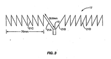
- Figure 3 illustrates another embodiment of a wave antenna 17 where the lengths of the individual sections 21 and the angle between the individual sections 21 are not the same.
- Two conductors are coupled to the wireless communication device 10 to create a dipole wave antenna 17.
- the first conductor is comprised out of two sections 21A, 21C, each having a different number of sections 21 and lengths.
- the two sections 21A, 21C are also symmetrically contained in the second conductor 21B, 21D. This causes the wave antenna 17 to act as a dipole antenna that resonates and receives signals at two different operating frequencies so that the wireless communication device 10 is capable of communicating at two different frequencies.
- the first symmetrical sections 21A, 21B are 30.6 millimeters or ⁇ /4 in length and are coupled to the wireless commnnication device 10 so that the wave antenna 17 is capable of receiving 2.45GHz signals.
- the second symmetrical sections 21C, 21D are coupled to the first sections 21A, 21B, respectively, to form a second dipole antenna for receiving signals at a second frequency.
- the second sections 21C, 21D are 70 millimeters in length and are coupled to the first sections 21A, 21B, respectively, to form lengths that are designed to receive 915 MHz signals.
- bends in the conductor in the wave antenna 17 are not constant. The bends in the wave antenna 17 that are made upward are made at an angle of less than 180 degrees. The bends in the wave antenna 17 that are made downward are made at an angle of 180 degrees.
- bends in sections 21 of the conductor it is permissible for bends in sections 21 of the conductor to be 180 degrees so long as all of the sections 21 in the conductor are not bent at 180 degrees with respect to adjacent sections 21. If all of the sections 21 in the conductor are bent at 180 degrees, then the conductor will effectively be a straight conductor antenna 17 and not a wave antenna 17.
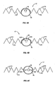
- Figure 4A illustrates another embodiment of the wave antenna 17 coupled to the wireless communication device 10 wherein the wireless communication device 10 is configured to receive signals at two different frequencies.
- a wave antenna 17 similar the wave antenna 17 illustrated in Figure 2B is coupled to the wireless communication device 10 to form a dipole wave antenna 17.
- a resonating ring 40 is also capacitively coupled to the wireless communication device 10 to provide a second antenna 17 that operates at a second and different frequency from the operating frequency of the dipole wave antenna 17.
- the resonating ring 40 may be constructed out of any type of material so long as the material is conductive.
- This embodiment may be particularly advantageous if it is necessary for the wireless communication device 10 to be capable of wirelessly communicating regardless of the force, such as stretching or compression, exerted on the wave antenna 17.
- the resonating ring 40 is designed to remain in its original shape regardless of the application of any force that may be placed on the wireless communication device 10 or a good, object, or article of manufacture that contains the wireless communication device 10.
- the length of the wave antenna 17 may change, thereby changing the operating frequency of the wave antenna 17.
- the new operating frequency of the wave antenna 17 may be sufficiently different from the normal operating frequency such that wave antenna 17 and the wireless communication device 10 could not receive and/or demodulate signals sent by the interrogation reader 20.
- the resonating ring 40 is capable of receiving signals 32 regardless of the state of the wave antenna 17.
- Figure 4B also illustrates an embodiment of the present invention employing a dipole wave antenna 17 that operates at 915 MHz and a resonating ring 40 that operates at 2.45GHz.
- the dipole wave antenna 17 and the resonating ring 40 are both coupled to the wireless communication device 10 to allow the wireless communication device 10 to operate at two different frequencies.
- the conductors of the dipole wave antenna 17 are looped around the resonating ring 40 at a first inductive turn 42A and a second inductive turn 42B. In this manner, any force placed on the dipole wave antenna 17 will place such force on the resonating ring 40 instead of the wireless communication device 10.
- This embodiment may be advantageous in cases where a force, placed on the dipole wave antenna 17 without providing a relief mechanism other than the wireless communication device 10 itself would possibly cause the dipole wave antenna 17 to disconnect from the wireless communication device 10, thus causing the wireless communication device 10 to be unable to wirelessly communicate.
- the resonating ring 40 may be constructed out of a stronger material than the connecting point between the dipole wave antenna 17 and the wireless communication device 10, thereby providing the ability to absorb any force placed on the dipole wave antenna 17 without damaging the resonating ring 40.
- This embodiment may also be particularly advantageous if the wireless communication device 10 is placed on a good, object or article of manufacture that undergoes force during its manufacture or use, such as a rubber tyre, for example.
- Figure 4C illustrates another embodiment similar to those illustrated in Figures 4A and 4B .
- the resonating ring 40 is directly coupled to the wireless communication device 10
- the dipole wave antenna 17 is directly coupled to the resonating ring 10.
- a first and second conducting attachments 44A, 44B are used to couple the resonating ring 40 to the wireless communication device 10.
- a force exerted on the dipole wave antenna 17 is exerted on and absorbed by the resonating ring 40 rather than wireless communication device 10 so that the wireless communication device 10 is not damaged.
- Figure 5A illustrates another embodiment of the wave antenna 17 that is stretched wherein the bending are at angles close to 180 degrees, but slightly less, to form sections 21 close to each other.
- the coupling between the individual elements in the wave antenna 17 will be strong due to the proximity. Therefore, a small change in stretching of the wave antenna 17 will have a large effect on the operating frequency of the wave antenna 17. Since the change in the operating frequency will be great, it will be easier for a small stretching of the wave antenna 17 to change the operating frequency of the wave antenna 17.
- FIG 5B illustrates the same wave antenna 17 and wireless communication device 10 illustrated in Figure 5A ; however, the wave antenna 17 is not being stretched.
- the bent sections in the wave antenna 17 touch each other to effectively act as a regular dipole antenna without angled sections 21.
- each pole 17A, 17B of the wave antenna 17 in its normal form is 30.6 millimeters long and has an operating frequency of 2.45 GHz such that the wireless communication device 10 is capable of responding to a frequency of 2.45 GHz.
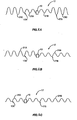
- Figure 6A illustrates a further embodiment of a wave antenna 17 coupled to a wireless communication device 10 for wireless communication.
- This embodiment illustrates a monopole sinusoidal-shaped wave antenna 17.
- the sinusoidal-shaped wave antenna 17 is formed by a conducting material, such as a wire or foil for example, that is curved in alternating sections to form a sinusoidal shape that resembles a sine or cosine waveform.
- the sinusoidal-shaped sections form a series of peaks and valleys in the conductor.
- Any type of material can be used to form the sinusoidal-shaped wave antenna 17 so long as the material can conduct electrical energy, including but not limited to copper, brass, steel, zinc-plated steel, spring brass, and brass coated spring steel.
- the monopole sinusoidal-shaped wave antenna 17 in this embodiment contains seven alternating curves to form a sinusoidal-shaped wave.
- the monopole sinusoidal-shaped wave antenna 17 is coupled, by either a direct or reactive coupling, to an input port (not shown) on the wireless communication device 10 to provide an antenna 17 for wireless communications. Since the wireless communication device 10 contains another input port that is coupled to the monopole sinusoidal-shaped wave antenna 17, this additional input port is grounded.
- Figure 6B illustrates a sinusoidal-shaped wave antenna 17 similar to that illustrated in Figure 6A ; however, the sinusoidal-shaped wave antenna in Figure 6B is a dipole sinusoidal-shaped wave antenna 17.
- Two conductors 17A, 17B are coupled to the wireless communication device 10 to provide wireless communications.
- the length of the conductors 17A, 17B that form the dipole sinusoidal-shaped wave antenna 17 are each 84 millimeters in length.
- the dipole sinusoidal-shaped wave antenna 17 operates at a frequency of 915 MHz.
- the lengths of the individual sections 21 and the angles between the individual sections 21 that make up the dipole sinusoidal-shaped wave antenna 17 are the same; however, they do not have to be.
- Figure 6C illustrates an alternative embodiment of Figure 6A , except that the wave antenna 17 is comprised of sections 21 that are semi-circle shaped. All aspects for the sinusoidal-shaped wave antenna 17 embodiment discussed above and illustrated in Figure 6A is equally applicable for this embodiment.
- Figure 6D illustrates an alternative embodiment of Figure 6B , except that the wave antenna 17 is comprised of sections 21 that are semi-circle shaped. All aspects for the sinusoidal-shaped wave antenna 17 embodiment discussed above and illustrated in Figure 6B is equally applicable for this embodiment.
- Figure 7 illustrates another embodiment of a sinusoidal-shaped wave antenna 17 where the lengths of the individual sections 21 and the angle between the individual sections 21 are not the same.
- Two conductors are coupled to the wireless communication device 10 to create a dipole sinusoidal-shaped wave antenna 17.
- the first conductor is comprised out of two sections 21A, 21C, each having a different number of sections 21 and lengths.
- the two sections 21A, 21C are also symmetrically contained in the second conductor 21B, 21D. This causes the sinusoidal-shaped wave antenna 17 to act as a dipole antenna that resonates and receives signals at two different operating frequencies so that the wireless communication device 10 is capable of communicating at two different frequencies.
- the first symmetrical sections 21A, 21B are 30.6 millimeters or ⁇ /4 in length and are coupled to the wireless communication device 10 so that the sinusoidal-shaped wave antenna 17 is capable of receiving 2.45GHz signals.
- the second symmetrical sections 21C, 21D are coupled to the first sections 21A, 21B, respectively, to form a second dipole antenna for receiving signals at a second frequency.
- the second sections 21C, 21D are 70 millimeters in length and are coupled to the first sections 21A, 21B, respectively, to form lengths that are designed to receive 915 MHz signals.
- curves in the conductor in the sinusoidal-shaped wave antenna 17 are not constant. The curves in the sinusoidal-shaped wave antenna 17 that are made upward are made at an angle of less than 180 degrees. The curves in the sinusoidal-shaped wave antenna 17 that are made downward are made at an angle of 180 degrees.
- wave antenna 17 illustrated in Figure 7 could also be implemented using semi-circle-shaped sections 21.
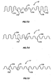
- Figure 8A illustrates another embodiment of a sinusoidal-shaped wave antenna 17 where the amplitudes of the individual sections 21 that form the sinusoidal-shaped wave antenna 17 are not the same.
- Two conductors are coupled to the wireless communication device 10 to create a dipole sinusoidal-shaped wave antenna 17.
- the first conductor is comprised out of two sections 21A, 21C, each having a different number of sections 21 and different amplitudes.
- the two sections 21A, 21C are also symmetrically contained in the second conductor 21B, 21D. This causes the sinusoidal-shaped wave antenna 17 to act as a dipole antenna that resonates and receives signals at two different operating frequencies so that the wireless communication device 10 is capable of communicating at two different frequencies.
- Figure 8B illustrates another embodiment of an asymmetrical sinusoidal-shaped wave antenna 17 where the amplitude of a first pole antenna 17A of the sinusoidal-shaped wave antenna 17 has a different amplitude than the second pole antenna 17B of the sinusoidal-shaped wave antenna 17. More information on asymmetrical pole antennas is disclosed on co-pending International Patent Application No. WO 02/07085 , entitled “Wireless Communication Device and Method,” assigned to the same assignee as the present invention, and incorporated herein by reference in its entirety.
- Figure 8C illustrates another embodiment of an asymmetrical sinusoidal-shaped wave antenna 17 where the length of a first pole antenna 17A of the sinusoidal-shaped wave antenna 17 is of a different length than the second pole antenna 17B of the sinusoidal-shaped wave antenna 17. Note that the embodiments of Figures 8A, 8B, and 8C may be combined to created an asymmetrical dipole wave antenna 17 wherein the pole antennas 17A, 17B contain different lengths, different amplitudes, including different amplitudes within different sections 21, of a pole antenna 17A, 17B.
- Figure 8D illustrates an alternative embodiment of Figure 8A , except that the wave antenna 17 is comprised of sections 21 that are semi-circle shaped. All aspects for the sinusoidal-shaped wave antenna 17 embodiment discussed above and illustrated in Figure 8A is equally applicable for this embodiment.
- Figure 8E illustrates an alternative embodiment of Figure 8B , except that the wave antenna 17 is comprised of sections 21 that are semi-circle shaped. All aspects for the sinusoidal-shaped wave antenna 17 embodiment discussed above and illustrated in Figure 8B is equally applicable for this embodiment.
- Figure 8F illustrates an alternative embodiment of Figure 8C , except that the wave antenna 17 is comprised of sections 21 that are semi-circle shaped. All aspects for the sinusoidal-shaped wave antenna 17 embodiment discussed above and illustrated in Figure 8C is equally applicable for this embodiment.
- Figures 8D, 8E, and 8F may be combined to created an asymmetrical dipole wave antenna 17 wherein the pole antennas 17A, 17B contain different lengths, different amplitudes, including different amplitudes within different sections 21, of a pole antenna 17A, 17B.
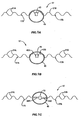
- Figure 9A illustrates another embodiment of the sinusoidal-shaped wave antenna 17 coupled to the wireless communication device 10 wherein the wireless communication device 10 is configured to receive signals at two different frequencies.
- a sinusoidal-shaped wave antenna 17 similar the sinusoidal-shaped wave antenna 17 illustrated in Figure 6B is coupled to the wireless communication device 10 to form a dipole sinusoidal-shaped wave antenna 17.
- a resonating ring 40 is also capacitively coupled to the wireless communication device 10 to provide a second antenna 17 that operates at a second and different frequency from the operating frequency of the dipole sinusoidal-shaped wave antenna 17.
- the resonating ring 40 may be constructed out of any type of material so long as the material is conductive.
- Figure 9B also illustrates an embodiment of the present invention employing a dipole sinusoidal-shaped wave antenna 17 that operates at 915 MHz and a resonating ring 40 that operates at 2.45GHz.
- the dipole sinusoidal-shaped wave antenna 17 and the resonating ring 40 are both coupled to the wireless communication device 10 to allow the wireless communication device 10 to operate at two different frequencies.
- the conductors of the dipole sinusoidal-shaped wave antenna 17 are looped around the resonating ring 40 at a first inductive turn 42A and a second inductive turn 42B. In this manner, any force placed on the dipole sinusoidal-shaped wave antenna 17 will place such force on the resonating ring 40 instead of the wireless communication device 10.
- Figure 9C illustrates another embodiment similar to those illustrated in Figures 9A and 9B .
- the resonating ring 40 is directly coupled to the wireless communication device 10
- the dipole sinusoidal-shaped wave antenna 17 is directly coupled to the resonating ring 10.
- a first and second conducting attachments 44A, 44B are used to couple the resonating ring 40 to the wireless communication device 10.
- a force exerted on the dipole sinusoidal-shaped wave antenna 17 is exerted on and absorbed by the resonating ring 40 rather than wireless communication device 10 so that the wireless communication device 10 is not damaged.
- Figure 9D illustrates an alternative embodiment of Figure 9A , except that the wave antenna 17 is comprised of sections 21 that are semi-circle shaped. All aspects for the sinusoidal-shaped wave antenna 17 embodiment discussed above and illustrated in Figure 9A is equally applicable for this embodiment.
- Figure 9E illustrates an alternative embodiment of Figure 9B , except that the wave antenna 17 is comprised of sections 21 that are semi-circle shaped. All aspects for the sinusoidal-shaped wave antenna 17 embodiment discussed above and illustrated in Figure 9B is equally applicable for this embodiment.
- Figure 9F illustrates an alternative embodiment of Figure 9C , except that the wave antenna 17 is comprised of sections 21 that are semi-circle shaped. All aspects for the sinusoidal-shaped wave antenna 17 embodiment discussed above and illustrated in Figure 9C is equally applicable for this embodiment.
- Figure 10A illustrates another embodiment of the sinusoidal-shaped wave antenna 17 that is stretched wherein the curves in the conductor are at angles close to 180 degrees, but slightly less, to form sections 21 close to each other.
- the embodiment is similar to that of Figure 5A .
- the coupling between the individual elements in the sinusoidal-shaped wave antenna 17 will be strong due to the proximity. Therefore, a small change in stretching of the sinusoidal-shaped wave antenna 17 will have a large effect on the operating frequency of the sinusoidal-shaped wave antenna 17. Since the change in the operating frequency will be great, it will be easier for a small stretching of the sinusoidal-shaped wave antenna 17 to change the operating frequency of the sinusoidal-shaped wave antenna 17.
- FIG 10B illustrates the same sinusoidal-shaped wave antenna 17 and wireless communication device 10 illustrated in Figure 10A ; however, the sinusoidal-shaped wave antenna 17 is not being stretched.
- this sinusoidal-shaped wave antenna 17 is not being stretched, the curved sections in the sinusoidal-shaped wave antenna 17 touch each other to effectively act as a regular dipole antenna without angled sections 21.
- each pole 17A, 17B of the sinusoidal-shaped wave antenna 17 in its normal form is 30.6 millimeters long and has an operating frequency of 2.45 GHz such that the wireless communication device 10 is capable of responding to a frequency of 2.45 GHz.
- Figure 10C illustrates an alternative embodiment of Figure 10A , except that the wave antenna 17 is comprised of sections 21 that are semi-circle shaped. All aspects for the sinusoidal-shaped wave antenna 17 embodiment discussed above and illustrated in Figure 10A is equally applicable for this embodiment.
- Figure 10D illustrates an alternative embodiment of Figure 10B , except that the wave antenna 17 is comprised of sections 21 that are semi-circle shaped. All aspects for the sinusoidal-shaped wave antenna 17 embodiment discussed above and illustrated in Figure 10B is equally applicable for this embodiment
- Figure 11 illustrates an alternative embodiment of the conductive section 21 of the wave antenna 17 wherein the width of the section 21 is dynamically altered along the length of the shape of the section 21.
- the conductive section 21 could be modified from a constant diameter by squeezing in a die. This embodiment spreads the bending effect along the conductive section 21 so that the wave antenna 17 is less susceptible to breaking. For example, the majority of the angular bend in the conductive section 21 occurs at the peak 33 of the conductive section 21 making the peak 31 the most likely place for the wave antenna 17 to break. However, if the peak 33 section of the conductive section 21 is made thicker, and a series of areas on either side of the peak are made thinner, the bend angle is spread over the bend more thereby reducing the probability of breakage.
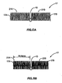
- Figure 12A illustrates one type of article of manufacture that undergoes force during its manufacture and use and that may include a wireless communication device 10 and wave antenna 17 like that illustrated in Figures 5A, 5B , 10A, 10B , 10C, and 10D .
- This embodiment includes a rubber tyre 50 well known in the prior art that is used on transportation vehicles.
- the tyre 50 is designed to be pressurized with air when placed inside a tyre 50 mounted on a vehicle wheel forming a seal between the wheel and the tyre 50.
- the tyre 50 is comprised of a tread surface 52 that has a certain defined thickness 53.
- the tread surface 52 has a left outer side 54, a right outer side 56 and an orifice 58 in the center where the tyre 50 is designed to fit on a wheel.
- the left outer side 54 and right outer side 56 are curved downward at angles substantially perpendicular to the plane of the tread surface 52 to form a left outer wall 60 and a right outer wall 62.
- a left inner wall 64 and a right inner wall (not shown) on the inside of right outer wall 62 are also formed as well.
- a steel belt 68 may also be included inside the rubber of the tyre 50 under the surface of the tread surface 52 for increased performance and life. More information on the construction and design of a typical tyre 50 is disclosed in U.S. Patent No. 5,554,242 , entitled "Method for making a multi-component tyre," incorporated herein by reference in its entirety.
- a wireless communication device 10 and dipole wave antenna 17 are attached on the inner surface of the tyre 50 on the inner side of the tread surface 52.
- the rubber in the tyre 50 undergoes a lamination process whereby the tyre 50 may be stretched up to approximately 1.6 times its normal size and then shrunk back down to the normal dimensions of a wheel.
- the wireless communication device 10 and antenna 17 must be able to withstand the stretching and shrinking that a tyre 50 undergoes without being damaged.
- the wave antenna 17 of the present invention is particularly suited for this application since the wave antenna 17 can stretch and compress without damaging the conductor of the sinusoidal-shaped wave antenna 17.
- a tyre 50 is inflated with a gas, such as air, to a pressure during its normal operation. If the wireless communication device 10 and antenna 17 are placed inside the tread surface 52 or inside the tyre 50, the wireless communication device 10 and antenna 17 will stretch and compress depending on the pressure level in the tyre 50. The more pressure contained in the tyre 50, the more the tyre 50 will stretch.
- a gas such as air
- any wireless communication device 10 and antenna 17 that is contained inside the tyre 50 or inside the rubber of the tyre 50 must be able to withstand this stretching without being damaged and/or affecting the proper operation of the wireless communication device 10.
- Figure 12B illustrates the same tyre illustrated in Figure 12A .
- the tyre 50 is under a pressure and has stretched the dipole wave antenna 17. Because the dipole wave antenna 17 is capable of stretching without being damaged or broken, the dipole wave antenna 17 is not damaged and does not break when the tyre 50 is stretched when subjected to a pressure.
- the wave antenna 17 placed inside the tyre 50 could also be a monopole wave antenna 17, as illustrated in Figures 2A , 6A or 6C , or any other variation of the wave antenna 17, including the wave antennas 17 illustrated in Figures 2B , 3 , 4A-4C , 5A , 5B , 6B , 6D , 7 , 8A-8F , 9A-9F , 10A-10D , and 11 .
- the wireless communication device 10 and wave antenna 17 could be provided anywhere on the inside of the tyre 50, including inside the thickness 53 of the tread surface 52, the left inner wall 64 or the right inner wall (not shown) on the inside of right outer wall 62.
- the length of the wave antenna 17 for optimum coupling is affected by the electrical properties of the material surrounding, and in contact with, the conductive portions of the antenna 17. Since the rubber of the tyre 50 may contain large amounts of "carbon black", a relatively conductive material, an insulating material having the necessary electrical properties, may be required to encapsulate the metal of the antenna 17 with a non-conductive coating (not shown) to insulate it from the rubber of the tyre 50. In other cases the length of the antenna 17 elements must be tuned in length to match the electrical properties of the surrounding material, as is well known issue with antennas.
- wave antenna 17 discussed above and illustrated in Figure 11 may be sinusoidal-shaped and semi-circle shaped.
- Figure 13 illustrates a flowchart process wherein the interrogation reader 20 is designed to communicate with the wireless communication device 10 and wave antenna 17 to determine when the pressure of the tyre 50 has reached a certain designed threshold pressure. Because a wave antenna 17 changes length based on the force exerted on its conductors, a wave antenna 17 will stretch if placed inside a tyre 50 as the pressure inside the tyre 50 rises.
- the wave antenna 17 can be designed so that the length of the wave antenna 17 only reaches a certain designated length to be capable of receiving signals at the operating frequency of the interrogation reader 20 when the tyre 50 reaches a certain threshold pressure.
- the process starts (block 70), and the interrogation reader 20 emits a signal 32 through the field 34 as discussed previously for operation of the interrogation reader 20 and wireless communication device 10 illustrated in Figure 1 .
- the interrogation reader 20 checks to see if a response communication has been received from the wireless communication device 10 (decision 74). If no response signal is received by the interrogation reader 20 from the wireless communication device 10, the interrogation reader 20 continues to emit the signal 32 through field 34 in a looping fashion (block 72) until a response is received.
- the interrogation reader 20 can report that the tyre 50 containing the wireless communication device 10 and wave antenna 17 has reached a certain threshold pressure.
- the wave antennas 17 may be any of the wave antennas 17 illustrated in Figures 2B , 3 , 4A-4C , 5A , 5B , 6A-6D , 7 , 8A-8F , 9A-9F , 10A-10D and 11 .
- Figure 14 illustrates one embodiment of a reporting system 77 that may be provided for the interrogation reader 20.
- the interrogation reader 20 may be coupled to a reporting system 77.
- This reporting system 77 may be located in close proximity to the interrogation reader 20, and may be coupled to the interrogation reader 20 by either a wired or wireless connection.
- the reporting system 77 may be a user interface or other computer system that is capable of receiving and/or storing data communications received from an interrogation reader 20.
- This information may be any type of information received from a wireless communication device 10, including but not limited to identification information, tracking information, and/or environmental information concerning the wireless communication device 10 and/or its surroundings, such as pressure and temperature. The information may be used for any purpose.
- identification, tracking, temperature, force and/or pressure information concerning a tyre 50 during its manufacture may be communicated to the reporting system 77 which may then be used for tracking, quality control, and supply-chain management. If the information received by the reporting system is not normal or proper, the reporting system 77 may control the manufacturing operations to stop and/or change processes during manufacture and/or alert personnel in charge of the manufacturing process.
- the reporting system 77 may also communicate information received from the wireless communication device 10, via the interrogation reader 20, to a remote system 78 located remotely from the reporting system 77 and/or the interrogation reader 20.
- the communication between the reporting system 77 and the remote system 78 may be through wired communication, wireless communication, modem communication or other networking communication, such as the Internet.
- the interrogation reader 20 may communicate the information received from the wireless communication device 10 directly to the remote system 78 rather than first reporting the information through the reporting system 77 using the same or similar communication mediums as may be used between the reporting system 77 and the remote system 78.
- Figure 15 illustrates a method of manufacturing a wave antenna 17 and assembling of the wave antenna 17 to wireless communication devices 10.
- the process involves eight total steps. Each of the steps is labeled in circled numbers illustrated in Figure 15 .
- the first step of the process involves passing an antenna 17 conductor wire or foil through cogs 120 to create the alternating curves in the antenna conductor 17 to form the wave antenna 17.
- the cogs 120 are comprised of a top cog 120A and a bottom cog 120B.
- the top cog 120A rotates clockwise, and the bottom cog 120B rotates counterclockwise.
- Each cog 120A, 120B has a periphery such that each of the cogs 120A, 120B interlock with each other as they rotate.
- alternating curved bends are placed in the antenna conductor 17 to form peaks 121 and valleys 122 in the antenna conductor 17 to form the wave antenna 17.
- the second step of the process involves placing tin solder on portions of the wave antenna 17 so that a wireless communication device 10 can be soldered and attached to the wave antenna 17 in a later step.
- a soldering station 123 is provided and is comprised of a first tinning position 123A and a second tinning position 123B.
- the first tinning position 123A and second tinning position 123B raise upward to place tin solder on the left side of the peak 124A and an adjacent right side of the peak 124B so that the wireless communication device 10 can be soldered to the wave antenna 17 in the third step of the process.
- the process may also use glue, induction welding, or other suitable adhesive, instead of solder, to attach the wireless communication device 10 to the wave antenna 17.
- the third step of the process involves attaching a wireless communication device 10 to the wave antenna 17.
- a wireless communication device is attached to the left side of the peak 124A and the right side of the peak 124B at the points of the tin solder.
- An adhesive 126 is used to attach the leads or pins (not shown) of the wireless communication device 10 to the tin solder, and solder paste is added to the points where the wireless communication device 10 attach to the tin solder on the wave antenna 17 to conductively attach the wireless communication device 10 to the wave antenna 17. Note that when the wireless communication device 10 is attached to the wave antenna 17, the peak remains on the wireless communication device 10 that causes a short 128 between the two input ports (not shown) of the wireless communication device 10 and the two wave antennas 17 coupled to the wireless communication device 10.
- the fourth step in the process involves passing the wireless communication device 10 as connected to the wave antenna 17 through a hot gas re-flow soldering process well known to one of ordinary skill in the art to securely attach the solder between the leads of the wireless communication device 10 and the wave antenna 17.
- the fifth step in the process involves the well-known process of cleaning away any excess solder that is unused and left over during the previous soldering.
- the sixth step in the process involves removing the short 128 between the two wave antennas 17 left by the peak 124 of the wave antenna 17 from the third step in the process.
- the short 128 may or may not cause the wireless communication device 10 to not properly operate to receive signals and re-modulate response signals. If the wireless communication device 10 operation is not affected by this short 128, this step can be skipped in the process.
- the seventh step in the process involves encapsulating the wireless communication device 10.
- the wireless communication device 10 is typically in the form of an RF integrated circuit chip that is encapsulated with a hardened, non-conductive material, such as a plastic or epoxy, to protect the inside components of the chip from the environment.
- An additional encapsulating material, such as epoxy, may also be added over the bonding points of the wireless communication device 10 to the wave antenna 17 to add additional mechanical strain relief.
- the eighth and last step involves winding wireless communication devices 10 as attached on the wave antenna 17 onto a reel 130.
- the wireless communication devices 10 and wave antenna 17 are contained on a strip since the wave antenna 17 conductor has not been yet cut.
- the wireless communication device 10 and attached wave antenna 17 can be unwound from the reel 130 and the wave antenna 17 conductor cut in the middle between two consecutive wireless communication devices 10 to form separate wireless communication device 10 and dipole wave antenna 17 devices.
- the wave antenna 17 may be sinusoidal-shaped, semi-circle shaped, or may have relatively sharp bends as in the embodiments of Figures 2A, 2B , 3 , 4A-4C , 5A, 5B , the latter requiring sharper teeth on the cogs 120A, 120B instead of the rounded teeth to produce the curved bends.
- CNC computer numerical controller
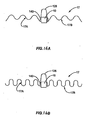
- Figure 16A illustrates the short 128 left on the wireless communication device 10 and sinusoidal-shaped wave antenna 17 as a tuning inductance.
- Some UHF wireless communication devices 10 operate best when a direct current (DC) short, in the form of a tuning inductance, is present across the wireless communication device 10 and, therefore, the process of removing the short 128 can be omitted.
- Figure 16A illustrates an alternative embodiment of the sinusoidal-shaped wave antenna 17 and wireless communication device 10 where an uneven cog 120 has been used in step 1 of the process illustrated in Figure 15 to produce an extended loop short 128 across the wireless communication device 10. This gives the required amount of inductance for best operation of the wireless communication device 10 as the sinusoidal-shaped wave antenna 17 and the short 128 are in parallel.
- Figure 16B illustrates an alternative embodiment of Figure 16A , except that the wave antenna 17 is comprised of sections 21 that are semi-circle shaped. All aspects for the sinusoidal-shaped wave antenna 17 embodiment discussed above and illustrated in Figure 16A is equally applicable for this embodiment. An embodiment with relatively sharp bends as in the antennas of Figures 2A and 2B is also of course possible.
- the present invention is not limited to applications involving a vehicle tyre. It should also be understood that the present invention is not limited to any particular type of component, including but not limited to the wireless communication device 10 and its components, the wave antenna 17, the interrogation reader 20 and its components, the pressure sensor 18, the temperature sensor 19, the resonating ring 40, the tyre 50 and its components, the reporting system 77, the remote system 78, the wheel 100 and its components, the cogs 120, the soldering station 123, and the adhesive 124.
- couple, coupled, or coupling is defined as either a direct connection or a reactive coupling.
- Reactive coupling is defined as either capacitive or inductive coupling.
- the wave antenna 17 discussed in this application may be sinusoidal-shaped or semi-circle shaped.
Landscapes
- Engineering & Computer Science (AREA)
- Physics & Mathematics (AREA)
- Theoretical Computer Science (AREA)
- Microelectronics & Electronic Packaging (AREA)
- Computer Hardware Design (AREA)
- General Physics & Mathematics (AREA)
- Mechanical Engineering (AREA)
- Computer Networks & Wireless Communication (AREA)
- Electromagnetism (AREA)
- Arrangements For Transmission Of Measured Signals (AREA)
- Details Of Aerials (AREA)
- Support Of Aerials (AREA)
- Radar Systems Or Details Thereof (AREA)
- Variable-Direction Aerials And Aerial Arrays (AREA)
Applications Claiming Priority (3)
| Application Number | Priority Date | Filing Date | Title |
|---|---|---|---|
| US10/012,206 US6630910B2 (en) | 2001-10-29 | 2001-10-29 | Wave antenna wireless communication device and method |
| US10/228,180 US6903704B2 (en) | 2001-10-29 | 2002-08-26 | Wave antenna wireless communication device and method |
| EP02785803A EP1446766B1 (fr) | 2001-10-29 | 2002-10-29 | Dispositif de radiocommunications a antenne ondulee, et procede correspondant |
Related Parent Applications (1)
| Application Number | Title | Priority Date | Filing Date |
|---|---|---|---|
| EP02785803A Division EP1446766B1 (fr) | 2001-10-29 | 2002-10-29 | Dispositif de radiocommunications a antenne ondulee, et procede correspondant |
Publications (3)
| Publication Number | Publication Date |
|---|---|
| EP1942448A2 true EP1942448A2 (fr) | 2008-07-09 |
| EP1942448A3 EP1942448A3 (fr) | 2008-09-10 |
| EP1942448B1 EP1942448B1 (fr) | 2014-06-25 |
Family
ID=21753850
Family Applications (1)
| Application Number | Title | Priority Date | Filing Date |
|---|---|---|---|
| EP08006372.0A Expired - Lifetime EP1942448B1 (fr) | 2001-10-29 | 2002-10-29 | Dispositif et procédé de communication sans fil d'antenne à ondes |
Country Status (4)
| Country | Link |
|---|---|
| US (7) | US6630910B2 (fr) |
| EP (1) | EP1942448B1 (fr) |
| AT (1) | ATE470915T1 (fr) |
| DE (1) | DE60236682D1 (fr) |
Cited By (1)
| Publication number | Priority date | Publication date | Assignee | Title |
|---|---|---|---|---|
| EP2377699A1 (fr) | 2010-04-16 | 2011-10-19 | Delta Electronics, Inc. | Système de surveillance de pression pneumatique bidirectionnelle et procédé utilisant des fréquences très élevées dites UHF |
Families Citing this family (120)
| Publication number | Priority date | Publication date | Assignee | Title |
|---|---|---|---|---|
| US7342496B2 (en) | 2000-01-24 | 2008-03-11 | Nextreme Llc | RF-enabled pallet |
| US8077040B2 (en) | 2000-01-24 | 2011-12-13 | Nextreme, Llc | RF-enabled pallet |
| US7190319B2 (en) | 2001-10-29 | 2007-03-13 | Forster Ian J | Wave antenna wireless communication device and method |
| US8266465B2 (en) | 2000-07-26 | 2012-09-11 | Bridgestone Americas Tire Operation, LLC | System for conserving battery life in a battery operated device |
| US7161476B2 (en) | 2000-07-26 | 2007-01-09 | Bridgestone Firestone North American Tire, Llc | Electronic tire management system |
| US6951596B2 (en) | 2002-01-18 | 2005-10-04 | Avery Dennison Corporation | RFID label technique |
| US6630910B2 (en) * | 2001-10-29 | 2003-10-07 | Marconi Communications Inc. | Wave antenna wireless communication device and method |
| WO2003038747A2 (fr) * | 2001-10-29 | 2003-05-08 | Marconi Intellectual Property (Us) Inc | Dispositif de radiocommunications a antenne beverage, et procede correspondant |
| DE10154494A1 (de) * | 2001-11-08 | 2003-05-22 | Continental Ag | Sende- und/oder Empfangseinrichtung zum Einbau in elastische Strukturen sowie Antennen hierfür |
| DE10164488A1 (de) * | 2001-12-29 | 2003-07-10 | Bosch Gmbh Robert | Vorrichtung zum Senden und/oder Empfangen von Daten, Reifen für ein Kraftfahrzeug, Sende- und/oder Empfangseinrichtung und System zur drahtlosen Übertragung von Daten |
| FR2837985B1 (fr) * | 2002-04-02 | 2004-05-21 | Commissariat Energie Atomique | Antenne receptrice morcelee |
| FR2837748A1 (fr) * | 2002-04-02 | 2003-10-03 | Michelin Soc Tech | Pneumatique dote d'une antenne receptrice |
| US7239287B2 (en) * | 2002-04-24 | 2007-07-03 | Mineral Lassen Llc | Wireless communication device having conductive elements antenna |
| DE10223800A1 (de) * | 2002-05-29 | 2003-12-18 | Continental Ag | Transponder zum Einbau in oder auf die Oberfläche von Gegenständen |
| US7100432B2 (en) * | 2002-06-06 | 2006-09-05 | Mineral Lassen Llc | Capacitive pressure sensor |
| US20040159383A1 (en) * | 2002-06-11 | 2004-08-19 | Adamson John David | Method for embedding a radio frequency antenna in a tire, and an antenna for embedding in a tire |
| SE0300127D0 (sv) * | 2003-01-17 | 2003-01-17 | Imego Ab | Indicator arrangement |
| US7091841B2 (en) * | 2003-02-19 | 2006-08-15 | Michelin Recherche Et Technique, S.A. | Tire electronics assembly having a multi-frequency antenna |
| US6870506B2 (en) * | 2003-06-04 | 2005-03-22 | Auden Techno Corp. | Multi-frequency antenna with single layer and feeding point |
| GB0318134D0 (en) * | 2003-08-01 | 2003-09-03 | Gatan Uk | Specimen tip and tip holder assembly |
| EP1526385B1 (fr) * | 2003-10-21 | 2006-08-09 | STMicroelectronics S.r.l. | Méthode pour déterminer les caractéristiques physiques d'un pneumatique |
| US7259678B2 (en) * | 2003-12-08 | 2007-08-21 | 3M Innovative Properties Company | Durable radio frequency identification label and methods of manufacturing the same |
| US6999028B2 (en) * | 2003-12-23 | 2006-02-14 | 3M Innovative Properties Company | Ultra high frequency radio frequency identification tag |
| US7317901B2 (en) | 2004-02-09 | 2008-01-08 | Motorola, Inc. | Slotted multiple band antenna |
| DE102004008929A1 (de) * | 2004-02-24 | 2005-09-01 | Bayerische Motoren Werke Ag | Fahrzeugreifen mit Stahlgürteldrähten sowie einer im Bereich der Lauffläche angeordneten Dipol-Antenne |
| JP2007527174A (ja) * | 2004-03-05 | 2007-09-20 | コーニンクレッカ フィリップス エレクトロニクス エヌ ヴィ | Rfidタグ用のアンテナ構造体 |
| US7500307B2 (en) | 2004-09-22 | 2009-03-10 | Avery Dennison Corporation | High-speed RFID circuit placement method |
| US20070241982A1 (en) * | 2004-09-30 | 2007-10-18 | Alan Stigliani | Contoured triangular dipole antenna |
| US7688206B2 (en) * | 2004-11-22 | 2010-03-30 | Alien Technology Corporation | Radio frequency identification (RFID) tag for an item having a conductive layer included or attached |
| EP1674298A1 (fr) | 2004-12-23 | 2006-06-28 | Société de Technologie Michelin | Système pour la communication de données sans fil entre un véhicule et ses penumatiques |
| EP1674301A3 (fr) | 2004-12-23 | 2010-04-28 | Société de Technologie Michelin | Système de communication de données sans fil entre un véhicule et ses pneumatiques |
| US7545272B2 (en) | 2005-02-08 | 2009-06-09 | Therasense, Inc. | RF tag on test strips, test strip vials and boxes |
| FI121521B (fi) * | 2005-02-17 | 2010-12-15 | Upm Raflatac Oy | Transponderin viritysmenetelmä ja transponderi |
| US7623034B2 (en) | 2005-04-25 | 2009-11-24 | Avery Dennison Corporation | High-speed RFID circuit placement method and device |
| US7501947B2 (en) * | 2005-05-04 | 2009-03-10 | Tc License, Ltd. | RFID tag with small aperture antenna |
| US7551070B2 (en) | 2005-09-02 | 2009-06-23 | Gm Global Technology Operations, Inc. | Wireless sensing system |
| US20070164865A1 (en) * | 2005-11-04 | 2007-07-19 | Gerald Giasson | Security sensor system |
| US20070114889A1 (en) * | 2005-11-21 | 2007-05-24 | Honeywell International | Chip level packaging for wireless surface acoustic wave sensor |
| US7555826B2 (en) | 2005-12-22 | 2009-07-07 | Avery Dennison Corporation | Method of manufacturing RFID devices |
| TWI310689B (en) * | 2006-02-09 | 2009-06-11 | Ind Tech Res Inst | Flexible antenna device for energy transmission,method for control the same and method for energy transmission of the same,flexible antenna module for wireless energy transmission and an energy transmission apparatus containing the same and method for en |
| US7668129B2 (en) * | 2006-03-30 | 2010-02-23 | Intel Corporation | Learning mechanism to configure power save parameters for automatic power save delivery |
| GB2437115B (en) * | 2006-04-13 | 2008-10-29 | Motorola Inc | Antenna arrangement and an RF communication terminal incorporating the arrangement |
| US8196829B2 (en) * | 2006-06-23 | 2012-06-12 | Fractus, S.A. | Chip module, sim card, wireless device and wireless communication method |
| KR100763596B1 (ko) * | 2006-06-30 | 2007-10-05 | 한국전자통신연구원 | 루프 구조와 헬리컬 구조를 이용한 안테나, 이를 이용한rfⅰd 태그 및 안테나 임피던스 정합 방법 |
| US7659857B2 (en) * | 2006-07-05 | 2010-02-09 | King Patrick F | System and method for providing a low and narrow-profile radio frequency identification (RFID) tag |
| DE102006039113A1 (de) * | 2006-08-21 | 2008-03-06 | Robert Bosch Gmbh | Reifensensormodul und Verfahren zu seiner Herstellung |
| US20080055045A1 (en) * | 2006-08-31 | 2008-03-06 | 3M Innovative Properties Company | Rfid tag including a three-dimensional antenna |
| US7564356B1 (en) | 2006-10-06 | 2009-07-21 | Tc License, Ltd. | Interdigit AC coupling for RFID tags |
| USD589500S1 (en) * | 2006-11-02 | 2009-03-31 | First Impression Systems, Llc | EAS antenna |
| US7914058B2 (en) * | 2006-12-18 | 2011-03-29 | The Goodyear Tire & Rubber Company | Picking apparatus for an electronic device |
| US7767052B2 (en) * | 2006-12-18 | 2010-08-03 | The Goodyear Tire & Rubber Company | Method of assembling an electronic device into a tire |
| US7868841B2 (en) * | 2007-04-11 | 2011-01-11 | Vubiq Incorporated | Full-wave di-patch antenna |
| US8049624B2 (en) * | 2007-04-18 | 2011-11-01 | Semiconductor Energy Laboratory Co., Ltd. | Wireless communication method |
| US7768407B2 (en) | 2007-06-22 | 2010-08-03 | Avery Dennison Corporation | Foldable RFID device interposer and method |
| US7880614B2 (en) * | 2007-09-26 | 2011-02-01 | Avery Dennison Corporation | RFID interposer with impedance matching |
| US20090085750A1 (en) * | 2007-09-27 | 2009-04-02 | 3M Innovative Properties Company | Extended RFID tag |
| US8289163B2 (en) * | 2007-09-27 | 2012-10-16 | 3M Innovative Properties Company | Signal line structure for a radio-frequency identification system |
| US8717244B2 (en) * | 2007-10-11 | 2014-05-06 | 3M Innovative Properties Company | RFID tag with a modified dipole antenna |
| US7864131B2 (en) * | 2007-11-29 | 2011-01-04 | Knight Eric A | Versatile wire antenna and method |
| US8633821B2 (en) * | 2007-12-03 | 2014-01-21 | Avery Dennison Corporation | Dual use RFID/EAS device |
| US8847764B2 (en) | 2007-12-05 | 2014-09-30 | Avery Dennison Corporation | RFID system with distributed read structure |
| US7786868B2 (en) * | 2007-12-11 | 2010-08-31 | Avery Dennison Corporation | RFID device with multiple passive operation modes |
| JP5114177B2 (ja) * | 2007-12-12 | 2013-01-09 | 富士通テン株式会社 | 情報記録装置 |
| JP4871949B2 (ja) | 2007-12-20 | 2012-02-08 | 原田工業株式会社 | パッチアンテナ装置 |
| JP4797031B2 (ja) * | 2008-02-08 | 2011-10-19 | 日立オートモティブシステムズ株式会社 | 圧力測定装置およびタイヤ圧力監視システム |
| US7847697B2 (en) * | 2008-02-14 | 2010-12-07 | 3M Innovative Properties Company | Radio frequency identification (RFID) tag including a three-dimensional loop antenna |
| US7872613B2 (en) * | 2008-04-01 | 2011-01-18 | Pacesetter, Inc. | Enhanced implantable helical antenna system and method |
| US7876282B2 (en) * | 2008-04-01 | 2011-01-25 | Pacesetter, Inc. | Enhanced implantable di-pole antenna system and method |
| BRPI0822605B1 (pt) | 2008-04-29 | 2019-04-02 | Compagnie Generale Des Etablissements Michelin | Dispositivo de identificação por radiofrequência, e, método para montagem de um dispositivo de identificação por radiofrequência. |
| JP4524318B2 (ja) | 2008-05-27 | 2010-08-18 | 原田工業株式会社 | 車載用ノイズフィルタ |
| JP5114325B2 (ja) * | 2008-07-08 | 2013-01-09 | 原田工業株式会社 | 車両用ルーフマウントアンテナ装置 |
| JP5256935B2 (ja) * | 2008-08-26 | 2013-08-07 | 富士通株式会社 | Idタグの製造方法 |
| US8144069B2 (en) * | 2008-10-02 | 2012-03-27 | Bogdan Sadowski | Hidden wideband antenna |
| JP4832549B2 (ja) * | 2009-04-30 | 2011-12-07 | 原田工業株式会社 | 空間充填曲線を用いる車両用アンテナ装置 |
| JP4955094B2 (ja) * | 2009-11-02 | 2012-06-20 | 原田工業株式会社 | パッチアンテナ |
| CN103038072B (zh) * | 2010-04-09 | 2016-08-10 | 倍耐力轮胎股份公司 | 轮胎传感器装置 |
| US9122967B2 (en) | 2010-04-14 | 2015-09-01 | Technologies Roi, Llc | Radio frequency identification tags and methods employing ceramic components, which may be suitable for use in extreme environmental conditions |
| FR2961353B1 (fr) * | 2010-06-15 | 2013-07-26 | Commissariat Energie Atomique | Antenne pour milieu humide |
| FR2961354B1 (fr) | 2010-06-15 | 2012-06-01 | Commissariat Energie Atomique | Antenne haute frequence |
| FR2963852B1 (fr) * | 2010-08-11 | 2013-10-11 | Soc Tech Michelin | Antenne pour un dispositif electronique d'un pneumatique |
| FR2963851B1 (fr) | 2010-08-11 | 2017-04-21 | Soc De Tech Michelin | Procede de fabrication d'une antenne pour un dispositif electronique d'un pneumatique |
| WO2012027320A2 (fr) * | 2010-08-23 | 2012-03-01 | Landy Aaron Toth | Système et procédé de surveillance d'un site chirurgical |
| US8816917B2 (en) | 2011-01-12 | 2014-08-26 | Harada Industry Co., Ltd. | Antenna device |
| JP5274597B2 (ja) | 2011-02-15 | 2013-08-28 | 原田工業株式会社 | 車両用ポールアンテナ |
| USD749063S1 (en) | 2011-02-16 | 2016-02-09 | Callas Enterprises Llc | Combined mat and eas antenna |
| USD715274S1 (en) | 2011-02-16 | 2014-10-14 | Callas Enterprises, LLC | Combined mat and EAS antenna |
| US8907774B2 (en) | 2011-03-01 | 2014-12-09 | Bendix Commercial Vehicle Systems Llc | System and method for monitoring tire condition |
| JP5654917B2 (ja) | 2011-03-24 | 2015-01-14 | 原田工業株式会社 | アンテナ装置 |
| FR2986372B1 (fr) * | 2012-01-31 | 2014-02-28 | Commissariat Energie Atomique | Procede d'assemblage d'un element a puce micro-electronique sur un element filaire, installation permettant de realiser l'assemblage |
| USD726696S1 (en) | 2012-09-12 | 2015-04-14 | Harada Industry Co., Ltd. | Vehicle antenna |
| US10032659B2 (en) * | 2012-12-28 | 2018-07-24 | Sunedison Semiconductor Limited (Uen201334164H) | Methods and systems for preventing unsafe operations |
| USD749062S1 (en) | 2013-01-02 | 2016-02-09 | Callas Enterprises Llc | Combined floor mat and EAS antenna |
| US9067466B2 (en) | 2013-01-30 | 2015-06-30 | Bendix Commercial Vehicle Systems Llc | Diversity antenna |
| JP6161487B2 (ja) * | 2013-09-24 | 2017-07-12 | 峰光電子株式会社 | 読み取りセンサー及び管理システム |
| US20150349432A1 (en) * | 2014-06-02 | 2015-12-03 | Physical Devices, Llc | Wavelength compressed antennas |
| US9582750B2 (en) * | 2014-12-22 | 2017-02-28 | Avery Dennison Retail Information Services, Llc | RFID devices with multi-frequency antennae |
| CN105226381A (zh) * | 2015-09-09 | 2016-01-06 | 天津理工大学 | 一款小型化超高频弯折偶极子天线 |
| US9929779B2 (en) * | 2015-12-01 | 2018-03-27 | Maxim Integrated Products, Inc. | Power adaptive dual mode card emulation system for NFC and RFID application |
| US9779351B1 (en) * | 2016-02-29 | 2017-10-03 | Brunswick Corporation | Marine vessel hull with embedded wireless identification device |
| FR3066721B1 (fr) * | 2017-05-23 | 2019-06-07 | Continental Automotive France | Procede d'identification d'au moins un emetteur de surveillance de la pression d'un pneumatique d'un vehicule automobile par association avec une des roues dudit vehicule automobile |
| US10559884B2 (en) * | 2017-10-03 | 2020-02-11 | Intermec, Inc. | Wideband RFID tag antenna |
| WO2019186067A1 (fr) * | 2018-03-30 | 2019-10-03 | Compagnie Generale Des Etablissements Michelin | Transpondeur radiofrequence pour pneumatique |
| US12339272B2 (en) | 2019-03-27 | 2025-06-24 | Lyten, Inc. | Sensors incorporated into building materials to detect physical characteristic changes |
| US11555761B1 (en) * | 2019-03-27 | 2023-01-17 | Lyten, Inc. | Sensors incorporated into elastomeric components to detect physical characteristic changes |
| US11479062B2 (en) * | 2019-03-27 | 2022-10-25 | Lyten, Inc. | Tuned radio frequency (RF) resonant materials and material configurations for sensing in a vehicle |
| US12270785B2 (en) | 2019-03-27 | 2025-04-08 | Lyten, Inc. | Water droplet sensing systems and methods |
| US12196636B2 (en) | 2019-03-27 | 2025-01-14 | Lyten, Inc. | Sensors incorporated into airborne vehicle components to detect physical characteristic changes |
| US12265058B2 (en) | 2019-03-27 | 2025-04-01 | Lyten, Inc. | Sensors incorporated into adhesive material |
| US11965803B2 (en) | 2019-03-27 | 2024-04-23 | Lyten, Inc. | Field deployable resonant sensors |
| US12313570B2 (en) | 2019-03-27 | 2025-05-27 | Lyten, Inc. | Leaky coaxial resonant sensor systems and methods |
| US11585731B2 (en) | 2019-03-27 | 2023-02-21 | Lyten, Inc. | Sensors incorporated into semi-rigid structural members to detect physical characteristic changes |
| US12317466B2 (en) | 2019-03-27 | 2025-05-27 | Lyten, Inc. | Frequency selective metamaterial for protective enclosures |
| US11769954B2 (en) | 2019-08-27 | 2023-09-26 | Tensorcom, Inc. | Method and apparatus for millimeter wave antenna array |
| JP7457519B2 (ja) * | 2020-02-18 | 2024-03-28 | 株式会社ブリヂストン | 航空機用タイヤ |
| DE102021211347A1 (de) * | 2021-10-07 | 2023-04-13 | Aktiebolaget Skf | Übertragungsriemen |
| CN117766977A (zh) * | 2022-09-16 | 2024-03-26 | 手持产品公司 | 射频识别(rfid)打印机天线 |
| DE102022210494A1 (de) | 2022-10-04 | 2024-04-04 | Aktiebolaget Skf | Übertragungsriemen |
| TWI872455B (zh) * | 2023-02-13 | 2025-02-11 | 系統電子工業股份有限公司 | 充電式胎壓偵測系統及其方法 |
| US20240275608A1 (en) | 2023-02-15 | 2024-08-15 | Lyten, Inc. | Method to learn precise sensing fingerprints based on machine learning integration |
| US20240403594A1 (en) * | 2023-06-01 | 2024-12-05 | Ccl Label, Inc. | Antennas in radio frequency identification (rfid) tags |
Citations (14)
| Publication number | Priority date | Publication date | Assignee | Title |
|---|---|---|---|---|
| DE317753C (fr) | ||||
| GB2220101A (en) | 1988-06-02 | 1989-12-28 | Samsung Electronics Co Ltd | Wire bonding |
| US4911217A (en) | 1989-03-24 | 1990-03-27 | The Goodyear Tire & Rubber Company | Integrated circuit transponder in a pneumatic tire for tire identification |
| WO1993018493A1 (fr) | 1992-03-03 | 1993-09-16 | N.V. Nederlandsche Apparatenfabriek Nedap | Procede de fabrication d'une etiquette de detection a hautes frequences avec un minimum de composants electroniques |
| US5347280A (en) | 1993-07-02 | 1994-09-13 | Texas Instruments Deutschland Gmbh | Frequency diversity transponder arrangement |
| US5554242A (en) | 1986-06-02 | 1996-09-10 | The Goodyear Tire & Rubber Company | Method for making a multi-component tire |
| US5833603A (en) | 1996-03-13 | 1998-11-10 | Lipomatrix, Inc. | Implantable biosensing transponder |
| US5959524A (en) | 1995-11-15 | 1999-09-28 | Heraeus Electro-Nite International N.V. | Temperature sensor |
| US5961215A (en) | 1997-09-26 | 1999-10-05 | Advanced Micro Devices, Inc. | Temperature sensor integral with microprocessor and methods of using same |
| US6130602A (en) | 1996-05-13 | 2000-10-10 | Micron Technology, Inc. | Radio frequency data communications device |
| US6272936B1 (en) | 1998-02-20 | 2001-08-14 | Tekscan, Inc | Pressure sensor |
| WO2001073675A2 (fr) | 2000-03-25 | 2001-10-04 | Marconi Corporation Plc | Dispositif d'identification de contenant |
| US6299349B1 (en) | 1996-11-15 | 2001-10-09 | Steinel Ag | Pressure and temperature sensor |
| WO2002007085A1 (fr) | 2000-07-18 | 2002-01-24 | Marconi Corporation P.L.C. | Dispositif et procede de communication sans fil |
Family Cites Families (96)
| Publication number | Priority date | Publication date | Assignee | Title |
|---|---|---|---|---|
| US1451472A (en) * | 1921-06-01 | 1923-04-10 | Ralph E H Pomeroy | Pulverizing mill |
| US2292303A (en) * | 1940-05-11 | 1942-08-04 | Goodman Mfg Co | Mine locomotive |
| US2709220A (en) * | 1954-01-25 | 1955-05-24 | Nat Electronic Mfg Corp | Extensible and retractible antenna |
| US3202985A (en) * | 1961-09-26 | 1965-08-24 | Gen Electric | True three-dimensional display system |
| US3508274A (en) * | 1966-12-14 | 1970-04-21 | Raymond B Kesler | Motor driven portable dipole antenna |
| US3689929A (en) * | 1970-11-23 | 1972-09-05 | Howard B Moody | Antenna structure |
| US3778833A (en) * | 1971-07-29 | 1973-12-11 | Us Navy | Magnetic-electronic position encoder |
| US4250509A (en) * | 1979-08-29 | 1981-02-10 | Harris Corporation | Circularly polarized zigzag antenna |
| DE3200444A1 (de) * | 1982-01-09 | 1983-07-21 | Wilhelm Sihn jr. KG, 7532 Niefern-Öschelbronn | Teleskopantenne mit betaetigungseinrichtung |
| JPS5972530U (ja) * | 1982-11-08 | 1984-05-17 | 日産自動車株式会社 | タイヤ空気圧センサ |
| US4494591A (en) | 1983-09-14 | 1985-01-22 | Shopsmith, Inc. | Tilting table for a woodworking tool |
| US4739516A (en) * | 1986-01-17 | 1988-04-19 | A. Van Brackel & Sons, Inc. | Frequency tuned antenna assembly |
| JPS62206902A (ja) * | 1986-03-06 | 1987-09-11 | Asmo Co Ltd | 電動アンテナ装置 |
| US4866456A (en) * | 1986-07-16 | 1989-09-12 | Fulton Manufacturing Corporation | Horizon-to-horizon satellite antenna drive mechanism |
| DE3736803A1 (de) | 1987-10-30 | 1989-05-11 | Vdo Schindling | Am rad eines kraftfahrzeuges montiertes pruefelement zur ueberwachung des reifeninnendruckes |
| JPH01116899U (fr) | 1988-01-30 | 1989-08-07 | ||
| JPH0279602A (ja) | 1988-09-16 | 1990-03-20 | Nippon Telegr & Teleph Corp <Ntt> | マイクロストリップアンテナ |
| US5181975A (en) * | 1991-03-27 | 1993-01-26 | The Goodyear Tire & Rubber Company | Integrated circuit transponder with coil antenna in a pneumatic tire for use in tire identification |
| US5218861A (en) * | 1991-03-27 | 1993-06-15 | The Goodyear Tire & Rubber Company | Pneumatic tire having an integrated circuit transponder and pressure transducer |
| US5274393A (en) * | 1991-09-23 | 1993-12-28 | Allied-Signal Inc. | Adjustable helical antenna for a VHF radio |
| FR2683951A1 (fr) * | 1991-11-14 | 1993-05-21 | Michelin & Cie | Structure d'antenne adaptee pour la communication avec une etiquette electronique implantee dans un pneumatique. |
| US5479171A (en) * | 1993-04-27 | 1995-12-26 | Texas Instruments Deutschland Gmbh | Extended range RF-ID transponder |
| EP0639472B1 (fr) * | 1993-08-18 | 1997-10-15 | Bridgestone Corporation | Bandage pneumatique comportant un transpondeur, appareil et méthode pour enregistrer et lire sur un transpondeur |
| US6087930A (en) * | 1994-02-22 | 2000-07-11 | Computer Methods Corporation | Active integrated circuit transponder and sensor apparatus for transmitting vehicle tire parameter data |
| US5731754A (en) * | 1994-06-03 | 1998-03-24 | Computer Methods Corporation | Transponder and sensor apparatus for sensing and transmitting vehicle tire parameter data |
| US5682143A (en) | 1994-09-09 | 1997-10-28 | International Business Machines Corporation | Radio frequency identification tag |
| US6452553B1 (en) * | 1995-08-09 | 2002-09-17 | Fractal Antenna Systems, Inc. | Fractal antennas and fractal resonators |
| ES2236745T3 (es) * | 1995-08-09 | 2005-07-16 | Fractal Antenna Systems Inc. | Antenas resonadores y elementos de carga fractales. |
| US7019695B2 (en) * | 1997-11-07 | 2006-03-28 | Nathan Cohen | Fractal antenna ground counterpoise, ground planes, and loading elements and microstrip patch antennas with fractal structure |
| US6104349A (en) * | 1995-08-09 | 2000-08-15 | Cohen; Nathan | Tuning fractal antennas and fractal resonators |
| DE19605836C1 (de) * | 1996-02-16 | 1997-01-23 | Siemens Ag | Verfahren zum Betreiben einer Diebstahlschutzeinrichtung und Diebstahlschutzeinrichtung |
| US6016127A (en) * | 1996-06-26 | 2000-01-18 | Howell Laboratories, Inc. | Traveling wave antenna |
| US6097347A (en) * | 1997-01-29 | 2000-08-01 | Intermec Ip Corp. | Wire antenna with stubs to optimize impedance for connecting to a circuit |
| CH691098A5 (fr) * | 1997-03-24 | 2001-04-12 | Em Microelectronic Marin Sa | Structure monolithique de circuits intégrés et de bobine d'antenne, munie d'un anneau de protection périphérique. |
| EP0884796A3 (fr) | 1997-06-11 | 1999-03-24 | Matsushita Electric Industrial Co., Ltd. | Antenne comprenant de portions courbés ou incurvés |
| JPH11154819A (ja) | 1997-11-19 | 1999-06-08 | Furukawa Electric Co Ltd:The | 小型ヘリカルアンテナ |
| CA2312153A1 (fr) | 1997-12-09 | 1999-06-17 | The Goodyear Tire & Rubber Company | Antenne pour repondeur radio |
| WO1999029522A1 (fr) | 1997-12-09 | 1999-06-17 | The Goodyear Tire & Rubber Company | Pneumatique muni d'une antenne pour repeteur radio |
| US6281794B1 (en) * | 1998-01-02 | 2001-08-28 | Intermec Ip Corp. | Radio frequency transponder with improved read distance |
| US6061036A (en) | 1998-02-03 | 2000-05-09 | Ericsson, Inc. | Rigid and flexible antenna |
| TW464582B (en) * | 1998-02-17 | 2001-11-21 | Lincoln Global Inc | Welding wire and method of making same |
| US6320509B1 (en) * | 1998-03-16 | 2001-11-20 | Intermec Ip Corp. | Radio frequency identification transponder having a high gain antenna configuration |
| US6147606A (en) * | 1998-03-26 | 2000-11-14 | Intermec Ip Corp. | Apparatus and method for radio frequency transponder with improved read distance |
| SE513055C2 (sv) | 1998-04-24 | 2000-06-26 | Intenna Technology Ab | Flerbandsantennanordning |
| US6023250A (en) * | 1998-06-18 | 2000-02-08 | The United States Of America As Represented By The Secretary Of The Navy | Compact, phasable, multioctave, planar, high efficiency, spiral mode antenna |
| SE512524C2 (sv) | 1998-06-24 | 2000-03-27 | Allgon Ab | En antennanordning, en metod för framställning av en antennenordning och en radiokommunikationsanordning inkluderande en antennanordning |
| DE19828397A1 (de) * | 1998-06-25 | 1999-12-30 | Siemens Ag | Abstimmbare Antenne mit getrennten Strahlerteilen und Verfahren zu ihrer Herstellung |
| AU5809099A (en) * | 1998-09-11 | 2000-04-03 | Motorola, Inc. | Radio frequency identification tag apparatus and related method |
| JP3324522B2 (ja) * | 1998-09-16 | 2002-09-17 | 日本電気株式会社 | 可変利得増幅回路及び利得制御方法 |
| KR100308189B1 (ko) * | 1998-09-17 | 2001-11-30 | 윤종용 | 코어셀기반의집적회로의테스트용이도를증가시키기위한바운더리스캔회로 |
| US6140974A (en) * | 1998-10-20 | 2000-10-31 | Nortel Networks Limited | Antenna arrangement |
| US6100804A (en) * | 1998-10-29 | 2000-08-08 | Intecmec Ip Corp. | Radio frequency identification system |
| US6285342B1 (en) * | 1998-10-30 | 2001-09-04 | Intermec Ip Corp. | Radio frequency tag with miniaturized resonant antenna |
| US6366260B1 (en) * | 1998-11-02 | 2002-04-02 | Intermec Ip Corp. | RFID tag employing hollowed monopole antenna |
| US6262692B1 (en) * | 1999-01-13 | 2001-07-17 | Brady Worldwide, Inc. | Laminate RFID label and method of manufacture |
| JP3485823B2 (ja) * | 1999-01-14 | 2004-01-13 | 三菱電機株式会社 | 携帯無線機 |
| US6043746A (en) * | 1999-02-17 | 2000-03-28 | Microchip Technology Incorporated | Radio frequency identification (RFID) security tag for merchandise and method therefor |
| US6278413B1 (en) * | 1999-03-29 | 2001-08-21 | Intermec Ip Corporation | Antenna structure for wireless communications device, such as RFID tag |
| US6388567B1 (en) * | 1999-04-29 | 2002-05-14 | Bridgestone/Firestone North American Tire, Llc | Combination monitoring device and patch for a pneumatic tire and method of installing the same |
| US6474380B1 (en) * | 1999-04-29 | 2002-11-05 | Bridgestone/Firestone North American Tire, Llc | Pneumatic tire and monitoring device including dipole antenna |
| US6208244B1 (en) * | 1999-04-29 | 2001-03-27 | Bridgestone/Firestone Research, Inc. | Combination monitoring device and patch for a pneumatic tire and method of installing the same with a coupled antenna |
| CH693394A5 (fr) | 1999-05-07 | 2003-07-15 | Njc Innovations | Carte à puce comportant une antenne. |
| JP3639767B2 (ja) * | 1999-06-24 | 2005-04-20 | 株式会社村田製作所 | 表面実装型アンテナおよびそれを用いた通信機 |
| US6198442B1 (en) * | 1999-07-22 | 2001-03-06 | Ericsson Inc. | Multiple frequency band branch antennas for wireless communicators |
| AU6210700A (en) * | 1999-08-18 | 2001-03-13 | Ericsson Inc. | A dual band bowtie/meander antenna |
| US6899153B1 (en) * | 1999-11-15 | 2005-05-31 | The Goodyear Tire & Rubber Company | Mounting transponders and antennas in pneumatic tires |
| AU2025000A (en) * | 1999-11-15 | 2001-05-30 | Goodyear Tire And Rubber Company, The | Mounting transponders and antennas in pneumatic tires |
| EP1259390B1 (fr) * | 2000-03-03 | 2008-11-05 | Continental Automotive GmbH | Pneumatique dote d'un detecteur et procede permettant de determiner une grandeur d'usure d'un tel pneumatique |
| US6371178B1 (en) * | 2000-03-09 | 2002-04-16 | Bridgestone/Firestone North American Tire, Llc | Method of providing electrical power to an embedded electronic device in a tire using close proximity electromagnetic coupling |
| US7190319B2 (en) * | 2001-10-29 | 2007-03-13 | Forster Ian J | Wave antenna wireless communication device and method |
| US6535175B2 (en) * | 2000-06-01 | 2003-03-18 | Intermec Ip Corp. | Adjustable length antenna system for RF transponders |
| US7161476B2 (en) * | 2000-07-26 | 2007-01-09 | Bridgestone Firestone North American Tire, Llc | Electronic tire management system |
| EP2272688B1 (fr) * | 2000-07-26 | 2012-02-01 | Bridgestone Americas Tire Operations, LLC | Système électronique de gestion de pneus |
| US6424315B1 (en) * | 2000-08-02 | 2002-07-23 | Amkor Technology, Inc. | Semiconductor chip having a radio-frequency identification transceiver |
| JP2002064329A (ja) | 2000-08-15 | 2002-02-28 | Sony Corp | 無線通信装置 |
| US6429817B1 (en) * | 2000-10-03 | 2002-08-06 | Bellsouth Intellectual Property Corporation | Retractable antenna for portable telephone |
| US6713676B2 (en) * | 2000-11-15 | 2004-03-30 | Texas Instruments Incorporated | System and method for converting a DC input voltage to a DC output voltage |
| US6480110B2 (en) * | 2000-12-01 | 2002-11-12 | Microchip Technology Incorporated | Inductively tunable antenna for a radio frequency identification tag |
| FR2817509B1 (fr) * | 2000-12-05 | 2003-08-29 | Trw France | Systeme de mesure de parametres de roue et detecteur de mesure pour un tel systeme |
| DE10107531A1 (de) | 2000-12-23 | 2002-06-27 | Nuedling Franz C Basaltwerk | Verfahren zum Herstellen von Formsteinen, Vorrichtung und Formstein |
| US6459413B1 (en) * | 2001-01-10 | 2002-10-01 | Industrial Technology Research Institute | Multi-frequency band antenna |
| JP4152595B2 (ja) * | 2001-01-11 | 2008-09-17 | 横浜ゴム株式会社 | トランスポンダ及びそのシステム |
| JP4501097B2 (ja) * | 2001-01-12 | 2010-07-14 | 横浜ゴム株式会社 | タイヤ装着用トランスポンダ及びトランスポンダ装着タイヤの製造方法 |
| US6463798B2 (en) * | 2001-01-17 | 2002-10-15 | Microchip Technology Incorporated | Tire inflation pressure monitoring and location determining method and apparatus |
| US20020116992A1 (en) * | 2001-02-26 | 2002-08-29 | Trw Inc. | System and method for monitoring wear of a vehicle component |
| US6683537B2 (en) * | 2001-03-29 | 2004-01-27 | The Goodyear Tire And Rubber Company | System of apparatus for monitoring a tire condition value in a pneumatic tire |
| US20020190852A1 (en) * | 2001-06-14 | 2002-12-19 | Trw Inc. | Tire pressure monitoring apparatus and method |
| WO2003038747A2 (fr) | 2001-10-29 | 2003-05-08 | Marconi Intellectual Property (Us) Inc | Dispositif de radiocommunications a antenne beverage, et procede correspondant |
| US6630910B2 (en) * | 2001-10-29 | 2003-10-07 | Marconi Communications Inc. | Wave antenna wireless communication device and method |
| US6882318B2 (en) * | 2002-03-04 | 2005-04-19 | Siemens Information & Communications Mobile, Llc | Broadband planar inverted F antenna |
| US20040016487A1 (en) * | 2002-07-24 | 2004-01-29 | Johnson David Allan | Coupled transponder and antenna system and method |
| US6734791B2 (en) * | 2002-07-31 | 2004-05-11 | Michelin Recherche Et Technique S.A. | Electronics component assembly in a tire for remotely monitoring tire conditions |
| US7050017B2 (en) * | 2002-08-14 | 2006-05-23 | King Patrick F | RFID tire belt antenna system and method |
| US7116213B2 (en) * | 2002-11-22 | 2006-10-03 | Michelin Recherche Et Technique S.A. | Acoustic wave device with modulation functionality |
| US6870506B2 (en) * | 2003-06-04 | 2005-03-22 | Auden Techno Corp. | Multi-frequency antenna with single layer and feeding point |
| US6999028B2 (en) * | 2003-12-23 | 2006-02-14 | 3M Innovative Properties Company | Ultra high frequency radio frequency identification tag |
-
2001
- 2001-10-29 US US10/012,206 patent/US6630910B2/en not_active Expired - Lifetime
-
2002
- 2002-08-26 US US10/228,180 patent/US6903704B2/en not_active Expired - Lifetime
- 2002-10-29 DE DE60236682T patent/DE60236682D1/de not_active Expired - Lifetime
- 2002-10-29 AT AT02785803T patent/ATE470915T1/de not_active IP Right Cessation
- 2002-10-29 EP EP08006372.0A patent/EP1942448B1/fr not_active Expired - Lifetime
-
2003
- 2003-02-07 US US10/360,124 patent/US6895655B2/en not_active Expired - Fee Related
- 2003-08-08 US US10/637,326 patent/US7375699B2/en not_active Expired - Lifetime
-
2005
- 2005-04-12 US US11/105,156 patent/US7394438B2/en not_active Expired - Lifetime
-
2008
- 2008-05-23 US US12/126,812 patent/US7746285B2/en not_active Expired - Fee Related
-
2010
- 2010-05-27 US US12/789,337 patent/US7916095B2/en not_active Expired - Fee Related
Patent Citations (14)
| Publication number | Priority date | Publication date | Assignee | Title |
|---|---|---|---|---|
| DE317753C (fr) | ||||
| US5554242A (en) | 1986-06-02 | 1996-09-10 | The Goodyear Tire & Rubber Company | Method for making a multi-component tire |
| GB2220101A (en) | 1988-06-02 | 1989-12-28 | Samsung Electronics Co Ltd | Wire bonding |
| US4911217A (en) | 1989-03-24 | 1990-03-27 | The Goodyear Tire & Rubber Company | Integrated circuit transponder in a pneumatic tire for tire identification |
| WO1993018493A1 (fr) | 1992-03-03 | 1993-09-16 | N.V. Nederlandsche Apparatenfabriek Nedap | Procede de fabrication d'une etiquette de detection a hautes frequences avec un minimum de composants electroniques |
| US5347280A (en) | 1993-07-02 | 1994-09-13 | Texas Instruments Deutschland Gmbh | Frequency diversity transponder arrangement |
| US5959524A (en) | 1995-11-15 | 1999-09-28 | Heraeus Electro-Nite International N.V. | Temperature sensor |
| US5833603A (en) | 1996-03-13 | 1998-11-10 | Lipomatrix, Inc. | Implantable biosensing transponder |
| US6130602A (en) | 1996-05-13 | 2000-10-10 | Micron Technology, Inc. | Radio frequency data communications device |
| US6299349B1 (en) | 1996-11-15 | 2001-10-09 | Steinel Ag | Pressure and temperature sensor |
| US5961215A (en) | 1997-09-26 | 1999-10-05 | Advanced Micro Devices, Inc. | Temperature sensor integral with microprocessor and methods of using same |
| US6272936B1 (en) | 1998-02-20 | 2001-08-14 | Tekscan, Inc | Pressure sensor |
| WO2001073675A2 (fr) | 2000-03-25 | 2001-10-04 | Marconi Corporation Plc | Dispositif d'identification de contenant |
| WO2002007085A1 (fr) | 2000-07-18 | 2002-01-24 | Marconi Corporation P.L.C. | Dispositif et procede de communication sans fil |
Cited By (1)
| Publication number | Priority date | Publication date | Assignee | Title |
|---|---|---|---|---|
| EP2377699A1 (fr) | 2010-04-16 | 2011-10-19 | Delta Electronics, Inc. | Système de surveillance de pression pneumatique bidirectionnelle et procédé utilisant des fréquences très élevées dites UHF |
Also Published As
| Publication number | Publication date |
|---|---|
| US20080235937A1 (en) | 2008-10-02 |
| EP1942448A3 (fr) | 2008-09-10 |
| US6895655B2 (en) | 2005-05-24 |
| US7916095B2 (en) | 2011-03-29 |
| US6630910B2 (en) | 2003-10-07 |
| US7394438B2 (en) | 2008-07-01 |
| US20060050001A1 (en) | 2006-03-09 |
| US20040041739A1 (en) | 2004-03-04 |
| US20030080919A1 (en) | 2003-05-01 |
| US6903704B2 (en) | 2005-06-07 |
| US7375699B2 (en) | 2008-05-20 |
| EP1942448B1 (fr) | 2014-06-25 |
| DE60236682D1 (de) | 2010-07-22 |
| US7746285B2 (en) | 2010-06-29 |
| US20030117334A1 (en) | 2003-06-26 |
| ATE470915T1 (de) | 2010-06-15 |
| US20100231360A1 (en) | 2010-09-16 |
| US20030080918A1 (en) | 2003-05-01 |
Similar Documents
| Publication | Publication Date | Title |
|---|---|---|
| EP1446766B1 (fr) | Dispositif de radiocommunications a antenne ondulee, et procede correspondant | |
| EP1942448B1 (fr) | Dispositif et procédé de communication sans fil d'antenne à ondes | |
| EP1590856B1 (fr) | Dispositif et procede de communication sans fil | |
| EP1539509B1 (fr) | Procede et systeme d'antenne a bande pour pneumatique a identification par radiofrequence | |
| JP7174415B2 (ja) | Rfidタグ、rfidタグ内蔵タイヤ、およびrfidタグの共振周波数を調整する方法 |
Legal Events
| Date | Code | Title | Description |
|---|---|---|---|
| PUAI | Public reference made under article 153(3) epc to a published international application that has entered the european phase |
Free format text: ORIGINAL CODE: 0009012 |
|
| 17P | Request for examination filed |
Effective date: 20080331 |
|
| AC | Divisional application: reference to earlier application |
Ref document number: 1446766 Country of ref document: EP Kind code of ref document: P |
|
| AK | Designated contracting states |
Kind code of ref document: A2 Designated state(s): AT BE BG CH CY CZ DE DK EE ES FI FR GB GR IE IT LI LU MC NL PT SE SK TR |
|
| PUAL | Search report despatched |
Free format text: ORIGINAL CODE: 0009013 |
|
| RIN1 | Information on inventor provided before grant (corrected) |
Inventor name: KING, PATRICK, F. Inventor name: FORSTER, IAN JAMES Inventor name: HORRELL, PETER, ROBERT, GEORGE Inventor name: PFEIFFER, MICHAEL, J. |
|
| AK | Designated contracting states |
Kind code of ref document: A3 Designated state(s): AT BE BG CH CY CZ DE DK EE ES FI FR GB GR IE IT LI LU MC NL PT SE SK TR |
|
| RIN1 | Information on inventor provided before grant (corrected) |
Inventor name: FORSTER, IAN JAMES Inventor name: HORRELL, PETER, ROBERT, GEORGE Inventor name: PFEIFFER, MICHAEL, J. Inventor name: KING, PATRICK, F. |
|
| AKX | Designation fees paid |
Designated state(s): AT BE BG CH CY CZ DE DK EE ES FI FR GB GR IE IT LI LU MC NL PT SE SK TR |
|
| GRAP | Despatch of communication of intention to grant a patent |
Free format text: ORIGINAL CODE: EPIDOSNIGR1 |
|
| INTG | Intention to grant announced |
Effective date: 20140122 |
|
| RIN1 | Information on inventor provided before grant (corrected) |
Inventor name: FORSTER, IAN JAMES Inventor name: PFEIFFER, MICHAEL, J. Inventor name: HORRELL, PETER, ROBERT, GEORGE Inventor name: KING, PATRICK, F. |
|
| GRAS | Grant fee paid |
Free format text: ORIGINAL CODE: EPIDOSNIGR3 |
|
| GRAA | (expected) grant |
Free format text: ORIGINAL CODE: 0009210 |
|
| AC | Divisional application: reference to earlier application |
Ref document number: 1446766 Country of ref document: EP Kind code of ref document: P |
|
| AK | Designated contracting states |
Kind code of ref document: B1 Designated state(s): AT BE BG CH CY CZ DE DK EE ES FI FR GB GR IE IT LI LU MC NL PT SE SK TR |
|
| REG | Reference to a national code |
Ref country code: GB Ref legal event code: FG4D |
|
| REG | Reference to a national code |
Ref country code: CH Ref legal event code: EP |
|
| REG | Reference to a national code |
Ref country code: AT Ref legal event code: REF Ref document number: 675083 Country of ref document: AT Kind code of ref document: T Effective date: 20140715 |
|
| REG | Reference to a national code |
Ref country code: IE Ref legal event code: FG4D |
|
| REG | Reference to a national code |
Ref country code: DE Ref legal event code: R096 Ref document number: 60246392 Country of ref document: DE Effective date: 20140807 |
|
| PG25 | Lapsed in a contracting state [announced via postgrant information from national office to epo] |
Ref country code: FI Free format text: LAPSE BECAUSE OF FAILURE TO SUBMIT A TRANSLATION OF THE DESCRIPTION OR TO PAY THE FEE WITHIN THE PRESCRIBED TIME-LIMIT Effective date: 20140625 Ref country code: GR Free format text: LAPSE BECAUSE OF FAILURE TO SUBMIT A TRANSLATION OF THE DESCRIPTION OR TO PAY THE FEE WITHIN THE PRESCRIBED TIME-LIMIT Effective date: 20140926 Ref country code: CY Free format text: LAPSE BECAUSE OF FAILURE TO SUBMIT A TRANSLATION OF THE DESCRIPTION OR TO PAY THE FEE WITHIN THE PRESCRIBED TIME-LIMIT Effective date: 20140625 |
|
| REG | Reference to a national code |
Ref country code: AT Ref legal event code: MK05 Ref document number: 675083 Country of ref document: AT Kind code of ref document: T Effective date: 20140625 |
|
| REG | Reference to a national code |
Ref country code: NL Ref legal event code: VDEP Effective date: 20140625 |
|
| PG25 | Lapsed in a contracting state [announced via postgrant information from national office to epo] |
Ref country code: SE Free format text: LAPSE BECAUSE OF FAILURE TO SUBMIT A TRANSLATION OF THE DESCRIPTION OR TO PAY THE FEE WITHIN THE PRESCRIBED TIME-LIMIT Effective date: 20140625 |
|
| PG25 | Lapsed in a contracting state [announced via postgrant information from national office to epo] |
Ref country code: EE Free format text: LAPSE BECAUSE OF FAILURE TO SUBMIT A TRANSLATION OF THE DESCRIPTION OR TO PAY THE FEE WITHIN THE PRESCRIBED TIME-LIMIT Effective date: 20140625 Ref country code: CZ Free format text: LAPSE BECAUSE OF FAILURE TO SUBMIT A TRANSLATION OF THE DESCRIPTION OR TO PAY THE FEE WITHIN THE PRESCRIBED TIME-LIMIT Effective date: 20140625 Ref country code: SK Free format text: LAPSE BECAUSE OF FAILURE TO SUBMIT A TRANSLATION OF THE DESCRIPTION OR TO PAY THE FEE WITHIN THE PRESCRIBED TIME-LIMIT Effective date: 20140625 Ref country code: PT Free format text: LAPSE BECAUSE OF FAILURE TO SUBMIT A TRANSLATION OF THE DESCRIPTION OR TO PAY THE FEE WITHIN THE PRESCRIBED TIME-LIMIT Effective date: 20141027 Ref country code: ES Free format text: LAPSE BECAUSE OF FAILURE TO SUBMIT A TRANSLATION OF THE DESCRIPTION OR TO PAY THE FEE WITHIN THE PRESCRIBED TIME-LIMIT Effective date: 20140625 |
|
| PG25 | Lapsed in a contracting state [announced via postgrant information from national office to epo] |
Ref country code: NL Free format text: LAPSE BECAUSE OF FAILURE TO SUBMIT A TRANSLATION OF THE DESCRIPTION OR TO PAY THE FEE WITHIN THE PRESCRIBED TIME-LIMIT Effective date: 20140625 Ref country code: AT Free format text: LAPSE BECAUSE OF FAILURE TO SUBMIT A TRANSLATION OF THE DESCRIPTION OR TO PAY THE FEE WITHIN THE PRESCRIBED TIME-LIMIT Effective date: 20140625 |
|
| REG | Reference to a national code |
Ref country code: DE Ref legal event code: R097 Ref document number: 60246392 Country of ref document: DE |
|
| PG25 | Lapsed in a contracting state [announced via postgrant information from national office to epo] |
Ref country code: DK Free format text: LAPSE BECAUSE OF FAILURE TO SUBMIT A TRANSLATION OF THE DESCRIPTION OR TO PAY THE FEE WITHIN THE PRESCRIBED TIME-LIMIT Effective date: 20140625 Ref country code: IT Free format text: LAPSE BECAUSE OF FAILURE TO SUBMIT A TRANSLATION OF THE DESCRIPTION OR TO PAY THE FEE WITHIN THE PRESCRIBED TIME-LIMIT Effective date: 20140625 |
|
| PLBE | No opposition filed within time limit |
Free format text: ORIGINAL CODE: 0009261 |
|
| STAA | Information on the status of an ep patent application or granted ep patent |
Free format text: STATUS: NO OPPOSITION FILED WITHIN TIME LIMIT |
|
| PG25 | Lapsed in a contracting state [announced via postgrant information from national office to epo] |
Ref country code: MC Free format text: LAPSE BECAUSE OF FAILURE TO SUBMIT A TRANSLATION OF THE DESCRIPTION OR TO PAY THE FEE WITHIN THE PRESCRIBED TIME-LIMIT Effective date: 20140625 Ref country code: LU Free format text: LAPSE BECAUSE OF FAILURE TO SUBMIT A TRANSLATION OF THE DESCRIPTION OR TO PAY THE FEE WITHIN THE PRESCRIBED TIME-LIMIT Effective date: 20141029 |
|
| REG | Reference to a national code |
Ref country code: CH Ref legal event code: PL |
|
| 26N | No opposition filed |
Effective date: 20150326 |
|
| REG | Reference to a national code |
Ref country code: IE Ref legal event code: MM4A |
|
| PG25 | Lapsed in a contracting state [announced via postgrant information from national office to epo] |
Ref country code: LI Free format text: LAPSE BECAUSE OF NON-PAYMENT OF DUE FEES Effective date: 20141031 Ref country code: CH Free format text: LAPSE BECAUSE OF NON-PAYMENT OF DUE FEES Effective date: 20141031 |
|
| PG25 | Lapsed in a contracting state [announced via postgrant information from national office to epo] |
Ref country code: IE Free format text: LAPSE BECAUSE OF NON-PAYMENT OF DUE FEES Effective date: 20141029 |
|
| PG25 | Lapsed in a contracting state [announced via postgrant information from national office to epo] |
Ref country code: BG Free format text: LAPSE BECAUSE OF FAILURE TO SUBMIT A TRANSLATION OF THE DESCRIPTION OR TO PAY THE FEE WITHIN THE PRESCRIBED TIME-LIMIT Effective date: 20140625 |
|
| PG25 | Lapsed in a contracting state [announced via postgrant information from national office to epo] |
Ref country code: BE Free format text: LAPSE BECAUSE OF FAILURE TO SUBMIT A TRANSLATION OF THE DESCRIPTION OR TO PAY THE FEE WITHIN THE PRESCRIBED TIME-LIMIT Effective date: 20140625 Ref country code: TR Free format text: LAPSE BECAUSE OF FAILURE TO SUBMIT A TRANSLATION OF THE DESCRIPTION OR TO PAY THE FEE WITHIN THE PRESCRIBED TIME-LIMIT Effective date: 20140625 |
|
| REG | Reference to a national code |
Ref country code: FR Ref legal event code: PLFP Year of fee payment: 15 |
|
| REG | Reference to a national code |
Ref country code: FR Ref legal event code: PLFP Year of fee payment: 16 |
|
| REG | Reference to a national code |
Ref country code: FR Ref legal event code: PLFP Year of fee payment: 17 |
|
| PGFP | Annual fee paid to national office [announced via postgrant information from national office to epo] |
Ref country code: FR Payment date: 20210921 Year of fee payment: 20 |
|
| PGFP | Annual fee paid to national office [announced via postgrant information from national office to epo] |
Ref country code: GB Payment date: 20210929 Year of fee payment: 20 |
|
| PGFP | Annual fee paid to national office [announced via postgrant information from national office to epo] |
Ref country code: DE Payment date: 20210916 Year of fee payment: 20 |
|
| REG | Reference to a national code |
Ref country code: DE Ref legal event code: R071 Ref document number: 60246392 Country of ref document: DE |
|
| REG | Reference to a national code |
Ref country code: GB Ref legal event code: PE20 Expiry date: 20221028 |
|
| PG25 | Lapsed in a contracting state [announced via postgrant information from national office to epo] |
Ref country code: GB Free format text: LAPSE BECAUSE OF EXPIRATION OF PROTECTION Effective date: 20221028 |