EP1950775A1 - Monolidthischer Keramischer Kondensator - Google Patents
Monolidthischer Keramischer Kondensator Download PDFInfo
- Publication number
- EP1950775A1 EP1950775A1 EP08008922A EP08008922A EP1950775A1 EP 1950775 A1 EP1950775 A1 EP 1950775A1 EP 08008922 A EP08008922 A EP 08008922A EP 08008922 A EP08008922 A EP 08008922A EP 1950775 A1 EP1950775 A1 EP 1950775A1
- Authority
- EP
- European Patent Office
- Prior art keywords
- monolithic ceramic
- ceramic capacitor
- capacitor
- terminal
- size
- Prior art date
- Legal status (The legal status is an assumption and is not a legal conclusion. Google has not performed a legal analysis and makes no representation as to the accuracy of the status listed.)
- Granted
Links
Images


Classifications
-
- H—ELECTRICITY
- H01—ELECTRIC ELEMENTS
- H01G—CAPACITORS; CAPACITORS, RECTIFIERS, DETECTORS, SWITCHING DEVICES, LIGHT-SENSITIVE OR TEMPERATURE-SENSITIVE DEVICES OF THE ELECTROLYTIC TYPE
- H01G4/00—Fixed capacitors; Processes of their manufacture
- H01G4/002—Details
- H01G4/228—Terminals
- H01G4/232—Terminals electrically connecting two or more layers of a stacked or rolled capacitor
-
- H—ELECTRICITY
- H01—ELECTRIC ELEMENTS
- H01G—CAPACITORS; CAPACITORS, RECTIFIERS, DETECTORS, SWITCHING DEVICES, LIGHT-SENSITIVE OR TEMPERATURE-SENSITIVE DEVICES OF THE ELECTROLYTIC TYPE
- H01G4/00—Fixed capacitors; Processes of their manufacture
- H01G4/002—Details
- H01G4/228—Terminals
-
- H—ELECTRICITY
- H05—ELECTRIC TECHNIQUES NOT OTHERWISE PROVIDED FOR
- H05K—PRINTED CIRCUITS; CASINGS OR CONSTRUCTIONAL DETAILS OF ELECTRIC APPARATUS; MANUFACTURE OF ASSEMBLAGES OF ELECTRICAL COMPONENTS
- H05K3/00—Apparatus or processes for manufacturing printed circuits
- H05K3/30—Assembling printed circuits with electric components, e.g. with resistors
- H05K3/32—Assembling printed circuits with electric components, e.g. with resistors electrically connecting electric components or wires to printed circuits
- H05K3/34—Assembling printed circuits with electric components, e.g. with resistors electrically connecting electric components or wires to printed circuits by soldering
- H05K3/341—Surface mounted components
- H05K3/3421—Leaded components
- H05K3/3426—Leaded components characterised by the leads
-
- H—ELECTRICITY
- H01—ELECTRIC ELEMENTS
- H01F—MAGNETS; INDUCTANCES; TRANSFORMERS; SELECTION OF MATERIALS FOR THEIR MAGNETIC PROPERTIES
- H01F27/00—Details of transformers or inductances, in general
- H01F27/28—Coils; Windings; Conductive connections
- H01F27/29—Terminals; Tapping arrangements for signal inductances
- H01F27/292—Surface mounted devices
- H01F2027/295—Surface mounted devices with flexible terminals
-
- H—ELECTRICITY
- H05—ELECTRIC TECHNIQUES NOT OTHERWISE PROVIDED FOR
- H05K—PRINTED CIRCUITS; CASINGS OR CONSTRUCTIONAL DETAILS OF ELECTRIC APPARATUS; MANUFACTURE OF ASSEMBLAGES OF ELECTRICAL COMPONENTS
- H05K2201/00—Indexing scheme relating to printed circuits covered by H05K1/00
- H05K2201/10—Details of components or other objects attached to or integrated in a printed circuit board
- H05K2201/10613—Details of electrical connections of non-printed components, e.g. special leads
- H05K2201/10621—Components characterised by their electrical contacts
- H05K2201/10636—Leadless chip, e.g. chip capacitor or resistor
-
- H—ELECTRICITY
- H05—ELECTRIC TECHNIQUES NOT OTHERWISE PROVIDED FOR
- H05K—PRINTED CIRCUITS; CASINGS OR CONSTRUCTIONAL DETAILS OF ELECTRIC APPARATUS; MANUFACTURE OF ASSEMBLAGES OF ELECTRICAL COMPONENTS
- H05K2201/00—Indexing scheme relating to printed circuits covered by H05K1/00
- H05K2201/10—Details of components or other objects attached to or integrated in a printed circuit board
- H05K2201/10613—Details of electrical connections of non-printed components, e.g. special leads
- H05K2201/10742—Details of leads
- H05K2201/10886—Other details
- H05K2201/10946—Leads attached onto leadless component after manufacturing the component
-
- Y—GENERAL TAGGING OF NEW TECHNOLOGICAL DEVELOPMENTS; GENERAL TAGGING OF CROSS-SECTIONAL TECHNOLOGIES SPANNING OVER SEVERAL SECTIONS OF THE IPC; TECHNICAL SUBJECTS COVERED BY FORMER USPC CROSS-REFERENCE ART COLLECTIONS [XRACs] AND DIGESTS
- Y02—TECHNOLOGIES OR APPLICATIONS FOR MITIGATION OR ADAPTATION AGAINST CLIMATE CHANGE
- Y02P—CLIMATE CHANGE MITIGATION TECHNOLOGIES IN THE PRODUCTION OR PROCESSING OF GOODS
- Y02P70/00—Climate change mitigation technologies in the production process for final industrial or consumer products
- Y02P70/50—Manufacturing or production processes characterised by the final manufactured product
Definitions
- the present invention relates to a monolithic ceramic capacitor, and more particularly to a monolithic ceramic capacitor having a structure in which terminal members each comprising a metal plate are bonded to external electrodes.
- monolithic ceramic capacitors have a rectangular shape, and are provided with external electrodes at the opposite ends thereof, respectively.
- external electrodes are soldered directly to a predetermined conduction land on the wiring substrate whereby the monolithic ceramic capacitor is surface-mounted.
- such mechanical damage is caused, e.g., by a stress based on shrinkage occurring when solder for connection is solidified, or by a stress produced by a difference between the thermal expansion coefficients of the wiring substrate and the monolithic ceramic capacitor, or by a stress produced by the deflection of the wiring substrate.
- the above-described terminal members are bonded to the external electrodes with a conductive bonding material, for example, solder, with specific faces of the terminal members being opposed to the external electrodes.
- a conductive bonding material for example, solder
- the stress caused by the electrostriction is applied repeatedly and is concentrated on the bonding portions between the terminal members and the external electrodes. Fatigue breaking may occur in the bonding portions. In the worst case, cracks may be formed in the dielectric ceramic portion of the capacitor body. Even if such breaking or the like does not occur, the electrostriction can be transmitted to a wiring substrate or the like, resulting in resonance, which causes a phenomenon called "creaking" in some cases.
- the present invention can provide a monolithic ceramic capacitor which can solve the above-described problems.
- a monolithic ceramic capacitor which comprises a chip capacitor body having external electrodes formed on the opposite end faces thereof, and plural internal electrodes formed in lamination so that each is electrically connected to a predetermined one of the external electrodes, and terminal members each formed of a metal plate bonded to a respective one of the external electrodes with a conductive bonding material.
- Each terminal member has a protuberance which projects toward the external electrode so that the bonding portion where the terminal member is bonded to the external electrode extends substantially linearly along a part of the external electrode.
- the direction in which the bonding portion is elongated substantially linearly is selected to be substantially parallel to the internal electrodes.
- the width of the bonding portion is preferably up to 2/3, more preferably up to 4/9, and most preferably up to 1/3 of the size of the end face of the capacitor body, the size being measured in the lamination direction of the internal electrodes.
- the center in the width direction of the bonding portion is positioned in the range of 1/5 to 4/5, more preferably 2/8 to 6/8, and still more preferably 3/8 to 5/8 of the size of the end face from one side edge of the end face of the capacitor body in the lamination direction of the internal electrodes, the size being measured in the lamination direction of the internal electrodes.
- the protuberance is formed so as to be elongated continuously linearly.
- the protuberance may be formed by a bending line of a metal plate constituting the terminal member.
- the protuberance may be formed of plural protuberances which are distributed substantially linearly.
- the present invention may be applied to a monolithic ceramic capacitor provided with plural capacitor bodies.
- the terminal members are attached to the respective external electrodes of the plural capacitor bodies in common.
- the monolithic ceramic capacitor of the present invention may be provided with a case for accommodating the capacitor body while the terminal elements partially project outside.
- positioning pieces for positioning the capacitor body in the case are integrally formed in the terminal members.
- a monolithic ceramic capacitor which comprises a chip capacitor body having external electrodes formed on the opposite end faces thereof, and plural internal electrodes formed in lamination so that each is electrically connected to a predetermined one of the external electrodes, respectively, and terminal members formed of a metal plate bonded to a respective one of the external electrodes, each terminal member having plural terminal elements arranged so as to be distributed at intervals in the width direction of the external electrode, the plural terminal elements being so constructed that each terminal element positioned at the ends in the arrangement direction has a lower constraining degree being defined as a degree of constraint of a stress produced by the electrostriction phenomenon in of the capacitor body, which is attributed to the bonding of the terminal elements to the external electrodes.
- the present invention has been devised based on the knowledge that the ratio of the displacement of a capacitor body occurring when electrostriction in an area mode is generated in a monolithic ceramic capacitor is zero at the center in the width direction of an external electrode, and becomes larger at a position more distant from the center.
- the present invention aims at reducing effects of a stress caused by electrostriction by dividing each terminal member into plural terminal elements, and constructing the plural terminal elements so that each terminal element positioned at an end in the arrangement direction, where a high displacement ratio is caused by the electrostriction, has a lower constraining-degree than the terminal elements positioned in the center where a low or zero displacement ratio is presented by the electrostriction, the constraining-degree being defined as a degree of constraint of a stress produced by the electrostriction phenomenon in the capacitor body, which is attributed to the bonding of the terminal elements to the external electrodes.
- the bonding areas of the terminal elements positioned at the ends in the width direction bonded to the external electrode are smaller than those of the terminal elements positioned in the center.
- the terminal elements positioned at the ends in the arrangement direction have a smaller size in the width direction thereof than the terminal elements positioned in the center.
- the intervals between the terminal elements positioned at the ends in the arrangement direction and the next terminal elements may be longer than the intervals between the terminal elements positioned in the center and the next terminal elements.
- the plural terminal elements have the form that they are independent of each other.
- the terminal members each have plural terminal elements formed in a comb-teeth shape.
- the plural terminal elements formed in a comb-teeth shape are partially bent.
- the present invention may be applied to a monolithic ceramic capacitor provided with plural capacitor bodies.
- the monolithic ceramic capacitor according to the present invention may be further provided with a case for accommodating a capacitor body while a part of each terminal member is exposed outside.
- a positioning piece for positioning the capacitor body in the case is formed integrally with at least one of the terminal elements.
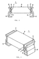
- FIGS. 1 and 2 illustrate a monolithic ceramic capacitor according to a first embodiment of the present invention.
- FIG. 1 is a front view
- FIG. 2 is a perspective view.
- the monolithic ceramic capacitor 1 contains a dielectric such as barium titanate type ceramic, and at the opposite end faces, external electrodes 2 are formed, respectively.
- the monolithic ceramic capacitor 1 is provided with a chip capacitor body 4 in which plural internal electrodes 3 (see FIG. 3 ) are formed in lamination so that each one is electrically connected to a predetermined one of the external electrodes 2, and is further provided with terminal members 6 each formed of a metal plate bonded to the external electrodes 2 by use of solder 5 as a conductive bonding material.
- each terminal member 6 has a protuberance 7 formed so as to project toward the external electrode 2, and the bonding portion 8 of the terminal member 6 bonded to the external electrode 2 by use of the solder 5 is formed so as to be elongated substantially linearly across a part of the external electrode 2.
- each bonding portion 8 as described above is elongated substantially linearly in parallel to the direction in which the internal electrodes 3 ( FIG. 3 ) are extended.
- the protuberance 7 for forming the bonding portion 8 which is elongated substantially linearly is also formed so as to be elongated continuously linearly. More concretely, the protuberance 7 is formed of a bending line provided in the metal plate constituting the terminal member 6.
- the bonding portion 8 is provided, for example, by forming a solder film on the external electrode 2 previously, and melting the solder film while the terminal member 6 is in contact with the solder film, whereby the bonding portion 8 is formed so as to have a fillet generated by the shrinkage of the solder caused by the surface tension.
- the bonding portion 8 does not go all the way across the external electrode 2. That is, the size of the bonding portion 8 in the longitudinal direction (the size in the direction perpendicular to the plane of FIG. 1 ) is shorter than the size of the end-face of the capacitor body 4 in the same direction (the size in the direction perpendicular to the plane of FIG. 1 ). This is one of measures which relax as much as possible the thermal shock that is generated during soldering with solder 5.
- FIG. 3 illustrates the displacement distribution between a pair of internal electrodes 3 which is caused by electrostriction.
- FIG. 4 is an enlarged view of part of the monolithic ceramic capacitor 1 of FIG. 1 .
- the displacement caused by the electrostriction increases with distance from the center line C 1 between a pair of the internal electrodes 3. Therefore, considering the whole of the capacitor body 4 in which plural layers of such internal electrodes 3 are laminated, the displacement most likely to be caused by the electrostriction is displacement in a thickness mode, as indicated by arrow 9 in FIG. 4 .
- the bonding portion 8 of the terminal member 6 and the external electrode 2 lies along only a limited part of the external electrode 2, and is elongated substantially linearly in parallel to the direction in which the internal electrodes 3 are extended. Therefore, the displacement in a thickness mode caused by the electrostriction as described above, not constrained substantially by the terminal member 6, is transmitted to both the main faces 10 of the capacitor body 4, and the energy of such displacement is effectively emitted from both the main faces 10 which are free ends of the capacitor body 4, as indicated by arrow 11.
- the protuberance 7 of the terminal member 6 is disposed as near to the center line C in the thickness direction of the capacitor body 4 as possible, as shown in FIG.4 , and the center in the width direction of the bonding portion 8 formed of the solder 5 is positioned as near to the center line C as possible.
- the distance a between the center in the width direction of the bonding portion 8 and one-side edge of the end-face of the capacitor body 4 in the lamination direction (the thickness direction of the capacitor body 4) of the internal electrodes 3 is in the range of preferably 1/5 to 4/5, more preferably 2/8 to 6/8, and most preferably 3/8 to 5/8 of the size b of the end face of the capacitor body 4, the size b being measured in the lamination direction of the internal electrodes 3.
- the width c of the bonding portion 8 is as short as possible.
- the width c of the bonding portion 8 is selected to be preferably up to 2/3, more preferably up to 4/9, still more preferably up to 1/3 of the size b of the end-face of the capacitor body 4, the size being measured in the lamination direction of the internal electrodes 3.
- FIGS. 5 , 6, 7, and 8 are partial front views showing monolithic ceramic capacitors 1a, 1b, 1c, and 1d according to a second, a third, a fourth, and a fifth embodiment of the present invention, respectively. Elements shown in FIGS. 5 through 8 equivalent to those in FIG. 1 are designated by similar reference numerals. Duplicated description is omitted.
- a protuberance 7 is formed by the tip of a bent-portion of a terminal member 6a.
- a protuberance 7 is formed by a C-shaped bent-portion of a terminal member 6b.
- a protuberance 7 is formed by part of a loop-shaped bent-portion of a terminal member 6c.
- the protuberance 7 of a terminal member 6d is not so sharp as that in FIG. 1 but has a predetermined width.
- FIGS. 9, 10 , and 11 illustrate monolithic ceramic capacitors 1e, 1f, and 1g according to a sixth, a seventh, and an eighth embodiment of the present invention, respectively.
- FIGS. 9 and 10 are front views
- FIG. 11 is a perspective view. Elements shown in FIGS. 9 through 11 equivalent to those in FIG. 1 are designated by similar reference numerals. Duplicated description is omitted.
- a monolithic ceramic capacitor 1e as shown in FIG. 9 has a stack component structure in which plural, e.g., two capacitor bodies 4 are stacked and mounted together by terminal members 6e which are attached to the respective external electrodes 2 of the two capacitor bodies 4 in common. With these terminal members 6e, the two capacitor bodies 4 are electrically connected in parallel.
- the terminal members 6e have protuberances 7 formed correspondingly to the external electrodes 2.
- a gap 12 is provided between the two capacitor bodies 4 in order to prevent the electrostriction phenomena occurring in the respective capacitor bodies 4 from interfering with each other.
- the two capacitor bodies 4 may be bonded to each other by use of an adhesive such as an adhesive with a Shore A hardness of up to 90 which is capable of absorbing the electrostriction phenomenon, instead of the gap 12.
- a monolithic ceramic capacitor 1f as shown in FIG. 10 is provided with plural, e.g., two capacitor bodies 4 which are arranged in series so as to lie in a plane.
- the external electrodes 2 of the respective two capacitor bodies 4 to be connected to each other are bonded by use of a conductive bonding material such as solder or a conductive adhesive.
- An appropriate terminal member preferably having a protuberance, though not illustrated, may be inserted between the external electrodes 2 and bonded with the conductive bonding material, if necessary.
- Terminal members 6f are attached to the external electrodes 2 positioned at opposite ends of the two capacitor bodies 4 electrically connected in series, respectively.
- the terminal members 6f have substantially the same shape as the terminal members 6 as shown in FIG. 1 .
- a monolithic ceramic capacitor 1g as shown in FIG. 11 is provided with plural, e.g., two capacitor bodies 4, which are arranged in parallel so as to lie in a plane. These two capacitor bodies 4 are bonded by use of a two-sided pressure-sensitive adhesive tape or an adhesive.
- Terminal members 6g each have such a length that the respective external electrodes 2 of the two capacitor bodies 4 can be connected in common.
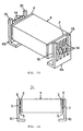
- FIG. 12 is a front view of a monolithic ceramic capacitor 1h according to a ninth embodiment of the present invention, in which a part of the monolithic ceramic capacitor is illustrated in a cross section. Elements in FIG. 12 equivalent to those in FIG. 1 are designated by similar reference numerals, and the duplicated description is omitted.
- the monolithic ceramic capacitor 1h of FIG. 12 is provided with a case 13 for accommodating a capacitor body 4 while terminal members 6h partially project outside.
- a case 13 for accommodating a capacitor body 4 while terminal members 6h partially project outside.
- FIG. 13 In the perspective view of FIG. 13 , only the components which are accommodated in the case 13 of the monolithic ceramic capacitor 1h are illustrated.
- the terminal members 6h each are provided with plural, e.g., three comb-teeth shape pieces 14.
- Protuberances 7 are formed in the comb-teeth shape pieces 14, respectively. That is, in this embodiment, the plural protuberances 7 are formed in each terminal member 6h so as to be distributed substantially linearly.
- positioning pieces 15 are integrally formed at both sides of the terminal member 6h.
- the positioning pieces 15 are provided to position the capacitor body 4 in the case 13, as seen most clearly in FIG. 12 .
- the capacitor body 4 is covered with the case 13. Therefore, the transmission of impact to the capacitor body 4 produced during mounting can be reduced, and moreover, breaking of the capacitor body 4 caused by collision with external objects can be prevented. In addition, an undesired stress applied to the terminal member 6h can be prevented from being propagated to the bonding portion 8.
- the space inside the case 13 may be packed with an appropriate resin (potting material).
- potting material By this means, the inside of the case 13 is shielded from moisture, gases, and so forth, and further improvements in reliability are realizable.
- heat is generated due to the impedance of the capacitor body 4.
- a potting resin having a high thermal conductivity the heat radiation efficiency can be enhanced, as compared with the instance where a space remains in the case 13.
- FIG. 14 is a front view of a monolithic ceramic capacitor 1i according to a tenth embodiment of the present invention. Elements in FIG. 14 equivalent to those in FIG. 1 are designated by similar reference numerals, and duplicated description is omitted.
- the monolithic ceramic capacitor 1i as shown in FIG. 14 is provided with terminal members 6i only one of which is shown in FIG. 15.
- FIG. 15 illustrates the side of the terminal member 6i which faces the external electrode 2.
- the terminal member 6i is provided with plural protuberances 7 distributed substantially linearly. These protuberances 7 can be formed by deep drawing by means of a press when the terminal member 6i is shaped.
- the bonding portion 8 for bonding to an external electrode 2, formed of a solder 5 can be distributed substantially linearly across a part of the external electrode 2.
- the solder 5 is used as the conductive bonding material for bonding the terminal members 6 or the like to the external electrodes 2.
- a conductive adhesive may be employed instead of the solder 5.
- the advantages of the present invention become more prominent by using solder having a relatively high hardness such as lead-free solder.
- the bonding portion 8 is formed so as to be elongated linearly along one straight line.
- the bonding portion 8 may be formed so as to be elongated along at least two straight lines or along a curved line.
- solder may be applied to other areas of the terminal members 6 or the like, and the external electrodes 2, in other places besides the bonding portion 8.
- solder may be coated all over the surface of an external electrode 2 or a terminal member 6.
- the structure containing the case 13 as shown in FIG. 12 may be employed in the respective embodiments as shown in FIGS. 1 , 5 through 11 , and 14 .
- the shapes of the terminal members as shown in FIG. 5 through 8 , 12 , and 14 may be employed.
- the terminal members 6h as shown in FIG. 12 may be applied to a monolithic ceramic capacitor not provided with the case 13.
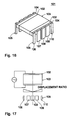
- FIG. 16 is a perspective view of a monolithic ceramic capacitor 101 according to an eleventh embodiment of the present invention.
- the monolithic ceramic capacitor 101 is provided with external electrodes 102 formed at the opposite end faces thereof, a chip capacitor body 103 in which plural internal electrodes (not illustrated) are formed in lamination so as to be electrically connected to a predetermined one of the external electrodes 102, respectively, and terminal members 105 each formed of a metal plate bonded to the external electrodes 102 by use of solder 104 as a conductive bonding material.
- each terminal member 105 comprises plural, e.g., five terminal elements 106, 107, 108, 109, and 110 arranged so as to be distributed at intervals in the width direction of the external electrode 2.
- These terminal elements 106 through 110 are so constructed that the terminal elements 106 and 110 positioned at the ends in the arrangement direction have a lower constraining-degree than the terminal element 108 or the terminal elements 107 through 109 positioned in the center, said constraining degree being defined as the degree of constraining a stress produced by the electrostriction phenomenon in the capacitor body 103, which is attributed to the bonding of the terminal elements 106 through 110 to the external electrode 102.
- the terminal elements positioned at the ends in the arrangement direction have a smaller bonding area on the external electrode 102, as compared with the terminal elements positioned in the center. Still more concretely, as compared with the terminal elements 108 or the terminal elements 107 through 109 positioned in the center, the terminal elements 106 and 110 positioned at the ends in the arrangement direction have a smaller size in the width direction, and moreover, the intervals between the terminal elements 106 and 110 and the corresponding next terminal elements 107 and 109 are wider than those between the terminal element 108 at the center and the next terminal elements 107 and 109.
- FIG. 17 shows the position relationship of the terminal elements 106 through 110 to the capacitor body 103 in the width direction of the external electrode 102.
- illustrated is the displacement distribution in the width direction of the external electrode 102 of the capacitor body 103 caused by electrostriction.
- the displacement ratio of the capacitor body 103 When the electrostriction in an area mode is generated in the monolithic ceramic capacitor 101, the displacement ratio of the capacitor body 103, observed in the width direction of the external electrode 102, is zero at the center, and becomes larger at a position farther from the center, as shown in FIG. 17 .
- the terminal elements 106 and 110 positioned at the ends where a high displacement ratio is caused by the electrostriction can be adjusted to have a lower constraining-degree than those of the terminal elements 108 or the terminal elements 107 through 109 positioned in the center where a low displacement ratio is caused by the electrostriction by setting the size in the width direction of the terminal elements 106 and 110 positioned at the ends to be smaller than that of the terminal element 108 or 107 through 109 positioned in the center, and moreover, setting the intervals between the terminal elements 106 and 110 positioned at the ends and the corresponding next terminal elements 107 and 109 to be wider than those between the terminal element 108 positioned at the center and the next terminal elements 107 and 109.
- the above-described embodiment can reduce the degree of constraint of a stress produced by the electrostriction phenomenon in the capacitor body 103, which is attributed to the bonding of the terminal elements 106 through 110 to the external electrode 102.
- Two means are employed for reducing the constraining-degree of the terminal elements positioned at the ends in the arrangement direction of the plural terminal elements 106 through 110, to be lower than that of the terminal elements positioned in the center; first, changing the sizes in the width direction of the terminal elements 106 through 110, and second, changing the intervals between the terminal elements 106 through 110. Either one or both of these two means may be employed. This will be described below with reference to FIGS. 18 and 19 .
- FIG. 18 given to explain changing the sizes in the width direction of the terminal elements, illustrates the positional relationship between the external electrode 112 on the capacitor body 111 and the terminal elements 113 and 114.
- the size in the width direction of the terminal element 113 positioned at the end is designated by W1, and that of the terminal element 114 positioned at the center by W2. All of the intervals between adjacent terminal elements of the plural terminal elements containing the terminal elements 113 and 114 are assumed to be equal, though not illustrated.
- the crack generation ratio is a ratio at which cracks are generated in the capacitor body 111 when a high frequency current is applied.
- the crack generation ratio can be reduced by setting the size W1 in the width direction of the terminal element 113 positioned at the end to be smaller than the size W2 in the width direction of the terminal element 114 at the center.
- the generation of cracks can be reliably prevented by setting the size W1 in the width direction to be smaller than the size W2 in the width direction multiplied by 0.8.
- FIG. 19 is a side view illustrating the positional relationship between the external electrode 112 on the capacitor body 111 and the terminal elements 115 through 118.
- the crack generation ratio can be reduced by setting the interval G1 between the terminal element 115 positioned at the end and the terminal element 116 to be wider than the interval G2 between the terminal element 117 positioned at the center and the terminal element 118.
- the generation of cracks can be reliably prevented by setting the interval G1 to be more than the interval G2 multiplied by 1.2.
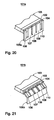
- FIGS. 20 and 21 are perspective views partially illustrating monolithic ceramic capacitors 101a and 101b according to twelfth and thirteenth embodiments of the present invention, respectively. Elements in FIGS. 20 and 21 equivalent to elements shown in FIG. 16 are designated by similar reference numerals. Duplicated description is omitted.
- each terminal member 105 of FIG. 16 the plural terminal elements 106 through 110 are independent of each other.
- the plural terminal elements 106 through 110 are formed in a comb-teeth shape.
- the terminal elements 106 through 110 each have a bending shape to form a line-shaped or point-shaped bonding portion on the external electrode 102.
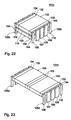
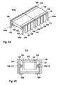
- FIGS. 22, 23 , and 24 are perspective views showing monolithic ceramic capacitors 101c, 101d, and 101e according to a fourteenth, a fifteenth, and a sixteenth embodiment of the present invention, respectively. Elements in FIGS. 22 through 24 equivalent to those in FIG. 16 are designated by similar reference numerals. Duplicated description is omitted.
- the monolithic ceramic capacitor 101c as shown in FIG. 22 has a stack component shape in which plural, e.g., two capacitor bodies 103 are stacked and attached together by a terminal member 105c comprising plural terminal elements 106 through 110 which is attached to the respective external electrodes 102 of the two capacitor bodies 103 in common. With the terminal members 105c, the two capacitor bodies 103 are electrically connected in parallel.
- a gap 119 is provided between the two capacitor bodies 103 to prevent the electrostriction phenomena occurring in the respective capacitor bodies 103 from interfering with each other.
- the two capacitor bodies 103 may alternatively be bonded to each other through an adhesive with a Shore A hardness of up to 90 instead of the gap 119.
- the monolithic ceramic capacitor 101d as shown in FIG. 23 is provided with plural, e.g., two capacitor bodies 103. These capacitor bodies 103 are arranged in series so as to lie in a plane.
- the external electrodes 102 to be connected of the two capacitor bodies 103 are bonded to each other through a conductive bonding material such as solder, a conductive adhesive, or the like.
- An appropriate terminal member, though not illustrated, may be inserted between the external electrodes 102 and bonded through the conductive bonding material, if necessarily.
- Terminal members 105d composed of plural terminal elements 106 through 110 are attached to the external electrodes 102 positioned at the opposite ends of the two capacitor bodies 103 electrically connected in series as described above, respectively.
- the monolithic ceramic capacitor 101e as shown in FIG. 24 is provided with plural, e.g., two capacitor bodies 103. These capacitor bodies 103 are arranged in an array component form in which the capacitor bodies 103 are arranged in parallel so as to lie in a plane and connected together. These two capacitor bodies 103 are bonded to each other by use of a two-side pressure-sensitive tape or an adhesive.
- Terminal members 105e each composed of plural terminal elements 106 through 110 are attached to the external electrodes 102 of the two capacitor bodies 103, respectively.
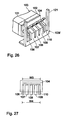
- FIG. 25 is a sectional, front partial view showing a monolithic ceramic capacitor 101f according to a seventeenth embodiment of the present invention. Elements in FIG. 25 equivalent to those in FIG. 16 are designated by similar reference numerals. Duplicated description is omitted.
- the monolithic ceramic capacitor 101f as shown in FIG. 25 is provided with a case 120 for accommodating a capacitor body 103 while terminal members 105f are partially exposed outside.
- the perspective view of FIG. 26 is only a partial view of the components accommodated in the case 120 of the monolithic ceramic capacitor 101f.
- each terminal member 105f plural terminal elements 106 through 110 are formed in a comb-teeth shape similarly to the terminal member 105b as shown in FIG. 21 , and moreover, the terminal elements 106 through 110 are bent, respectively.
- positioning pieces 121 are integrally provided for each terminal member 105f at both sides thereof The positioning pieces 121 are provided to position the capacitor body 103 in the case 120, as seen most clearly in FIG. 25 .
- the capacitor body 103 is covered with the case 120.
- the transmission of impact during mounting to the capacitor body 103 can be reduced, and moreover, breaking of the capacitor body 103 caused by collision with external objects can be prevented.
- the case 120 can prevent an undesired stress applied to the terminal member 1 05f from being propagated to the bonding portion formed with solder 104.
- the space inside the case 120 may be packed with an appropriate resin (potting resin).
- potting resin By this way, the inside of the case 120 is shielded from moisture, gases, and so forth, and further improvements in reliability are realizable.
- high voltage or high frequency current is applied to the monolithic ceramic capacitor 101f, heat is generated due to the impedance of the capacitor body 103.
- a resin having a high thermal conductivity is employed as a potting resin, the heat radiating efficiency can be enhanced, as compared with the instance where the space remains in the case 120.
- the solder 104 is used as the conductive bonding material for bonding the terminal members 105 or the like to the external electrodes 102.
- conductive adhesive may be employed.
- the solder 104 is coated all over the surface of the external electrodes 102.
- the solder 104 may be applied only to the portion required for the bonding to the terminal members 105 or the like.
- the overall size in the width direction of the respective terminal elements 106 and 110 is decreased.
- a notch or the like may be provided to reduce the size in the width direction.
- the bonding areas of the plural terminal elements 106 through 110 bonded to the external electrode 102 effects of a stress caused by the electrostriction are reduced by making the bonding areas of the terminal elements at the ends in the width direction of the external electrode 102 smaller than those of the terminal elements in the center.
- the thickness of the terminal elements positioned at the ends in the arrangement direction may be thinner than that of the terminal elements positioned in the center so that the degree of constraining a stress caused by the electrostriction is reduced.
- terminal members each bonded to an external electrode of a capacitor body through a conductive bonding material are provided with a protrusion projecting toward the external electrode, and thereby, the bonding portion of the terminal member bonded to the external electrode, formed with the conductive bonding material is elongated substantially linearly on a part of the external electrode. Accordingly, electrostriction phenomena in the capacitor body are scarcely constrained, so that a stress caused by the electrostriction can be relaxed. Accordingly, breaking of the bonding portion and cracking of the capacitor body, and so forth, caused by such a stress, can be advantageously prevented. In addition, "creaking" can be considerably reduced.
- the width of the bonding portion is selected to be preferably up to 2/3, more preferably up to 4/9, and most preferably up to 1/3 of the size of the end face of the capacitor body, the size being measured in the lamination direction of the internal electrodes, the effect on the relaxation of a stress generated by electrostriction as described above can be achieved more securely.
- the center in the width direction of the bonding portion is positioned in the range of 1/5 to 4/5, more preferably 2/8 to 6/8, and still more preferably 3/8 to 5/8 of the size of the end face from one side edge of the end face of the capacitor body in the lamination direction of the internal electrodes, the size being measured in the lamination direction of the internal electrodes, the effect on the relaxation of a stress generated by the electrostriction can be achieved more reliably as in the above instance.
- the terminal members when the structure is employed in which plural capacitor bodies are provided, and terminal members are attached to the respective external electrodes of the capacitor bodies in common, the terminal members can function as a conductive member for connecting the plural capacitor bodies in parallel, for example. Accordingly, for example, a stack component can be simply obtained.
- the capacitor body can be easily positioned without addition of a special piece for positioning, assembly of the monolithic ceramic capacitor can be simply carried out, and breaking of the monolithic ceramic capacitor in the mounting state can be advantageously prevented.
- a terminal member is provided with plural terminal elements arranged so as to be distributed at intervals in the width direction of an external electrode.
- the plural terminal elements are constructed so that as to set the degree of constraining a stress produced by the electrostriction phenomenon in a capacitor body, which is attributed to the bonding of the terminal elements to the external electrode. More specifically, each terminal element positioned at the ends in the arrangement direction has a lower constraining-degree than each terminal element positioned in the center. Accordingly, on the portions where the terminal members are bonded to the external electrodes, on the capacitor body, and so forth, effects of a stress caused by electrostriction can be reduced. As a result, breaking of the bonding portions and cracking in the capacitor body, and so forth can be advantageously prevented.
- the desired degree of constraint can be simply realized, by setting the plural terminal elements at the ends in the width direction of the external electrode so as to have a smaller bonding area on the external electrode, as compared with the bonding area in the center.
- the degree of constraining a stress as described above can be desirably realized by a simpler method by setting the plural terminal elements so that the size in the width direction of each terminal element positioned at the ends in the arrangement direction is smaller than each terminal element positioned in the center, and/or by setting the plural terminal elements so that the intervals between the terminal elements positioned at the ends in the arrangement direction and the next terminal elements are longer than those between the terminal element positioned in the center and the next terminal elements.
- the plural terminal elements may have the form that they are independent of each other or the terminal members each may have the plural terminal elements formed in a comb-teeth shape.
- These plural terminal elements can be simply obtained by changing suitably the cutting position of a material, for example, a hoop material, prepared for production of the terminal members.
- the capacitor body can be easily positioned without addition of a special piece for positioning, assembly of the monolithic ceramic capacitor can be easily carried out, and breaking of the monolithic ceramic capacitor in the mounting state can be advantageously prevented.
Landscapes
- Engineering & Computer Science (AREA)
- Power Engineering (AREA)
- Manufacturing & Machinery (AREA)
- Microelectronics & Electronic Packaging (AREA)
- Ceramic Capacitors (AREA)
- Fixed Capacitors And Capacitor Manufacturing Machines (AREA)
Applications Claiming Priority (4)
| Application Number | Priority Date | Filing Date | Title |
|---|---|---|---|
| JP35585098 | 1998-12-15 | ||
| JP36049998A JP3307351B2 (ja) | 1998-12-18 | 1998-12-18 | 積層セラミックコンデンサ |
| JP02971999A JP3687832B2 (ja) | 1998-12-15 | 1999-02-08 | 積層セラミックコンデンサ |
| EP99125047A EP1011117A3 (de) | 1998-12-15 | 1999-12-15 | Monolithischer keramischer kondensator |
Related Parent Applications (2)
| Application Number | Title | Priority Date | Filing Date |
|---|---|---|---|
| EP99125047A Division EP1011117A3 (de) | 1998-12-15 | 1999-12-15 | Monolithischer keramischer kondensator |
| EP99125047.3 Division | 1999-12-15 |
Publications (2)
| Publication Number | Publication Date |
|---|---|
| EP1950775A1 true EP1950775A1 (de) | 2008-07-30 |
| EP1950775B1 EP1950775B1 (de) | 2013-07-03 |
Family
ID=27286696
Family Applications (2)
| Application Number | Title | Priority Date | Filing Date |
|---|---|---|---|
| EP99125047A Withdrawn EP1011117A3 (de) | 1998-12-15 | 1999-12-15 | Monolithischer keramischer kondensator |
| EP08008922.0A Expired - Lifetime EP1950775B1 (de) | 1998-12-15 | 1999-12-15 | Monolithischer keramischer Kondensator |
Family Applications Before (1)
| Application Number | Title | Priority Date | Filing Date |
|---|---|---|---|
| EP99125047A Withdrawn EP1011117A3 (de) | 1998-12-15 | 1999-12-15 | Monolithischer keramischer kondensator |
Country Status (2)
| Country | Link |
|---|---|
| US (2) | US6574089B1 (de) |
| EP (2) | EP1011117A3 (de) |
Cited By (1)
| Publication number | Priority date | Publication date | Assignee | Title |
|---|---|---|---|---|
| DE102018104459A1 (de) * | 2018-02-27 | 2019-08-29 | Tdk Electronics Ag | Vielschichtbauelement mit externer Kontaktierung |
Families Citing this family (35)
| Publication number | Priority date | Publication date | Assignee | Title |
|---|---|---|---|---|
| JP3883528B2 (ja) * | 2003-08-19 | 2007-02-21 | Tdk株式会社 | 電子部品 |
| US20080030922A1 (en) * | 2004-09-27 | 2008-02-07 | Matsushita Electric Industrial Co., Ltd. | Multi-Layer Capacitor and Mold Capacitor |
| EP1890302B1 (de) * | 2005-05-23 | 2018-06-20 | Murata Manufacturing Co., Ltd. | Keramik-elektronikkomponente und verfahren zu deren herstellung |
| JP2007220751A (ja) * | 2006-02-14 | 2007-08-30 | Tdk Corp | セラミックコンデンサの実装構造及びセラミックコンデンサ |
| US20080012127A1 (en) * | 2006-06-28 | 2008-01-17 | Inpaq Technology Co., Ltd. | Insulation structure for multilayer passive elements and fabrication method thereof |
| US20080036556A1 (en) * | 2006-08-10 | 2008-02-14 | Honeywell International Inc. | Methods and apparatus for installing a feed through filter |
| TWI303543B (en) * | 2006-10-16 | 2008-11-21 | Delta Electronics Inc | Stacked electronic device and the clipping device thereof |
| CN101170012B (zh) * | 2006-10-24 | 2010-06-09 | 台达电子工业股份有限公司 | 堆叠式电子元件及其夹持组件 |
| JP5045649B2 (ja) * | 2008-11-17 | 2012-10-10 | 株式会社村田製作所 | セラミックコンデンサ及びそれを備えた電子部品 |
| JP4867999B2 (ja) * | 2009-01-20 | 2012-02-01 | Tdk株式会社 | 積層コンデンサ |
| JP5035318B2 (ja) * | 2009-10-23 | 2012-09-26 | Tdk株式会社 | 積層型コンデンサ |
| JP5857847B2 (ja) * | 2011-06-22 | 2016-02-10 | 株式会社村田製作所 | セラミック電子部品 |
| JP5154676B2 (ja) * | 2011-06-29 | 2013-02-27 | 双信電機株式会社 | コンデンサ |
| DE102011107193A1 (de) * | 2011-07-13 | 2013-01-17 | Epcos Ag | Elektrische Vorrichtung |
| KR101420517B1 (ko) * | 2012-10-31 | 2014-07-16 | 삼성전기주식회사 | 적층 세라믹 캐패시터 및 이를 포함하는 인쇄회로기판 |
| US10229785B2 (en) * | 2012-12-06 | 2019-03-12 | Kemet Electronics Corporation | Multi-layered ceramic capacitor with soft leaded module |
| WO2015065974A1 (en) * | 2013-10-29 | 2015-05-07 | Kemet Electronics Corporation | Ceramic capacitors with improved lead designs |
| DE102015017344B3 (de) | 2015-02-27 | 2024-10-24 | Tdk Electronics Ag | Keramisches Bauelement, Bauelementanordnung und Verfahren zur Herstellung eines keramischen Bauelemements |
| DE102015102866B4 (de) * | 2015-02-27 | 2023-02-02 | Tdk Electronics Ag | Keramisches Bauelement, Bauelementanordnung und Verfahren zur Herstellung eines keramischen Bauelements |
| JP6477234B2 (ja) | 2015-05-20 | 2019-03-06 | Tdk株式会社 | 電子部品 |
| JP6520398B2 (ja) | 2015-05-27 | 2019-05-29 | Tdk株式会社 | 電子部品 |
| JP6776582B2 (ja) * | 2016-03-31 | 2020-10-28 | Tdk株式会社 | 電子部品 |
| JP6828432B2 (ja) * | 2016-12-28 | 2021-02-10 | Tdk株式会社 | セラミック電子部品 |
| US10507377B2 (en) * | 2017-05-02 | 2019-12-17 | Dean L. Sicking | Sports wall assembly |
| US11195663B2 (en) | 2017-05-12 | 2021-12-07 | Amrad Manufacturing, Llc | Capacitor with multiple elements for multiple replacement applications |
| CN109065437B (zh) * | 2018-08-03 | 2020-04-24 | 北京理工大学 | 一种四极电场联合偶极电场的离子共振激发操作方法和装置 |
| KR102211743B1 (ko) * | 2018-08-29 | 2021-02-03 | 삼성전기주식회사 | 전자 부품 |
| KR102142517B1 (ko) * | 2018-09-04 | 2020-08-07 | 삼성전기주식회사 | 전자 부품 |
| USD906969S1 (en) * | 2018-12-13 | 2021-01-05 | American Radionic Company, Inc. | Magnet for attachment to a capacitor |
| KR102341635B1 (ko) * | 2018-12-25 | 2021-12-22 | 티디케이가부시기가이샤 | 전자 부품 |
| CN110211755A (zh) * | 2019-05-31 | 2019-09-06 | 国网湖南省电力有限公司 | 笼式避雷器绝缘筒和防爆避雷器 |
| JP7319133B2 (ja) * | 2019-07-31 | 2023-08-01 | 太陽誘電株式会社 | 積層セラミック電子部品及び電子部品実装基板 |
| JP7428962B2 (ja) * | 2019-10-28 | 2024-02-07 | Tdk株式会社 | セラミック電子部品 |
| KR102825915B1 (ko) * | 2020-09-09 | 2025-06-27 | 삼성전기주식회사 | 전자 부품 및 그 실장 기판 |
| CN115985688A (zh) * | 2021-10-15 | 2023-04-18 | 惠州精勤电子元件有限公司 | 一种多芯片并联贴片x电容器 |
Citations (6)
| Publication number | Priority date | Publication date | Assignee | Title |
|---|---|---|---|---|
| US4320281A (en) | 1980-07-31 | 1982-03-16 | Western Electric Company, Inc. | Laser bonding technique and article formed thereby |
| US4617609A (en) | 1984-04-03 | 1986-10-14 | Siemens Aktiengesellschaft | Electric capacitor in the form of a chip component and method for manufacturing same |
| US4715118A (en) | 1985-05-10 | 1987-12-29 | Compagnie Europeene De Composants Electroniques | Connecting strip for the manufacture of direct transfer electric components and manufacturing method for such components |
| US4777558A (en) | 1986-10-23 | 1988-10-11 | Marcon Electronics Co., Ltd. | Electronic device |
| US5196986A (en) * | 1992-04-21 | 1993-03-23 | Vim Electronic Co., Ltd. | Capacitor |
| JPH0722274A (ja) | 1993-07-05 | 1995-01-24 | Murata Mfg Co Ltd | チップ型電子部品 |
Family Cites Families (11)
| Publication number | Priority date | Publication date | Assignee | Title |
|---|---|---|---|---|
| JPS5322738A (en) | 1976-08-16 | 1978-03-02 | Yashica Co Ltd | Circuit for deciding time constant capacitor charging time of electric shutter |
| JPS6240818A (ja) | 1985-08-19 | 1987-02-21 | Fujitsu Ltd | スイツチ回路 |
| JPH03225810A (ja) * | 1990-01-30 | 1991-10-04 | Rohm Co Ltd | 積層型コンデンサーにおける端子電極膜の構造及び端子電極膜の形成方法 |
| JPH0497304A (ja) | 1990-08-16 | 1992-03-30 | Fuji Photo Film Co Ltd | 放射線画像読取装置 |
| JP2900596B2 (ja) * | 1990-11-22 | 1999-06-02 | 三菱マテリアル株式会社 | 複合セラミックコンデンサ |
| JPH0543503A (ja) | 1991-08-15 | 1993-02-23 | Seimi Chem Kk | トラン誘導体化合物、液晶組成物及び液晶電気光学素子 |
| JP3365426B2 (ja) * | 1992-10-06 | 2003-01-14 | 日本ケミコン株式会社 | チップ型電子部品 |
| US6191933B1 (en) * | 1998-01-07 | 2001-02-20 | Tdk Corporation | Ceramic capacitor |
| JP3520776B2 (ja) * | 1998-05-28 | 2004-04-19 | 株式会社村田製作所 | 電子部品 |
| JP3477692B2 (ja) * | 1998-12-18 | 2003-12-10 | 株式会社村田製作所 | 電子部品 |
| JP2000235932A (ja) * | 1999-02-16 | 2000-08-29 | Murata Mfg Co Ltd | セラミック電子部品 |
-
1999
- 1999-12-15 US US09/464,236 patent/US6574089B1/en not_active Expired - Lifetime
- 1999-12-15 EP EP99125047A patent/EP1011117A3/de not_active Withdrawn
- 1999-12-15 EP EP08008922.0A patent/EP1950775B1/de not_active Expired - Lifetime
-
2002
- 2002-07-26 US US10/207,406 patent/US6661641B2/en not_active Expired - Lifetime
Patent Citations (6)
| Publication number | Priority date | Publication date | Assignee | Title |
|---|---|---|---|---|
| US4320281A (en) | 1980-07-31 | 1982-03-16 | Western Electric Company, Inc. | Laser bonding technique and article formed thereby |
| US4617609A (en) | 1984-04-03 | 1986-10-14 | Siemens Aktiengesellschaft | Electric capacitor in the form of a chip component and method for manufacturing same |
| US4715118A (en) | 1985-05-10 | 1987-12-29 | Compagnie Europeene De Composants Electroniques | Connecting strip for the manufacture of direct transfer electric components and manufacturing method for such components |
| US4777558A (en) | 1986-10-23 | 1988-10-11 | Marcon Electronics Co., Ltd. | Electronic device |
| US5196986A (en) * | 1992-04-21 | 1993-03-23 | Vim Electronic Co., Ltd. | Capacitor |
| JPH0722274A (ja) | 1993-07-05 | 1995-01-24 | Murata Mfg Co Ltd | チップ型電子部品 |
Cited By (2)
| Publication number | Priority date | Publication date | Assignee | Title |
|---|---|---|---|---|
| DE102018104459A1 (de) * | 2018-02-27 | 2019-08-29 | Tdk Electronics Ag | Vielschichtbauelement mit externer Kontaktierung |
| US11387045B2 (en) | 2018-02-27 | 2022-07-12 | Tdk Electronics Ag | Multilayer component with external contact |
Also Published As
| Publication number | Publication date |
|---|---|
| EP1011117A3 (de) | 2004-11-10 |
| EP1011117A2 (de) | 2000-06-21 |
| US6661641B2 (en) | 2003-12-09 |
| EP1950775B1 (de) | 2013-07-03 |
| US6574089B1 (en) | 2003-06-03 |
| US20030011959A1 (en) | 2003-01-16 |
Similar Documents
| Publication | Publication Date | Title |
|---|---|---|
| EP1950775A1 (de) | Monolidthischer Keramischer Kondensator | |
| JP3687832B2 (ja) | 積層セラミックコンデンサ | |
| JP3520776B2 (ja) | 電子部品 | |
| JP2003257784A (ja) | 電子部品 | |
| JP2005064377A (ja) | 電子部品 | |
| JP2004273935A (ja) | セラミックコンデンサ、及び、その製造方法 | |
| US6333589B1 (en) | Laminated piezoelectric transformer and method for manufacturing the same | |
| EP0823782B1 (de) | Piezoelektrisches Bauelement | |
| US10818432B2 (en) | Electronic device | |
| JP3307351B2 (ja) | 積層セラミックコンデンサ | |
| JP3147793B2 (ja) | ラダー型フィルタ | |
| US6362948B1 (en) | Electronic component | |
| JP2000223357A (ja) | 積層セラミックコンデンサ | |
| US10796854B2 (en) | Electronic device | |
| JP2023001300A (ja) | セラミック電子部品 | |
| US10763043B2 (en) | Electronic device | |
| JP3468043B2 (ja) | 積層圧電体トランス | |
| JPH0766313A (ja) | 複合電子部品 | |
| JP2003257779A (ja) | 電子部品 | |
| JP2002026467A (ja) | 電子回路基板 | |
| JPH10154835A (ja) | 圧電トランス | |
| JPH10284809A (ja) | 回路モジュール及びその製造方法 | |
| JPS6242523Y2 (de) | ||
| JPH08107259A (ja) | 表面実装用電子部品 | |
| JP2504142B2 (ja) | 圧電アクチュエ―タ |
Legal Events
| Date | Code | Title | Description |
|---|---|---|---|
| PUAI | Public reference made under article 153(3) epc to a published international application that has entered the european phase |
Free format text: ORIGINAL CODE: 0009012 |
|
| 17P | Request for examination filed |
Effective date: 20080514 |
|
| AC | Divisional application: reference to earlier application |
Ref document number: 1011117 Country of ref document: EP Kind code of ref document: P |
|
| AK | Designated contracting states |
Kind code of ref document: A1 Designated state(s): DE FR GB IT |
|
| 17Q | First examination report despatched |
Effective date: 20080918 |
|
| AKX | Designation fees paid |
Designated state(s): DE FR GB IT |
|
| GRAP | Despatch of communication of intention to grant a patent |
Free format text: ORIGINAL CODE: EPIDOSNIGR1 |
|
| RIC1 | Information provided on ipc code assigned before grant |
Ipc: H01G 4/232 20060101ALI20121210BHEP Ipc: H05K 3/34 20060101ALI20121210BHEP Ipc: H01G 4/228 20060101AFI20121210BHEP |
|
| GRAS | Grant fee paid |
Free format text: ORIGINAL CODE: EPIDOSNIGR3 |
|
| GRAA | (expected) grant |
Free format text: ORIGINAL CODE: 0009210 |
|
| AC | Divisional application: reference to earlier application |
Ref document number: 1011117 Country of ref document: EP Kind code of ref document: P |
|
| AK | Designated contracting states |
Kind code of ref document: B1 Designated state(s): DE FR GB IT |
|
| REG | Reference to a national code |
Ref country code: GB Ref legal event code: FG4D |
|
| REG | Reference to a national code |
Ref country code: DE Ref legal event code: R096 Ref document number: 69944816 Country of ref document: DE Effective date: 20130829 |
|
| PLBE | No opposition filed within time limit |
Free format text: ORIGINAL CODE: 0009261 |
|
| STAA | Information on the status of an ep patent application or granted ep patent |
Free format text: STATUS: NO OPPOSITION FILED WITHIN TIME LIMIT |
|
| PG25 | Lapsed in a contracting state [announced via postgrant information from national office to epo] |
Ref country code: IT Free format text: LAPSE BECAUSE OF FAILURE TO SUBMIT A TRANSLATION OF THE DESCRIPTION OR TO PAY THE FEE WITHIN THE PRESCRIBED TIME-LIMIT Effective date: 20130703 |
|
| 26N | No opposition filed |
Effective date: 20140404 |
|
| REG | Reference to a national code |
Ref country code: DE Ref legal event code: R097 Ref document number: 69944816 Country of ref document: DE Effective date: 20140404 |
|
| GBPC | Gb: european patent ceased through non-payment of renewal fee |
Effective date: 20131215 |
|
| REG | Reference to a national code |
Ref country code: FR Ref legal event code: ST Effective date: 20140829 |
|
| PG25 | Lapsed in a contracting state [announced via postgrant information from national office to epo] |
Ref country code: GB Free format text: LAPSE BECAUSE OF NON-PAYMENT OF DUE FEES Effective date: 20131215 Ref country code: FR Free format text: LAPSE BECAUSE OF NON-PAYMENT OF DUE FEES Effective date: 20131231 |
|
| PGFP | Annual fee paid to national office [announced via postgrant information from national office to epo] |
Ref country code: DE Payment date: 20181210 Year of fee payment: 20 |
|
| REG | Reference to a national code |
Ref country code: DE Ref legal event code: R071 Ref document number: 69944816 Country of ref document: DE |