EP1950778A2 - Procédé de contrôle de commande et unité pour dispositif de micro-machine - Google Patents
Procédé de contrôle de commande et unité pour dispositif de micro-machine Download PDFInfo
- Publication number
- EP1950778A2 EP1950778A2 EP08100445A EP08100445A EP1950778A2 EP 1950778 A2 EP1950778 A2 EP 1950778A2 EP 08100445 A EP08100445 A EP 08100445A EP 08100445 A EP08100445 A EP 08100445A EP 1950778 A2 EP1950778 A2 EP 1950778A2
- Authority
- EP
- European Patent Office
- Prior art keywords
- control voltage
- polarity
- variable capacitance
- electrodes
- micro machine
- Prior art date
- Legal status (The legal status is an assumption and is not a legal conclusion. Google has not performed a legal analysis and makes no representation as to the accuracy of the status listed.)
- Withdrawn
Links
Images






Classifications
-
- H—ELECTRICITY
- H01—ELECTRIC ELEMENTS
- H01H—ELECTRIC SWITCHES; RELAYS; SELECTORS; EMERGENCY PROTECTIVE DEVICES
- H01H59/00—Electrostatic relays; Electro-adhesion relays
- H01H59/0009—Electrostatic relays; Electro-adhesion relays making use of micromechanics
-
- B—PERFORMING OPERATIONS; TRANSPORTING
- B81—MICROSTRUCTURAL TECHNOLOGY
- B81B—MICROSTRUCTURAL DEVICES OR SYSTEMS, e.g. MICROMECHANICAL DEVICES
- B81B3/00—Devices comprising flexible or deformable elements, e.g. comprising elastic tongues or membranes
-
- H—ELECTRICITY
- H01—ELECTRIC ELEMENTS
- H01G—CAPACITORS; CAPACITORS, RECTIFIERS, DETECTORS, SWITCHING DEVICES, LIGHT-SENSITIVE OR TEMPERATURE-SENSITIVE DEVICES OF THE ELECTROLYTIC TYPE
- H01G5/00—Capacitors in which the capacitance is varied by mechanical means, e.g. by turning a shaft; Processes of their manufacture
- H01G5/16—Capacitors in which the capacitance is varied by mechanical means, e.g. by turning a shaft; Processes of their manufacture using variation of distance between electrodes
- H01G5/18—Capacitors in which the capacitance is varied by mechanical means, e.g. by turning a shaft; Processes of their manufacture using variation of distance between electrodes due to change in inclination, e.g. by flexing, by spiral wrapping
-
- H—ELECTRICITY
- H03—ELECTRONIC CIRCUITRY
- H03H—IMPEDANCE NETWORKS, e.g. RESONANT CIRCUITS; RESONATORS
- H03H7/00—Multiple-port networks comprising only passive electrical elements as network components
- H03H7/38—Impedance-matching networks
-
- H—ELECTRICITY
- H03—ELECTRONIC CIRCUITRY
- H03H—IMPEDANCE NETWORKS, e.g. RESONANT CIRCUITS; RESONATORS
- H03H7/00—Multiple-port networks comprising only passive electrical elements as network components
- H03H2007/006—MEMS
Definitions
- the present invention relates to a method and a unit for driving and controlling a micro machine device made up of first and second electrodes opposed to each other and a dielectric layer disposed between them, as well as a variable capacitance element and a variable capacitance switch using the method and the unit.
- micro machine processing technique also referred to as MEMS (Micro Electro Mechanical Systems) or MST (Micro System Technology)
- MEMS Micro Electro Mechanical Systems
- MST Micro System Technology
- the micro machine device can have functions of changing capacitance or electric switch by controlling a mechanical parameter. Therefore, electric characteristics such as a loss are hardly affected by the material, so it can obtain electrically good performances more easily than a switch or a variable capacitance device using a semiconductor.
- the micro machine device may also be called a "micro machining device", a “micro machine element”, a “MEMS electromechanical component” or the like.
- variable capacitance device variable capacitance element
- the variable capacitance device is made up of a substrate 21, a lower electrode 24, a dielectric film 26 covering the lower electrode 24, a supporting film 22 and an upper electrode 25 supported by the supporting film 22, which are formed on the substrate 21. There is a space KG between the dielectric film 26 and the upper electrode 25. Capacitance CP between the lower electrode 24 and the upper electrode 25 is changed by a displacement of the upper electrode 25.
- variable capacitance device can be hardly controlled substantially because variation of the capacitance CP with respect to the control voltage VC exhibits hysteresis so that reproducibility is too bad to obtain desired capacitance CP precisely.
- Fig. 4A shows variation of the capacitance CP when the control voltage VC is changed slowly. More specifically, the control voltage VC is increased slowly from 0 volt to 10 volts and then decreased to 0 volt, and it is further decreased to -10 volts and then increased to 0 volt. During this period hysteresis occurs, so the values of the capacitance CP at the same control voltage VC but on ascending timing and on descending timing are completely different. In addition, the capacitance CP at 0 volt of the control voltage VC is shifted to the larger side so that it has an offset value with respect to a natural value of the capacitance CP at 0 volt and cannot be reset. As a result, the capacitance CP at 0 volt of the control voltage VC is larger than the capacitance CP at 4 volts, for example.
- a method according to an aspect of the present invention is a drive control method for a micro machine device made up of first and second electrodes opposed to each other and a dielectric layer disposed between them.
- the drive control method includes the steps of applying a control voltage between the first and the second electrodes so that an electrostatic force is exerted on the first and the second electrodes for displacing the first or the second electrode, and switching polarity of the control voltage at a predetermined period or a shorter period.
- polarity of the control voltage is switched at a predetermined period or at a shorter period, for example switched at a period of time shorter than a certain specific period of time, it is possible to prevent charge up of the dielectric layer so that generation of hysteresis in capacitance can be suppressed. Note that if the switching is performed repeatedly, the periods (of time) may be different from each other.
- the period for switching the polarity of the control voltage is a short period of time in which polarization due to space charge transfer does not occur in the dielectric layer. For example, it is 100 milliseconds or shorter.
- an impedance matching circuit includes a variable capacitance element that is a micro machine device of variable capacitance having first and second electrodes opposed to each other and a dielectric layer disposed between them.
- a control voltage is applied between the first and the second electrodes so that an electrostatic force is exerted on the first and the second electrodes for displacing the first or the second electrode and thus matching impedance, and polarity of the control voltage is switched during an idle period of the communication circuit.
- variable capacitance variable capacitance element
- a transmission and reception switching circuit includes a first variable capacitance switch made up of a micro machine device that enables a transmission circuit to perform transmission operation when it is turned on, and a second variable capacitance switch made up of a micro machine device that enables a reception circuit to perform reception operation when it is turned on.
- Each of the first and the second variable capacitance switches includes first and second electrodes opposed to each other and a dielectric layer disposed between them. The first or the second electrodes are displaced so as to switch on and off of a circuit when a control voltage is applied between the first and the second electrodes. Polarity of the control voltage to be applied is switched at the timing of switching each of the first and the second variable capacitance switches from off to on.
- variable capacitance switch made up of a micro machine device, switching operation of transmission and reception can be performed securely with a simple structure.
- the present invention it is possible to suppress generation of hysteresis in the voltage control characteristic of the micro machine device including first and second electrodes opposed to each other and a dielectric layer disposed between them. Thus, it is possible to perform more accurate control more easily than the conventional method.
- a micro machine system 3 is made up of a variable capacitance device 11 that is a micro machine device and a driving circuit 12.
- the variable capacitance device (variable capacitance element) 11 includes a substrate 21 made of silicone, glass or the like, a lower electrode 24 formed on the substrate 21, and a dielectric film 26 covering the lower electrode 24.
- supporting films 22 and 23, and an upper electrode 25 supported by the supporting films 22 and 23 are also formed on the substrate 21.
- a space KG is provided between the dielectric film 26 and the upper electrode 25.
- the driving circuit 12 applies a control voltage VC between the lower electrode 24 and the upper electrode 25.
- electrostatic force electrostatic attraction
- the upper electrode 25 is attracted and displaced downward.
- the space KG is decreased so that a value of the capacitance CP increases.
- the driving circuit 12 is made up of an output voltage adjusting portion 33 and a polarity inverted signal S1 that is supplied externally.
- the driving circuit 12 can be realized by hardware using an analog or digital circuit element, or software using a CPU, a DSP or the like executing an appropriate program, or a combination of the both.
- the output voltage adjusting portion 33 adjusts the control voltage VC that is applied to the variable capacitance device 11 to be a predetermined value.
- a value of the control voltage VC is determined in accordance with a purpose and contents of the control.
- a polarity of the control voltage VC changes in accordance with the polarity inverted signal S1 supplied externally.
- the polarity change of the control voltage VC is preferably performed at a period of 200 milliseconds or shorter, i.e., at a frequency of 5 Hz or higher, though it depends on a structure, a size, a material and the like of the variable capacitance device 11. It is more preferable to perform the polarity change of the control voltage VC at 10 Hz or higher (100 milliseconds or shorter). In addition, the period of the polarity change may be approximately 50-200 Hz, for example.
- control voltage VC is a voltage having a rectangular wave alternating its polarity substantially at regular intervals as shown in Fig. 3A .
- a value of the voltage VS that is amplitude can be set to any value within a range from 0 to a maximum value.
- the lower electrode 24 is connected to the ground, and the control voltage VC is applied between the lower electrode 24 and the upper electrode 25.
- the control voltage VC is applied between the lower electrode 24 and the upper electrode 25.
- one of the electrodes for the control voltage VC is connected to the ground in this case.
- the control voltage VC is 0 volt, there is no charge inside the lower electrode 24, the upper electrode 25 and the dielectric film 26.
- Fig. 6B shows the state where the voltage VS of the control voltage VC becomes +a volts, i.e., the state where a positive voltage of +a volts is applied to the upper electrode 25.
- negative charge is generated at the interface between the lower electrode 24 and the dielectric film 26 while positive charge is generated at the surface of the upper electrode 25.
- polarization BK1 is generated inside the dielectric film 26 so as to cancel the charge at the interface with the electrode. This polarization BK1 is generated following the change of potentials of the upper and the lower electrodes 24 and 25.
- space charge is generated that is accompanied by ion migration besides the polarization BK1 and requires time for the ion migration.
- Fig. 6C shows a state of the charge approximately one second after the state shown in Fig. 6B .
- positive space charge KD1 similarly to the charge of the polarization BK1 and negative space charge KD2 are generated.
- Charge is supplied to the upper and the lower electrodes 24 and 25 so as to cancel the space charges KD1 and KD2.
- Fig. 6D shows the state where the control voltage VC drops to 0 volt again, and the potential of the upper electrode 25 becomes 0 volt.
- the space charges KD1 and KD2 that requires time for migration are left. Since the space charges KD1 and KD2 are left in this way, the capacitance CP cannot go back to the original state even if the control voltage VC becomes 0 as shown in Fig. 4A . Thus, it has an offset value (offset capacitance) ⁇ C0 with respect to the initial value of the capacitance CP.
- Fig. 6E shows the state where the control voltage VC further drops from the state shown in Fig. 6D , and the potential of the upper electrode 25 becomes -a volts.
- the upper and the lower electrodes 24 and 25 generate negative charge and positive charge, respectively.
- polarization BK2 is generated inside the dielectric film 26.
- the space charges KD1 and KD2 are still left partially.
- the space charges KD1 and KD2 are being canceled as time passes, and finally space charges KD3 and KD4 due to charges having the opposite polarities are generated as shown in Fig. 6F .
- migration of the space charge KD is repeated so that the hysteresis appears as shown in Fig. 4A .
- the space charge KD remaining inside the dielectric film 26 increases as time period of applying voltages to the upper and the lower electrodes 24 and 25 is longer and as the voltage to be applied is higher.
- other explanation for the mechanism of generating the space charge KD can be tried, it will be the same in that polarization having high migration speed and polarization having low migration speed such as the space charge KD coexists inside the dielectric film 26.
- polarities of the voltages to be applied to the upper and the lower electrodes 24 and 25 are exchanged at a time period shorter than the migration time of the space charge KD.
- variable capacitance device 11 can be controlled without migration of the space charge KD so that little hysteresis of the capacitance CP is generated.
- charge up of the dielectric film 26 can be prevented by using the control voltage VC as shown in Figs. 3A and 3B , and its effect can be obtained more easily as the period T/2 of exchanging polarity of the control voltage VC is shorter.
- the exchange period of the control voltage VC varies in accordance with a material of the dielectric film 26 that is used for the variable capacitance device 11. If Al 2 O 3 or SiO 2 is used for the dielectric film 26, the exchange period T/2 can be set to a value of 100 milliseconds or shorter so as to prevent the charge up of the dielectric film 26.
- Fig. 5 shows relationships between the voltage VS of the control voltage VC and the offset value ⁇ C0 of the capacitance CP with parameters of frequency fs of exchanging the polarity of the control voltage VC. More specifically, it shows data of the offset value ⁇ C0 that is a shift from the initial value of the capacitance CP at the voltage VS of 0 volt with respect to the maximum value of the voltage VS of the control voltage VC. Note that the frequency fs has a relationship of fs1 ⁇ fs2 ⁇ fs3 ⁇ fs4. It is possible to determine an appropriate exchange period of polarity of the control voltage VC with respect to the dielectric material that is used for the dielectric film 26 based on Fig. 5 . If a ratio of the offset value ⁇ C0 to the maximum value of the capacitance CP is 10% or smaller, it can be used in an ordinary circuit within a range of an error without a problem.
- the control voltage VC of the frequency fs4 can be used if the value is 10% or smaller of the maximum value of the capacitance CP.
- variable capacitance device 11 Next, various variations of the variable capacitance device 11 will be described.
- Fig. 7 is a diagram showing a variable capacitance device 11B according to a first variation
- Fig. 8 is a diagram showing a variable capacitance device 11C according to a second variation
- Fig. 9 is a diagram showing a variable capacitance device 11D according to a third variation.
- the lower electrode 24 is formed on the substrate 21 so as to be fixed directly to the same.
- the lower electrode 24 is also fixed to the substrate 21 via a gap though drawing thereof is omitted.
- the dielectric film 26 covers the lower electrode 24 in the variable capacitance device 11 shown in Fig. 1
- a dielectric film 27 covers the upper electrode 25 like the variable capacitance device 11B of the first variation shown in Fig. 7 .
- variable capacitance device 11C of the second variation shown in Fig. 8 in which the dielectric film 26 covers the lower electrode 24, and the dielectric film 27 covers the upper electrode 25.
- the electrode to which the voltage VS is applied for displacing the upper electrode 25 and the electrode for generating the capacitance CP are the same electrode in the variable capacitance devices 11, 11B and 11C shown in Figs. 1 , 7 and 8 , it is possible to provide these functions independently of each other.
- two separate lower electrodes 24A and 24A are formed on both sides of a lower electrode 24B on the substrate 21 that generates the capacitance CP in the variable capacitance device 11D shown in Fig. 9 , and the upper portions of the lower electrodes 24B and 24A are covered with the dielectric film 26.
- An insulator film 28 supported by the supporting films 22 and 23 on the substrate 21 is provided above the lower electrodes 24B and 24A, and upper electrodes 25A and 25B are formed on the lower surface of the insulator film 28 at positions corresponding to the lower electrodes 24A and 24B, respectively.
- a space KG is provided between the dielectric film 26 and the upper electrode 25A or 25B, so that the capacitance CP is formed between the lower electrode 24B and the upper electrode 25B.
- the control voltage VC When the control voltage VC is applied between the two lower electrodes 24A and the two upper electrodes 25A, the upper electrodes 25A and the insulator film 28 are attracted downward by the electrostatic attraction between them. As a result, the space KG is decreased so that a value of the capacitance CP increases. In this case, if the control voltage VC is direct current, hysteresis occurs in the lower electrodes 24A and the upper electrodes 25A that are the control electrodes. As described above, by using the control voltage VC whose polarity changes at a predetermined period, displacement of the upper electrode 25A and the insulator film 28 can be controlled accurately so that the capacitance CP can be controlled accurately.
- variable capacitance device 11 is applied to an impedance matching circuit disposed at the end of a radio transmission circuit.
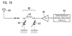
- Fig. 10 is a diagram showing an example of an impedance matching circuit 40 of the radio transmission circuit
- Fig. 11 is a diagram showing timing for switching polarity of the control voltage VC.
- the signal from a transmission signal process circuit 44 is amplified by a high frequency power amplifier 45 at the end of circuit.
- the impedance matching circuit 40 performs impedance matching with an antenna 46.
- the impedance matching circuit 40 is a ⁇ type circuit made up of variable capacitances 41 and 42 and an inductance 43.
- power amplifier circuits have impedance values different largely in accordance with a frequency band to be used and an amplification output power, so this impedance matching circuit 40 is necessary.
- variable capacitance device 11, 11B, 11C or 11D is used as each of the variable capacitances 41 and 42, and it is controlled by the control voltage VC described above.
- the control voltage VC is adjusted so that the capacitance CP of the variable capacitances 41 and 42 is adjusted for realizing impedance matching with the antenna 46.
- variable capacitances 41 and 42 mean “variable capacitance elements (variable capacitors)” as devices realized by the variable capacitance device 11, 11B, 11C or 11D in some cases, and they mean functions realized by the variable capacitance device 11, 11B, 11C or 11D in other cases.
- the control voltage VC is a voltage having a waveform shown in Fig. 3A or 3B , and its polarity changes at a predetermined period T/2 for suppressing generation of space charge KD in the variable capacitances 41 and 42.
- the voltage VS will be lowered at the moment of switching polarity.
- a value of the capacitance CP of the variable capacitances 41 and 42 varies so that the impedance matching may fail.
- polarity of the control voltage VC is changed while the high frequency power amplifier 45 is not working, i.e., not performing transmission.
- the polarity is changed when a signal does not flow in the variable capacitances 41 and 42.
- polarity of the control voltage VC is switched during the time period while the transmission circuit is not performing the transmission.
- the control voltage (1) is an example of the case where it has only the positive voltage VS and the negative voltage VS, and the polarity is changed during an idle period of the transmission circuit.
- the control voltage (2) is an example of the case where it has 0 volt period between the positive voltage VS and the negative voltage VS, and the 0 volt period is set as long as possible in the idle period of the transmission circuit. In this case, it has waveform similar to the control voltage VC2 shown in Fig. 3B , and it is possible to prevent the charge up of the dielectric film 26 more effectively by passing through the 0 volt period.
- control voltage VC for controlling the variable capacitances 41 and 42 is not applied to the high frequency power amplifier 45 and the like.
- various countermeasures such as using capacitor of an appropriate capacitance for cutting low frequency components and an appropriate LC filter for cutting high frequency components.
- variable capacitance device 11, 11B, 11C or 11D is incorporated in a mobile terminal
- timing of changing polarity of the control voltage VC will be described.
- An example of the mobile terminal that is a mobile phone of TDD method (transmission and reception time-division duplex method) will be described.
- GSM Global System for Mobile Communications
- WiMAX Worldwide Interoperability for Microwave Access of IEEE 802.16 standard
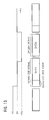
- Fig. 12 is a diagram showing a relationship between transmission/reception sequence of WiMAX and timing for switching polarity of the control voltage VC.
- the transmission and reception is divided by a unit of 5 milliseconds, and one reception and one transmission are performed in turn in each of divided transmission and reception sections KK. More specifically, the mobile terminal receives a reception signal (down link signal) from a base station at the start of each transmission and reception section KK, and then it sends out a transmission signal (up link signal) to the base station.
- a reception signal down link signal
- up link signal up link signal
- the transmission circuit shown in Fig. 10 is in an idle state, during which polarity of the control voltage VC for controlling the variable capacitances 41 and 42 is switched.
- the switching of polarity of the control voltage VC may be performed every time when the transmission circuit becomes the idle state or every plurality of times.
- one change of polarity is performed in six idle states of the transmission circuit, i.e., every time when six transmission and reception sections KK are performed. Therefore, in this case, polarity is changed at a period of 30 milliseconds.
- variable capacitances 41 and 42 made up of the variable capacitance device can be adjusted accurately.
- the polarity of the control voltage VC is switched during the idle period of the transmission circuit, it is possible to avoid the influence of instant variation of the variable capacitances 41 and 42.
- Fig. 13 is a diagram showing another example of a relationship between transmission/reception sequence of WiMAX and timing for switching polarity of the control voltage VC.
- Fig. 12 the polarity of the control voltage VC is switched directly in a reception section of the mobile terminal.
- Fig. 13 the polarity of the control voltage VC is switched after the period of 0 volt.
- the control voltage VC is set to 0 volt at the initial timing, and the polarity of the control voltage VC is changed and raised at the end timing. Therefore, the control voltage VC becomes positive voltage (+VS) or negative voltage (-VS) only during the period that covers the transmission section of the mobile terminal and substantially equal to the same. In this way, the charge up of the dielectric film 26 can be prevented securely so that the variable capacitance device can be controlled accurately by elongating the time while the voltage VS is not applied,
- the time division of the transmission and reception is 5 milliseconds with the radio communication of the WiMAX method, as shown in Fig. 13 .
- the polarity exchange period is 5 milliseconds, the charge up of the dielectric film 26 of the variable capacitance device can be suppressed. There is no problem substantially in the control accuracy of the variable capacitance.
- variable capacitance device when the period of switching polarity of the control voltage VC is 5 milliseconds, if the variation of the capacitance CP from the initial value is 10% or smaller, the variable capacitance device can be applied to the transmission and reception circuit of the mobile terminal of WiMAX.
- material, thickness and the like of the dielectric layer should be selected for making the variable capacitance device that can be applied as described above.
- variable capacitance device 11, 11B, 11C or 11D is incorporated in the mobile terminal as a variable capacitance switch.
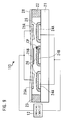
- Fig. 14 is a diagram showing a switching circuit for transmission and reception of the mobile terminal
- Figs. 15A and 15B are diagrams showing an operational state of the variable capacitance switch
- Fig. 16 is a diagram showing a relationship between the switching timing of the transmission/reception and timing for switching polarity of the control voltage VC.
- variable capacitance switches 54 and 55 are provided for connecting an antenna 53 selectively to a reception circuit 51 or a transmission circuit 52 in a switching circuit 50 of transmission and reception.
- the variable capacitance switch 54 is a switch for connecting or disconnecting the antenna 53 and the reception circuit 51
- the variable capacitance switch 55 is a switch for connecting or disconnecting the antenna 53 and the transmission circuit 52. Note that the impedance matching circuit and the like are omitted in the drawing.
- variable capacitance device 11, 11B, 11C or 11D described above is used as the variable capacitance switches 54 and 55, and the control voltage VC is set to a value that is sufficiently large.
- the capacitance CP is changed largely, so that electric impedance is changed largely. Since the radio frequency used in the mobile terminal is in gigahertz band or close to the same, operation realized by changing the capacitance CP is equivalent to the electric switch.
- variable capacitance switch 54 for the reception circuit is turned off, while the variable capacitance switch 55 for the transmission circuit is turned on. Therefore, the antenna 53 is connected to the transmission circuit 52.
- the control voltage VC is not applied to the variable capacitance switch 54.
- the upper electrode 25 is separated from the dielectric film 26, and the capacitance CP is small.
- the maximum voltage VS as the control voltage VC is applied to the variable capacitance switch 55, and the upper electrode 25 is contacting the dielectric film 26 in this state. Therefore, the capacitance CP is very large.
- the variable capacitance switch 54 is turned on while the variable capacitance switch 55 is turned off.
- control voltage VC of the variable capacitance switch 54 for the reception circuit becomes the predetermined voltage VS in the reception, while it becomes 0 volt in the transmission.
- the polarity of the control voltage VC is switched every time when it becomes the reception section.
- control voltage VC of the variable capacitance switch 55 for the transmission circuit becomes the predetermined voltage VS in the transmission, while it becomes 0 volt in the reception.
- the polarity of the control voltage VC is switched every time when it becomes the transmission section.
- variable capacitance device 11, 11B, 11C or 11D is used as the variable capacitance switches 54 and 55 by switching the polarity of the control voltage VC at an appropriate period.
- variable capacitance element a variable capacitance switch, an impedance matching circuit or a transmission and reception switching circuit that enables more accurate control than the conventional one by suppressing occurrence of hysteresis.
- the structure, the shape, the material, the numbers and the like of the variable capacitance device 11, 11B, 11C can be modified variously. Furthermore, the structure, the shape, the size, the number, the material of a whole or a part of the variable capacitance device, the impedance matching circuit 40, the variable capacitance switches 54 and 55, the driving circuit 12 and the micro machine system 3, the circuit structure, the waveform of the control voltage VC, the switching timing of the polarity, the period or the frequency, and the like can be modified if necessary in accordance with the spirit of the present invention.
- variable capacitance device as the micro machine device
- the same effect can be expected by changing the polarity of the control voltage VC at regular intervals also with respect to other micro machine device in which charge up may occur by the control voltage VC.
Landscapes
- Engineering & Computer Science (AREA)
- Power Engineering (AREA)
- Microelectronics & Electronic Packaging (AREA)
- Computer Hardware Design (AREA)
- Micromachines (AREA)
Applications Claiming Priority (1)
| Application Number | Priority Date | Filing Date | Title |
|---|---|---|---|
| JP2007013281A JP4919819B2 (ja) | 2007-01-24 | 2007-01-24 | マイクロマシンデバイスの駆動制御方法および装置 |
Publications (2)
| Publication Number | Publication Date |
|---|---|
| EP1950778A2 true EP1950778A2 (fr) | 2008-07-30 |
| EP1950778A3 EP1950778A3 (fr) | 2009-03-11 |
Family
ID=39432537
Family Applications (1)
| Application Number | Title | Priority Date | Filing Date |
|---|---|---|---|
| EP08100445A Withdrawn EP1950778A3 (fr) | 2007-01-24 | 2008-01-14 | Procédé de contrôle de commande et unité pour dispositif de micro-machine |
Country Status (5)
| Country | Link |
|---|---|
| US (1) | US7961448B2 (fr) |
| EP (1) | EP1950778A3 (fr) |
| JP (1) | JP4919819B2 (fr) |
| KR (1) | KR20080069898A (fr) |
| CN (2) | CN102800478B (fr) |
Cited By (1)
| Publication number | Priority date | Publication date | Assignee | Title |
|---|---|---|---|---|
| US9224536B2 (en) | 2010-02-08 | 2015-12-29 | Murata Manufacturing Co., Ltd. | Variable capacitance device |
Families Citing this family (13)
| Publication number | Priority date | Publication date | Assignee | Title |
|---|---|---|---|---|
| JP4610576B2 (ja) * | 2007-03-30 | 2011-01-12 | 富士通株式会社 | マイクロマシンデバイスの駆動制御方法および装置 |
| JP5363005B2 (ja) | 2008-02-20 | 2013-12-11 | 富士通株式会社 | 可変容量素子、整合回路素子、および携帯端末装置 |
| JP4737253B2 (ja) * | 2008-08-29 | 2011-07-27 | ソニー株式会社 | 非接触受信装置 |
| JP5304398B2 (ja) * | 2009-04-06 | 2013-10-02 | 富士通株式会社 | 可変容量素子 |
| JP5338615B2 (ja) * | 2009-10-27 | 2013-11-13 | 富士通株式会社 | 可変容量デバイスおよび可変容量素子の駆動方法 |
| TW201140637A (en) * | 2009-11-26 | 2011-11-16 | Taiyo Yuden Kk | Mems switch |
| JP5418317B2 (ja) * | 2010-03-11 | 2014-02-19 | 富士通株式会社 | 静電アクチュエータ、およびその駆動方法 |
| CN102243941B (zh) * | 2011-04-08 | 2013-07-31 | 东南大学 | 具有低驱动电压的射频微机械系统电容式并联开关 |
| US9219478B2 (en) * | 2013-05-15 | 2015-12-22 | Hui-Hu Liang | Circuit switch for keyboard |
| JP6225526B2 (ja) * | 2013-07-17 | 2017-11-08 | 株式会社デンソー | 加振装置 |
| US9590686B2 (en) * | 2013-12-26 | 2017-03-07 | Google Technology Holdings LLC | Maintaining a capacitor dielectric under strain to reduce capacitance variation due to time variant hysterisis effect |
| JP6595422B2 (ja) * | 2016-08-24 | 2019-10-23 | 株式会社東芝 | センサ及び電子機器 |
| CN114976607B (zh) * | 2021-02-24 | 2024-03-12 | 北京京东方技术开发有限公司 | 天线和通信设备 |
Citations (3)
| Publication number | Priority date | Publication date | Assignee | Title |
|---|---|---|---|---|
| JP2002036197A (ja) | 2000-04-13 | 2002-02-05 | Nokia Mobile Phones Ltd | マイクロマシン素子を制御するための方法および装置 |
| JP2002084148A (ja) | 2000-06-27 | 2002-03-22 | Nokia Mobile Phones Ltd | 増幅器を負荷インピーダンスに適応させるための整合回路と方法 |
| US6391675B1 (en) | 1998-11-25 | 2002-05-21 | Raytheon Company | Method and apparatus for switching high frequency signals |
Family Cites Families (20)
| Publication number | Priority date | Publication date | Assignee | Title |
|---|---|---|---|---|
| DE4041271C2 (de) * | 1989-12-25 | 1998-10-08 | Toshiba Kawasaki Kk | Halbleitervorrichtung mit einem ferroelektrischen Kondensator |
| JPH03284817A (ja) | 1989-12-25 | 1991-12-16 | Toshiba Corp | 強誘電体コンデンサ |
| US5619061A (en) * | 1993-07-27 | 1997-04-08 | Texas Instruments Incorporated | Micromechanical microwave switching |
| JPH08107245A (ja) | 1994-10-05 | 1996-04-23 | Meidensha Corp | パルス電源 |
| JP3284817B2 (ja) | 1995-03-27 | 2002-05-20 | 日産自動車株式会社 | エンジンの失火診断装置 |
| JPH10154456A (ja) * | 1996-11-25 | 1998-06-09 | Omron Corp | マイクロリレー、その製造方法およびその制御方法 |
| JPH11111566A (ja) * | 1997-10-07 | 1999-04-23 | Sharp Corp | インピーダンス整合器 |
| JP3437520B2 (ja) * | 2000-03-01 | 2003-08-18 | キヤノン株式会社 | 静電アクチュエータ駆動機構、静電アクチュエータ駆動方法、及びこれらによる静電アクチュエータ、回転ステージ、ポリゴンミラー |
| US6806988B2 (en) * | 2000-03-03 | 2004-10-19 | Canon Kabushiki Kaisha | Optical apparatus |
| US6509745B1 (en) * | 2000-09-25 | 2003-01-21 | Detroit Diesel Corporation | Method and apparatus for measuring liquid dielectric behavior |
| JP4151338B2 (ja) * | 2002-07-30 | 2008-09-17 | 松下電器産業株式会社 | 可変容量素子とその形成方法 |
| US7106066B2 (en) * | 2002-08-28 | 2006-09-12 | Teravicta Technologies, Inc. | Micro-electromechanical switch performance enhancement |
| JP2004140597A (ja) * | 2002-10-17 | 2004-05-13 | Hitachi Metals Ltd | アンテナ送受信切替え回路 |
| EP1662308A4 (fr) * | 2003-08-21 | 2011-03-02 | Olympus Corp | Actionneur electrostatique, dispositif obturateur, module d'imagerie, et camera |
| US7142072B2 (en) * | 2003-09-22 | 2006-11-28 | Kyocera Corporation | Variable matching circuit, variable resonance circuit, variable phase-shifting circuit and variable attenuation circuit each having variable-capacitance capacitor |
| JP4325930B2 (ja) | 2003-12-17 | 2009-09-02 | 京セラ株式会社 | 可変移相回路 |
| KR100565800B1 (ko) * | 2003-12-22 | 2006-03-29 | 삼성전자주식회사 | 단일 전극을 이용한 mems 구조물의 구동 및 구동검지장치 |
| KR100599115B1 (ko) * | 2004-07-20 | 2006-07-12 | 삼성전자주식회사 | 진동형 멤스 스위치 및 그 제조방법 |
| US20060125746A1 (en) * | 2004-12-13 | 2006-06-15 | Jean-Michel Sallese | Microelectrical device |
| JP4643316B2 (ja) * | 2005-03-11 | 2011-03-02 | 株式会社東芝 | マイクロマシンスイッチ及びその駆動方法 |
-
2007
- 2007-01-24 JP JP2007013281A patent/JP4919819B2/ja not_active Expired - Fee Related
- 2007-10-26 KR KR1020070108399A patent/KR20080069898A/ko not_active Ceased
-
2008
- 2008-01-14 EP EP08100445A patent/EP1950778A3/fr not_active Withdrawn
- 2008-01-23 US US12/010,243 patent/US7961448B2/en not_active Expired - Fee Related
- 2008-01-24 CN CN201210247006.XA patent/CN102800478B/zh not_active Expired - Fee Related
- 2008-01-24 CN CN2008100087067A patent/CN101231921B/zh not_active Expired - Fee Related
Patent Citations (3)
| Publication number | Priority date | Publication date | Assignee | Title |
|---|---|---|---|---|
| US6391675B1 (en) | 1998-11-25 | 2002-05-21 | Raytheon Company | Method and apparatus for switching high frequency signals |
| JP2002036197A (ja) | 2000-04-13 | 2002-02-05 | Nokia Mobile Phones Ltd | マイクロマシン素子を制御するための方法および装置 |
| JP2002084148A (ja) | 2000-06-27 | 2002-03-22 | Nokia Mobile Phones Ltd | 増幅器を負荷インピーダンスに適応させるための整合回路と方法 |
Cited By (1)
| Publication number | Priority date | Publication date | Assignee | Title |
|---|---|---|---|---|
| US9224536B2 (en) | 2010-02-08 | 2015-12-29 | Murata Manufacturing Co., Ltd. | Variable capacitance device |
Also Published As
| Publication number | Publication date |
|---|---|
| CN102800478A (zh) | 2012-11-28 |
| EP1950778A3 (fr) | 2009-03-11 |
| CN101231921B (zh) | 2012-08-22 |
| CN101231921A (zh) | 2008-07-30 |
| KR20080069898A (ko) | 2008-07-29 |
| US20080180872A1 (en) | 2008-07-31 |
| JP4919819B2 (ja) | 2012-04-18 |
| JP2008181725A (ja) | 2008-08-07 |
| CN102800478B (zh) | 2016-02-10 |
| US7961448B2 (en) | 2011-06-14 |
Similar Documents
| Publication | Publication Date | Title |
|---|---|---|
| EP1950778A2 (fr) | Procédé de contrôle de commande et unité pour dispositif de micro-machine | |
| JP4188805B2 (ja) | Mems可変インダクタ及びキャパシタ | |
| JP3890952B2 (ja) | 容量可変型キャパシタ装置 | |
| JP4555951B2 (ja) | MEMS(Micro−Electro−Mechanical−System)素子のアレイの駆動 | |
| KR101041326B1 (ko) | 가변 용량 소자, 정합 회로 소자, 및 휴대 단말 장치 | |
| EP1346382A2 (fr) | Condensateur variable etage a commutation mems et son procede de fabrication | |
| EP1385189A2 (fr) | Commutateur | |
| CN101438366A (zh) | 微机电系统(mems)可变电容器、激励部件及相关方法 | |
| KR20090057973A (ko) | 전자 소자, 가변 커패시터, 마이크로스위치, 마이크로스위치의 구동 방법, 및 mems형 전자 소자 | |
| US8363381B2 (en) | Variable capacitive element, variable capacitive device, and method for driving the variable capacitive element | |
| JP5176148B2 (ja) | スイッチング素子および通信機器 | |
| JP5821967B2 (ja) | 可動電極を有する電気機器 | |
| US9087929B2 (en) | Variable capacitance device | |
| EP1843368A1 (fr) | Circuit de commutation | |
| JP4842041B2 (ja) | スイッチ | |
| JP5130291B2 (ja) | 電気機械素子およびそれを用いた電気機器 | |
| KR100357164B1 (ko) | 마이크로 가변 커패시터 | |
| Busquere et al. | Above IC MEMS capacitors for integrated reconfigurable circuits | |
| KR20060070957A (ko) | 정전기력 구동 rf mems 스위치 및 그 제조 방법 | |
| WO2003083886A1 (fr) | Dispositif de commutation | |
| KR20040103039A (ko) | 잔류응력 및 압전구동력을 이용한 초소형 전기 기계시스템 고주파 스위치 |
Legal Events
| Date | Code | Title | Description |
|---|---|---|---|
| PUAI | Public reference made under article 153(3) epc to a published international application that has entered the european phase |
Free format text: ORIGINAL CODE: 0009012 |
|
| AK | Designated contracting states |
Kind code of ref document: A2 Designated state(s): AT BE BG CH CY CZ DE DK EE ES FI FR GB GR HR HU IE IS IT LI LT LU LV MC MT NL NO PL PT RO SE SI SK TR |
|
| AX | Request for extension of the european patent |
Extension state: AL BA MK RS |
|
| PUAL | Search report despatched |
Free format text: ORIGINAL CODE: 0009013 |
|
| AK | Designated contracting states |
Kind code of ref document: A3 Designated state(s): AT BE BG CH CY CZ DE DK EE ES FI FR GB GR HR HU IE IS IT LI LT LU LV MC MT NL NO PL PT RO SE SI SK TR |
|
| AX | Request for extension of the european patent |
Extension state: AL BA MK RS |
|
| RIC1 | Information provided on ipc code assigned before grant |
Ipc: H03H 7/38 20060101ALI20090204BHEP Ipc: B81B 3/00 20060101ALI20090204BHEP Ipc: H01P 1/12 20060101ALI20090204BHEP Ipc: H01H 1/00 20060101ALI20090204BHEP Ipc: H01G 5/18 20060101AFI20080613BHEP |
|
| AKX | Designation fees paid | ||
| STAA | Information on the status of an ep patent application or granted ep patent |
Free format text: STATUS: THE APPLICATION IS DEEMED TO BE WITHDRAWN |
|
| 18D | Application deemed to be withdrawn |
Effective date: 20090912 |
|
| REG | Reference to a national code |
Ref country code: DE Ref legal event code: 8566 |