EP1950875A1 - Einschaltstrom-verringerungsschaltung und elektrische einrichtung - Google Patents
Einschaltstrom-verringerungsschaltung und elektrische einrichtung Download PDFInfo
- Publication number
- EP1950875A1 EP1950875A1 EP06812036A EP06812036A EP1950875A1 EP 1950875 A1 EP1950875 A1 EP 1950875A1 EP 06812036 A EP06812036 A EP 06812036A EP 06812036 A EP06812036 A EP 06812036A EP 1950875 A1 EP1950875 A1 EP 1950875A1
- Authority
- EP
- European Patent Office
- Prior art keywords
- circuit
- rush current
- transistor
- diode bridge
- voltage
- Prior art date
- Legal status (The legal status is an assumption and is not a legal conclusion. Google has not performed a legal analysis and makes no representation as to the accuracy of the status listed.)
- Withdrawn
Links
Images


Classifications
-
- H—ELECTRICITY
- H02—GENERATION; CONVERSION OR DISTRIBUTION OF ELECTRIC POWER
- H02M—APPARATUS FOR CONVERSION BETWEEN AC AND AC, BETWEEN AC AND DC, OR BETWEEN DC AND DC, AND FOR USE WITH MAINS OR SIMILAR POWER SUPPLY SYSTEMS; CONVERSION OF DC OR AC INPUT POWER INTO SURGE OUTPUT POWER; CONTROL OR REGULATION THEREOF
- H02M7/00—Conversion of AC power input into DC power output; Conversion of DC power input into AC power output
- H02M7/02—Conversion of AC power input into DC power output without possibility of reversal
- H02M7/04—Conversion of AC power input into DC power output without possibility of reversal by static converters
- H02M7/12—Conversion of AC power input into DC power output without possibility of reversal by static converters using discharge tubes with control electrode or semiconductor devices with control electrode
- H02M7/125—Avoiding or suppressing excessive transient voltages or currents
-
- H—ELECTRICITY
- H02—GENERATION; CONVERSION OR DISTRIBUTION OF ELECTRIC POWER
- H02M—APPARATUS FOR CONVERSION BETWEEN AC AND AC, BETWEEN AC AND DC, OR BETWEEN DC AND DC, AND FOR USE WITH MAINS OR SIMILAR POWER SUPPLY SYSTEMS; CONVERSION OF DC OR AC INPUT POWER INTO SURGE OUTPUT POWER; CONTROL OR REGULATION THEREOF
- H02M7/00—Conversion of AC power input into DC power output; Conversion of DC power input into AC power output
- H02M7/42—Conversion of DC power input into AC power output without possibility of reversal
- H02M7/44—Conversion of DC power input into AC power output without possibility of reversal by static converters
- H02M7/48—Conversion of DC power input into AC power output without possibility of reversal by static converters using discharge tubes with control electrode or semiconductor devices with control electrode
- H02M7/53—Conversion of DC power input into AC power output without possibility of reversal by static converters using discharge tubes with control electrode or semiconductor devices with control electrode using devices of a triode or transistor type requiring continuous application of a control signal
- H02M7/537—Conversion of DC power input into AC power output without possibility of reversal by static converters using discharge tubes with control electrode or semiconductor devices with control electrode using devices of a triode or transistor type requiring continuous application of a control signal using semiconductor devices only, e.g. single switched pulse inverters
-
- H—ELECTRICITY
- H02—GENERATION; CONVERSION OR DISTRIBUTION OF ELECTRIC POWER
- H02M—APPARATUS FOR CONVERSION BETWEEN AC AND AC, BETWEEN AC AND DC, OR BETWEEN DC AND DC, AND FOR USE WITH MAINS OR SIMILAR POWER SUPPLY SYSTEMS; CONVERSION OF DC OR AC INPUT POWER INTO SURGE OUTPUT POWER; CONTROL OR REGULATION THEREOF
- H02M1/00—Details of apparatus for conversion
- H02M1/12—Arrangements for reducing harmonics from AC input or output
Definitions
- the present invention relates to a rush current reduction circuit in which the number of circuit elements can be decreased, and an electric appliance.
- an inverter instrument realizes improved efficiency and reduction in size and weight of a power supply transformer by shifting the switching frequency to a high frequency.
- power supply filters are installed for preventing electromagnetic interference to the other appliances.
- these power supply filters are designed considering only the condition that the instrument is continuously operating. It is usual that power is applied to instruments when only it is necessary to operate while the power supply is cut off to stop the operation when it is unnecessary to operate, with considering efficiency of power supply utilization or energy saving, and accordingly turning on/off of the power supply occurs more frequently than in the past.
- the Japanese Laid-Open Patent Publication No. H05-19879 discloses a technique for making current (drain current) flowing through a power supply line constant, by adjusting its gate voltage with a voltage divider while inserting a MOSFET in the power supply line.
- transient electromagnetic disturbance increases accompanied by power supply on/off, with a power supply filter circuit involved.
- Generation of the transient current when the power supply is turned on or cut off for the electric appliances is conventionally known; however the number of reports with respect to magnitude of the rush current of inverter instruments are very small.
- the rush current affects the whole of the power distribution system, and the quality of the power supply; and accordingly if the rush current is not suppressed, it becomes difficult to stably supply power.
- an AC rush current reduction circuit provided with both a circuit for reducing the rush current in positive direction and a circuit for reducing the rush current in negative direction.
- the present invention is achieved in consideration of the above described problem and its object is to provide a rush current reduction circuit and electric appliance capable of reducing the number of circuit elements.
- a first aspect of the present invention provides a rush current reduction circuit provided with a diode bridge inserted in an AC circuit into which a load circuit is inserted, and a DC rush current reduction circuit inserted into a circuit through which current flows from the diode bridge.
- a second aspect of the present invention provides a rush current reduction circuit provided with a diode bridge inserted into an AC circuit when a load circuit is connected to subsequent stages of the diode bridge inserted into the AC circuit, and a DC rush current reduction circuit inserted into a circuit through which current flows from the diode bridge.
- a third aspect of the present invention which is the rush current reduction circuit according to the second aspect, provides a control circuit from a first circuit node existing in the subsequent stages of the diode bridge to which a load circuit is connected, to a second circuit node existing in a DC rush current reduction circuit.
- a fourth aspect of the present invention is the rush current reduction circuit according to the third aspect, here, in which the control circuit is provided with a diode for preventing reverse current to the first circuit node.
- a fifth aspect of the present invention provides an electric appliance provided with the rush current reduction circuit and the load circuit in any one of the first to the fourth aspects.
- a sixth aspect of the present invention which is an electric appliance according to the fifth aspect, is provided with a drive unit in which power is supplied from an inverter to be the load circuit.
- a seventh aspect of the present invention which is the electric appliance according to the fifth aspect, is provided with a light source in which power is supplied from the inverter to be the load circuit.
- the present invention it is possible to reduce the number of the circuit elements, by inserting the DC rush current reduction circuit into the circuit through which current flows from the diode bridge, compared with a case where the AC rush current reduction circuit is inserted into the AC circuit.
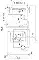
- Fig. 1 is a circuit diagram of an electric appliance using a rush current reduction circuit according to a first embodiment.
- This electric appliance is used together with a single phase AC power supply 1, and is provided with an inverter 2 to which power is supplied by this AC power supply 1, that is, which becomes a load circuit for the AC power supply 1.
- the electric appliance is further provided with, for instance, a light source 3 to which power is supplied by the inverter 2.
- One pole of the AC power supply 1 is connected to one AC input node of a diode bridge DB1 via one switch SW1 of a double-pole switch and one inductance L constituting a noise filter NF.
- the other AC input node of the diode bridge DB1 is connected to one AC input node of a diode bridge DB2 via the other inductance L constituting the noise filter NF.
- the other AC input node of the diode bridge DB2 is connected to the other pole of the AC power supply 1 via the other switch SW2 of the double-pole switch.
- capacitors C are connected between the input nodes and between output nodes.
- An output node (pulsating current output node) at a plus side of the diode bridge DB2 is connected to a drain of a transistor Q1 to be an N-channel MOSFET (field effect transistor); and a source of the transistor Q1 is connected to an output node at a minus side of the diode bridge DB2.
- the output contact point of the diode bridge DB2 is connected between the source/drain of the transistor Q1 in parallel.
- One end of a resister R1 is connected to the drain of the transistor Q1, and the other end of the resister R1 is connected to a gate of the transistor Q1.
- One end of a resister R2 is connected to the gate of the transistor Q1, and the other end of the resister R2 is connected to the source of the transistor Q1.
- the capacitor C1 is connected to the resister R2 in parallel.
- a circuit comprised of these transistor Q1, resisters R1, R2 and capacitor C1 constitutes a DC rush current reduction circuit 5 in the present embodiment. That is, the DC rush current reduction circuit 5 is constituted from the transistor Q1 of which the drain is connected to the output contact point at the plus side of the diode bridge DB2, the resister R1 connected between the drain/gate of the transistor Q1, the resister R2 connected between the source/drain of the transistor Q1, and the capacitor C1 connected in parallel to the resister R2. In addition, the DC rush current reduction circuit 5 is connected between the AC power supply 1 and the noise filter NF. Meanwhile, AC voltage output from the AC power supply 1 is applied between AC input contact points of the diode bridge DB2 via the noise filter NF.
- the output node at the plus side of the diode bridge DB1 is connected to the input node at the plus side of an inverter 2, and the output node at the minus side of the diode bridge DB1 is connected to the input node at the minus side of the inverter 2.
- an electrolytic capacitor 2A having relatively large capacitance is connected between the input nodes, and the respective input nodes are connected to respective input nodes of a voltage conversion circuit 2B.
- One end of a resister R3 is connected to the output node at a plus side of the voltage conversion circuit 2B, and the other end of the resister R3 is connected to the gate of the transistor Q1.
- a circuit from the output node at the plus side of the voltage conversion circuit 2B to the gate of the transistor Q1 constitutes a control circuit 6 of the present embodiment.
- the output node at the minus side of the voltage conversion circuit 2B is connected to the input node at the minus side of the voltage conversion circuit 2B, and further, the light source 3 is connected between the output node at the minus side and the output node at the plus side of the conversion circuit 2B.
- the voltage conversion circuit 2B steps up or down the voltage, and causes the light source 3 to emit light by applying the voltage.
- the resistance values of the resister R1 and the resister R2 may be set such that the gate voltage becomes sufficiently high, and further, the electric capacitance of the capacitor C1 and the resistance values of the resistor R1 and the resister R2 may be set such that the capacitor C1 is not discharged.
- Fig. 2 is an equivalent circuit diagram of a case where voltage of a pole at the switch SW1 side of the AC power supply 1 is higher; and Fig. 3 is an equivalent circuit diagram of a case where voltage of a pole at the switch SW2 side of the AC power supply 1 is higher.
- the AC power supply 1 is shown with a symbol of a DC power supply.
- the double-pole switch is omitted as the switches SW1 and SW2 of the double-pole switch are turned ON.
- the noise filter NF is omitted.
- diode bridges DB1 and DB2 there are indicated only diodes electrically conducted.
- a diode D11 connected between the output node at its plus side and an AC input node at the diode bridge DB2 side is electrically conducted.
- a diode D12 connected between an output node at its minus side and an AC input node of the other is electrically conducted.
- a diode D21 connected between an output node at its plus side and an AC input node at the diode bridge DB2 side is electrically conducted.
- a diode D22 connected between an output node at its minus side and an AC input node of the other is electrically conducted.
- the potential of the output node at the plus side of the voltage conversion circuit 2B is higher than that of the gate of the transistor Q1. Therefore, the charge of the capacitor C1 is not discharged toward the output node at the plus side of the voltage conversion circuit 2B.
- a diode D13 connected between an output node at its plus side and an AC input node at the diode bridge DB2 side is electrically conducted.
- a diode D14 connected between an output node at its minus side and an AC input node of the other is electrically conducted.
- a diode D23 connected between the output node at its plus side and the AC input node at the diode bridge DB1 side is electrically conducted.
- a diode D24 connected between the output node at its minus side and the AC input node of the other is electrically conducted.
- the potential of the output node of the plus side of the voltage conversion circuit 2B is lower than that of the gate of the transistor Q1.
- the light source 3 includes elements which emit light at a lower voltage like an LED (light-emitting diode)
- the potential of the output node at the plus side of the voltage conversion circuit 2B becomes lower than the potential of the gate of the transistor Q1.
- the charge of the capacitor C1 is discharged toward the output node at the plus side of the voltage conversion circuit 2B; it is not possible to keep the gate voltage of the transistor Q1 high. For that reason, the electric appliance exerts effects, when, for instance, the light source 3 includes elements which emit light with high voltage like a fluorescent tube and the potential difference between the output nodes of the voltage conversion circuit 2B is large.
- the DC rush current reduction circuit 5 by inserting the DC rush current reduction circuit 5 into the circuit through which current flows from the diode bridge DB2, it is possible to reduce (approximately be reduced by half) the number of the circuit elements, compared with the case where the AC rush current reduction circuit constituted in such a way as to oppositely connect the aforementioned DC rush current reduction circuit 5 is inserted into the circuit from one pole to the other pole of the AC circuit, that is, the AC power supply 1.
- the diode bridge DB2 is inserted into the AC circuit when the inverter 2 (load circuit) is connected to subsequent stages of the diode bridge DB1 inserted into the AC circuit, and the DC rush current reduction circuit 5 is inserted into the circuit through which current flows from the diode bridge DB2, for instance, the DC rush current reduction circuit 5 may be inserted into the circuit through which current flows from the diode bridge DB2; while inserting the diode bridge DB2 into the AC circuit into which the load circuit such as AC motor is inserted, is also effective.
- the control circuit 6 the circuit from the output node at the plus side of the voltage conversion circuit 2B to the gate of the transistor Q1 from a first circuit node existing in subsequent stages of the diode bridge DB1 to a second circuit node existing in the DC rush current reduction circuit 5, the first embodiment is preferable for the cases where the potential difference between the output nodes of the voltage conversion circuit 2B is large.
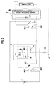
- Fig. 4 is a circuit diagram of the electric appliance using the rush current reduction circuit 5 according to the second embodiment.
- the potential of the output node at the plus side of the voltage conversion circuit 2B becomes higher than that of the gate of the transistor Q1. Therefore, the charge of the capacitor C1 is not discharged toward the output node at the plus side of the voltage conversion circuit 2B.
- Fig. 5 is an equivalent circuit diagram of a case where voltage of a pole at the switch SW2 side of the AC power supply 1 is higher.
- the AC power supply 1 is shown with a symbol of a DC power supply.
- the switches SW1 and SW2 of the double-pole switch are omitted as the switches SW1 and SW2 of the double-pole switch are turned ON.
- the noise filter NF is omitted.
- the diode bridges DB1 and DB2 there are indicated only diodes electrically conducted.
- the potential of the output node at the plus side of the voltage conversion circuit 2B is lower than that of the gate of the transistor Q1.
- the electric appliance according to the second embodiment is used in cases where the light source 3 includes elements which emit light with high voltage like a fluorescent tube and the potential difference between the output nodes of the voltage conversion circuit 2B is large, and further, the electric appliance according to the second embodiment is also used in cases where the light source 3 includes elements which emit light with low voltage like an LED and the potential difference between the output nodes of the voltage conversion circuit 2B is small.
- the control circuit 6 (circuit from the output node at the plus side of the voltage conversion circuit 2B to the gate of the transistor Q1) is preferable even the case where the potential difference between the output nodes of the voltage conversion circuit 2B is small, because there is provided the diode D1 for preventing reverse current toward the first circuit node (output node at the plus side of the voltage conversion circuit 2B).
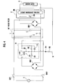
- the circuit of the comparative example has the AC power supply 1, the switches SW1 and SW2 constituting double-pole switch provided respectively to both poles of the AC power supply, the noise filter NF connected in parallel to the switches SW1 and SW2, the diode bridge DB1 whose input node is connected in parallel to the output node of the noise filter NF, and the inverter 2 connected in parallel to the output contact point of the diode bridge DB1.
- the inverter 2 has the voltage conversion circuit 2B and the electrolytic capacitor 2A connected in parallel to the input node of the voltage conversion circuit 2B.
- the circuit of the comparative example differs in that the circuit of the comparative example is not provided with the diode bridge DB2, the rush current reduction circuit 5, and the control circuit 6; and with respect to the other points, both circuits are in common.
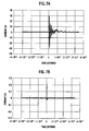
- Fig. 7A shows variation of the current measured with a current measurement device inserted between the AC power supply 1 and the switch SW1 of the circuit of the comparative example described above.
- a horizontal axis denotes time.
- control circuit 6 may not be provided.
- the control circuit 6 is provided between the output node at the plus side of the voltage conversion circuit 2B and the gate of the transistor Q1; however, instead of this, the control circuit 6 may be provided between the node at the plus side of the electrolytic capacitor 2A and the gate of the transistor Q1. This configuration is applied to the case where lighting instruments emit light with alternating current, such as fluorescent tubes, are used as the light source 3.
- a graph shown in Fig. 7B is a result of the case where the control circuit 6 is provided between the node at the plus side of the electrolytic capacitor 2A and the gate of the transistor Q1.
- the electric appliances of these embodiments may be ones which are provided with a drive unit instead of the light source 3.
- the voltage conversion circuit 2B sets up or down the voltage, and then the voltage conversion circuit 2B applies the voltage to the drive unit to drive the drive unit.
- the operations other than this are the same as those of the above. Therefore, it is possible to reduce the number of circuit elements of the electric appliance provided with the drive unit.
- the N channel MOSFET is used; however, also an NPN bipolar transistor may be used. Also, P channel MOSFET or PNP bipolar transistor may be used. In addition, the double-pole switch is used in these embodiments; however, a single-pole switch may be used.
- the rush current reduction circuit it is possible to prevent the electromagnetic interferences generated not only at a continuous operation of general electric appliance in which inverter technique is applied but also at the time of activation. Consequently, in various industrial fields, through reduction of adverse effect for the other electric appliance, there is prevented malfunction, and thus contributing to improvement of safety.
Landscapes
- Engineering & Computer Science (AREA)
- Power Engineering (AREA)
- Inverter Devices (AREA)
- Rectifiers (AREA)
- Emergency Protection Circuit Devices (AREA)
- Control Of Electrical Variables (AREA)
- Circuit Arrangement For Electric Light Sources In General (AREA)
Applications Claiming Priority (2)
| Application Number | Priority Date | Filing Date | Title |
|---|---|---|---|
| JP2005306161A JP3990421B2 (ja) | 2005-10-20 | 2005-10-20 | 突入電流低減回路および電気機器 |
| PCT/JP2006/320858 WO2007046471A1 (ja) | 2005-10-20 | 2006-10-19 | 突入電流低減回路および電気機器 |
Publications (2)
| Publication Number | Publication Date |
|---|---|
| EP1950875A1 true EP1950875A1 (de) | 2008-07-30 |
| EP1950875A4 EP1950875A4 (de) | 2011-10-19 |
Family
ID=37962564
Family Applications (1)
| Application Number | Title | Priority Date | Filing Date |
|---|---|---|---|
| EP06812036A Withdrawn EP1950875A4 (de) | 2005-10-20 | 2006-10-19 | Einschaltstrom-verringerungsschaltung und elektrische einrichtung |
Country Status (6)
| Country | Link |
|---|---|
| US (1) | US8120930B2 (de) |
| EP (1) | EP1950875A4 (de) |
| JP (1) | JP3990421B2 (de) |
| KR (1) | KR100994525B1 (de) |
| CN (1) | CN101292416B (de) |
| WO (1) | WO2007046471A1 (de) |
Families Citing this family (6)
| Publication number | Priority date | Publication date | Assignee | Title |
|---|---|---|---|---|
| US8422179B2 (en) * | 2009-07-22 | 2013-04-16 | Intersil Americas Inc. | Inrush current control |
| JP2012004253A (ja) | 2010-06-15 | 2012-01-05 | Panasonic Corp | 双方向スイッチ、2線式交流スイッチ、スイッチング電源回路および双方向スイッチの駆動方法 |
| JP5213940B2 (ja) * | 2010-11-24 | 2013-06-19 | エヌ・ティ・ティ・アドバンステクノロジ株式会社 | 突入電流低減回路および電気機器 |
| JP2012248093A (ja) * | 2011-05-30 | 2012-12-13 | Panasonic Corp | 2線式の負荷制御装置 |
| TWI455432B (zh) * | 2012-01-20 | 2014-10-01 | Macroblock Inc | 動態阻尼模組及其應用之驅動電路 |
| CN116761303A (zh) | 2023-06-29 | 2023-09-15 | 厦门普为光电科技有限公司 | 具有瞬态电流抑制功能的照明装置 |
Family Cites Families (23)
| Publication number | Priority date | Publication date | Assignee | Title |
|---|---|---|---|---|
| JPS5154226U (de) * | 1974-10-24 | 1976-04-24 | ||
| JPS5154226A (ja) | 1974-11-07 | 1976-05-13 | Fuji Electric Co Ltd | Handotaihenkansochi |
| JPS5829696B2 (ja) * | 1976-11-26 | 1983-06-24 | 株式会社東芝 | 半導体限流装置 |
| JPS5950781A (ja) * | 1982-09-14 | 1984-03-23 | Matsushita Electric Works Ltd | 電源装置 |
| JPS62104529A (ja) | 1985-10-31 | 1987-05-15 | キユーピー株式会社 | 噴霧式水耕栽培装置 |
| US5109185A (en) * | 1989-09-29 | 1992-04-28 | Ball Newton E | Phase-controlled reversible power converter presenting a controllable counter emf to a source of an impressed voltage |
| JPH03126397A (ja) | 1989-10-12 | 1991-05-29 | Matsushita Electric Ind Co Ltd | 所在応答型ワイヤレスリモコン発信器 |
| JPH03126397U (de) * | 1990-04-04 | 1991-12-19 | ||
| KR930006890B1 (ko) | 1991-04-23 | 1993-07-24 | 삼성전자 주식회사 | 단일 펄스에 의한 전원 구동회로 |
| US5404082A (en) | 1993-04-23 | 1995-04-04 | North American Philips Corporation | High frequency inverter with power-line-controlled frequency modulation |
| JPH08140354A (ja) | 1994-11-10 | 1996-05-31 | Tamura Seisakusho Co Ltd | 昇圧型アクティブフィルタの突入電流防止回路 |
| JPH08140260A (ja) * | 1994-11-10 | 1996-05-31 | Nec Corp | 電源装置 |
| US6057652A (en) * | 1995-09-25 | 2000-05-02 | Matsushita Electric Works, Ltd. | Power supply for supplying AC output power |
| KR100310100B1 (ko) * | 1996-07-10 | 2001-12-17 | 윤종용 | 휴대용 컴퓨터시스템의 전원공급장치 그리고 이에 적합한 dc입력선택회로 |
| KR19980084964A (ko) | 1997-05-27 | 1998-12-05 | 이형도 | 전원공급장치의 돌입전류 제한회로 |
| WO1999012240A1 (de) | 1997-09-02 | 1999-03-11 | Siemens Aktiengesellschaft | Schaltungsanordnung und verfahren zur strombegrenzung für wechselstromverbraucher |
| JP4441029B2 (ja) * | 1999-12-21 | 2010-03-31 | 富士通株式会社 | 電源装置、その制御方法および電源システム |
| US6853097B2 (en) * | 2001-10-03 | 2005-02-08 | Mitsubishi Denki Kabushiki Kaisha | Uniterruptible power supply and its starting method |
| JP2004166445A (ja) | 2002-11-15 | 2004-06-10 | Rohm Co Ltd | 直流−交流変換装置、及びそのコントローラic |
| JP2004303466A (ja) * | 2003-03-28 | 2004-10-28 | Canon Inc | ヒータ駆動回路 |
| JP2005073405A (ja) * | 2003-08-25 | 2005-03-17 | Sony Corp | 突入電流抑制回路 |
| JP2005074305A (ja) | 2003-08-29 | 2005-03-24 | Denso Corp | 水改質装置 |
| KR100535082B1 (ko) * | 2003-12-02 | 2005-12-07 | 현대자동차주식회사 | 두 개의 배터리를 입출력으로 하는 직류 컨버터의돌입전류 방지회로 |
-
2005
- 2005-10-20 JP JP2005306161A patent/JP3990421B2/ja not_active Expired - Lifetime
-
2006
- 2006-10-19 WO PCT/JP2006/320858 patent/WO2007046471A1/ja not_active Ceased
- 2006-10-19 EP EP06812036A patent/EP1950875A4/de not_active Withdrawn
- 2006-10-19 US US12/090,697 patent/US8120930B2/en not_active Expired - Fee Related
- 2006-10-19 KR KR1020087010511A patent/KR100994525B1/ko not_active Expired - Fee Related
- 2006-10-19 CN CN200680038955XA patent/CN101292416B/zh not_active Expired - Fee Related
Also Published As
| Publication number | Publication date |
|---|---|
| KR20080066005A (ko) | 2008-07-15 |
| KR100994525B1 (ko) | 2010-11-15 |
| CN101292416A (zh) | 2008-10-22 |
| JP2007116832A (ja) | 2007-05-10 |
| JP3990421B2 (ja) | 2007-10-10 |
| US8120930B2 (en) | 2012-02-21 |
| US20100046256A1 (en) | 2010-02-25 |
| EP1950875A4 (de) | 2011-10-19 |
| WO2007046471A1 (ja) | 2007-04-26 |
| CN101292416B (zh) | 2012-05-30 |
Similar Documents
| Publication | Publication Date | Title |
|---|---|---|
| CN107567130B (zh) | 供电电路及应用其的led驱动电路 | |
| US8305051B2 (en) | AC-DC switching power converters with frequency variation in response to load changes | |
| JP6610679B2 (ja) | 電力変換装置 | |
| EP2369897A2 (de) | Lastbestimmungsvorrichtung und Beleuchtungsvorrichtung, die diese Vorrichtung einsetzt | |
| JP2016096101A (ja) | Led駆動方法およびled駆動装置 | |
| US10356863B2 (en) | LED driver, circuit and method for detecting input source | |
| US20100246225A1 (en) | Power supply for server | |
| CN112189301A (zh) | 图腾柱型单相pfc转换器 | |
| CN112821761A (zh) | 一种飞跨电容三电平boost电路 | |
| KR20220128264A (ko) | 동기buck회로의 제어 방법, 장치, 시스템 및 전자장치 | |
| EP1950875A1 (de) | Einschaltstrom-verringerungsschaltung und elektrische einrichtung | |
| US20140132182A1 (en) | Feedback circuit for non-isolated power converter | |
| KR101933823B1 (ko) | 복수의 컨버터가 내장된 전원공급 장치를 구비한 led 조명장치 | |
| CN213186631U (zh) | 芯片驱动电路、芯片、线性恒流驱动电路及照明装置 | |
| CN211981789U (zh) | 一种驱动电路和开关模组 | |
| US11043895B2 (en) | Buck converter including frequency-dependent back-flow circuit | |
| CN116802981A (zh) | 电力转换系统和控制方法 | |
| KR100808015B1 (ko) | 스너버회로를 이용한 역률개선회로 | |
| JP5213940B2 (ja) | 突入電流低減回路および電気機器 | |
| CN105515383A (zh) | 开关控制电路、转换器以及开关控制方法 | |
| JP2021035223A (ja) | 力率改善回路 | |
| KR101755039B1 (ko) | 고효율 dc-dc 변환기 | |
| CN212517041U (zh) | 一种电表拉合闸电路 | |
| CN113163556B (zh) | 一种负载驱动抑制电路及负载供电系统 | |
| CN111697831A (zh) | 谐振变换器的控制系统及控制方法 |
Legal Events
| Date | Code | Title | Description |
|---|---|---|---|
| PUAI | Public reference made under article 153(3) epc to a published international application that has entered the european phase |
Free format text: ORIGINAL CODE: 0009012 |
|
| 17P | Request for examination filed |
Effective date: 20080507 |
|
| AK | Designated contracting states |
Kind code of ref document: A1 Designated state(s): DE FR GB |
|
| DAX | Request for extension of the european patent (deleted) | ||
| RBV | Designated contracting states (corrected) |
Designated state(s): DE FR GB |
|
| A4 | Supplementary search report drawn up and despatched |
Effective date: 20110919 |
|
| RIC1 | Information provided on ipc code assigned before grant |
Ipc: H02M 7/12 20060101AFI20110913BHEP Ipc: H02M 7/537 20060101ALI20110913BHEP |
|
| STAA | Information on the status of an ep patent application or granted ep patent |
Free format text: STATUS: THE APPLICATION IS DEEMED TO BE WITHDRAWN |
|
| 18D | Application deemed to be withdrawn |
Effective date: 20140502 |