EP1963821B1 - Puce de mesure - Google Patents
Puce de mesure Download PDFInfo
- Publication number
- EP1963821B1 EP1963821B1 EP06841313.7A EP06841313A EP1963821B1 EP 1963821 B1 EP1963821 B1 EP 1963821B1 EP 06841313 A EP06841313 A EP 06841313A EP 1963821 B1 EP1963821 B1 EP 1963821B1
- Authority
- EP
- European Patent Office
- Prior art keywords
- light
- base plate
- measurement chip
- measurement
- measuring
- Prior art date
- Legal status (The legal status is an assumption and is not a legal conclusion. Google has not performed a legal analysis and makes no representation as to the accuracy of the status listed.)
- Active
Links
Images


Classifications
-
- G—PHYSICS
- G01—MEASURING; TESTING
- G01N—INVESTIGATING OR ANALYSING MATERIALS BY DETERMINING THEIR CHEMICAL OR PHYSICAL PROPERTIES
- G01N21/00—Investigating or analysing materials by the use of optical means, i.e. using sub-millimetre waves, infrared, visible or ultraviolet light
- G01N21/01—Arrangements or apparatus for facilitating the optical investigation
- G01N21/03—Cuvette constructions
- G01N21/0303—Optical path conditioning in cuvettes, e.g. windows; adapted optical elements or systems; path modifying or adjustment
-
- B—PERFORMING OPERATIONS; TRANSPORTING
- B01—PHYSICAL OR CHEMICAL PROCESSES OR APPARATUS IN GENERAL
- B01L—CHEMICAL OR PHYSICAL LABORATORY APPARATUS FOR GENERAL USE
- B01L3/00—Containers or dishes for laboratory use, e.g. laboratory glassware; Droppers
- B01L3/50—Containers for the purpose of retaining a material to be analysed, e.g. test tubes
- B01L3/502—Containers for the purpose of retaining a material to be analysed, e.g. test tubes with fluid transport, e.g. in multi-compartment structures
- B01L3/5027—Containers for the purpose of retaining a material to be analysed, e.g. test tubes with fluid transport, e.g. in multi-compartment structures by integrated microfluidic structures, i.e. dimensions of channels and chambers are such that surface tension forces are important, e.g. lab-on-a-chip
-
- G—PHYSICS
- G01—MEASURING; TESTING
- G01N—INVESTIGATING OR ANALYSING MATERIALS BY DETERMINING THEIR CHEMICAL OR PHYSICAL PROPERTIES
- G01N21/00—Investigating or analysing materials by the use of optical means, i.e. using sub-millimetre waves, infrared, visible or ultraviolet light
- G01N21/01—Arrangements or apparatus for facilitating the optical investigation
- G01N21/03—Cuvette constructions
- G01N21/05—Flow-through cuvettes
-
- G—PHYSICS
- G01—MEASURING; TESTING
- G01N—INVESTIGATING OR ANALYSING MATERIALS BY DETERMINING THEIR CHEMICAL OR PHYSICAL PROPERTIES
- G01N21/00—Investigating or analysing materials by the use of optical means, i.e. using sub-millimetre waves, infrared, visible or ultraviolet light
- G01N21/17—Systems in which incident light is modified in accordance with the properties of the material investigated
- G01N21/47—Scattering, i.e. diffuse reflection
- G01N21/49—Scattering, i.e. diffuse reflection within a body or fluid
- G01N21/53—Scattering, i.e. diffuse reflection within a body or fluid within a flowing fluid, e.g. smoke
- G01N21/532—Scattering, i.e. diffuse reflection within a body or fluid within a flowing fluid, e.g. smoke with measurement of scattering and transmission
-
- G—PHYSICS
- G01—MEASURING; TESTING
- G01N—INVESTIGATING OR ANALYSING MATERIALS BY DETERMINING THEIR CHEMICAL OR PHYSICAL PROPERTIES
- G01N21/00—Investigating or analysing materials by the use of optical means, i.e. using sub-millimetre waves, infrared, visible or ultraviolet light
- G01N21/62—Systems in which the material investigated is excited whereby it emits light or causes a change in wavelength of the incident light
- G01N21/63—Systems in which the material investigated is excited whereby it emits light or causes a change in wavelength of the incident light optically excited
- G01N21/64—Fluorescence; Phosphorescence
- G01N21/645—Specially adapted constructive features of fluorimeters
- G01N21/6456—Spatial resolved fluorescence measurements; Imaging
-
- B—PERFORMING OPERATIONS; TRANSPORTING
- B01—PHYSICAL OR CHEMICAL PROCESSES OR APPARATUS IN GENERAL
- B01L—CHEMICAL OR PHYSICAL LABORATORY APPARATUS FOR GENERAL USE
- B01L2300/00—Additional constructional details
- B01L2300/06—Auxiliary integrated devices, integrated components
- B01L2300/0627—Sensor or part of a sensor is integrated
- B01L2300/0654—Lenses; Optical fibres
-
- B—PERFORMING OPERATIONS; TRANSPORTING
- B01—PHYSICAL OR CHEMICAL PROCESSES OR APPARATUS IN GENERAL
- B01L—CHEMICAL OR PHYSICAL LABORATORY APPARATUS FOR GENERAL USE
- B01L2300/00—Additional constructional details
- B01L2300/08—Geometry, shape and general structure
- B01L2300/0809—Geometry, shape and general structure rectangular shaped
- B01L2300/0816—Cards, e.g. flat sample carriers usually with flow in two horizontal directions
-
- B—PERFORMING OPERATIONS; TRANSPORTING
- B01—PHYSICAL OR CHEMICAL PROCESSES OR APPARATUS IN GENERAL
- B01L—CHEMICAL OR PHYSICAL LABORATORY APPARATUS FOR GENERAL USE
- B01L2300/00—Additional constructional details
- B01L2300/08—Geometry, shape and general structure
- B01L2300/0809—Geometry, shape and general structure rectangular shaped
- B01L2300/0822—Slides
-
- B—PERFORMING OPERATIONS; TRANSPORTING
- B01—PHYSICAL OR CHEMICAL PROCESSES OR APPARATUS IN GENERAL
- B01L—CHEMICAL OR PHYSICAL LABORATORY APPARATUS FOR GENERAL USE
- B01L2300/00—Additional constructional details
- B01L2300/08—Geometry, shape and general structure
- B01L2300/0861—Configuration of multiple channels and/or chambers in a single devices
- B01L2300/0877—Flow chambers
-
- B—PERFORMING OPERATIONS; TRANSPORTING
- B01—PHYSICAL OR CHEMICAL PROCESSES OR APPARATUS IN GENERAL
- B01L—CHEMICAL OR PHYSICAL LABORATORY APPARATUS FOR GENERAL USE
- B01L2300/00—Additional constructional details
- B01L2300/16—Surface properties and coatings
- B01L2300/168—Specific optical properties, e.g. reflective coatings
-
- B—PERFORMING OPERATIONS; TRANSPORTING
- B01—PHYSICAL OR CHEMICAL PROCESSES OR APPARATUS IN GENERAL
- B01L—CHEMICAL OR PHYSICAL LABORATORY APPARATUS FOR GENERAL USE
- B01L3/00—Containers or dishes for laboratory use, e.g. laboratory glassware; Droppers
- B01L3/50—Containers for the purpose of retaining a material to be analysed, e.g. test tubes
- B01L3/502—Containers for the purpose of retaining a material to be analysed, e.g. test tubes with fluid transport, e.g. in multi-compartment structures
- B01L3/5027—Containers for the purpose of retaining a material to be analysed, e.g. test tubes with fluid transport, e.g. in multi-compartment structures by integrated microfluidic structures, i.e. dimensions of channels and chambers are such that surface tension forces are important, e.g. lab-on-a-chip
- B01L3/502715—Containers for the purpose of retaining a material to be analysed, e.g. test tubes with fluid transport, e.g. in multi-compartment structures by integrated microfluidic structures, i.e. dimensions of channels and chambers are such that surface tension forces are important, e.g. lab-on-a-chip characterised by interfacing components, e.g. fluidic, electrical, optical or mechanical interfaces
-
- G—PHYSICS
- G01—MEASURING; TESTING
- G01N—INVESTIGATING OR ANALYSING MATERIALS BY DETERMINING THEIR CHEMICAL OR PHYSICAL PROPERTIES
- G01N21/00—Investigating or analysing materials by the use of optical means, i.e. using sub-millimetre waves, infrared, visible or ultraviolet light
- G01N21/01—Arrangements or apparatus for facilitating the optical investigation
- G01N21/03—Cuvette constructions
- G01N2021/0346—Capillary cells; Microcells
Definitions
- the invention relates to a measuring chip for carrying out measurements of the transmission and / or emission and / or scattering of light by a fluid sample in an operator device and a corresponding measuring system which comprises at least the measuring chip and the operator device.
- Analytical measuring devices for transmission, emission or scatter measurements on liquid or gaseous samples are known in a wide variety of configurations.
- One application of such measuring devices is the determination of the concentration of an analyte in a fluid sample.
- a fluid sample is introduced into a measuring cell and the concentration of an analyte to be determined is measured on the basis of the absorption or transmission of a coupled light beam or on the basis of the emission of light emitted by the sample due to fluorescence, luminescence, chemiluminescence or scattering.
- the absorption or emission of light can be brought about or caused by the analyte itself or by another substance present in the sample depending on the concentration of the analyte.
- a substrate is converted chemically or enzymatically into a product which has modified absorption or fluorescence properties compared to the starting substrate.
- Light is injected into a measuring cell containing the product and the absorption or transmission of the injected light or a fluorescence emission caused by the injected light is measured.
- the measured absorption or transmission or fluorescence is directly related to the concentration of the analyte to be examined.
- a standard laboratory device is the fluorescence spectrometer, which uses cuvettes as measuring cells for taking fluid samples.
- a problem with the measurement with conventional fluorescence spectrometers is that only a fraction, approximately 1/6, of the emitted fluorescence radiation is measured, since light is radiated radially from a sample, but the detector is usually only arranged on one side of the sample or the measuring cell is.
- These spectrometers either have low sensitivity or require photomultipliers that amplify the low radiation.
- many other detectors are distributed around the sample or the measuring cell in other known devices in order to record as much emitted radiation as possible. However, this is very complex and expensive.
- Another application of analytical measuring devices is the spatially resolving measurement of fluorescence or the angle-dependent measurement of scattered radiation.
- the colloid content in water samples is determined according to standardized measurement methods on the basis of the angles at which scattering maxima occur, or on the basis of the ratios of scattered light intensities at various predetermined scattering angles. This requires angle-resolving scatter measurements for the samples.
- Known devices for angle-dependent fluorescence or scatter measurement either use a multiplicity of detectors, which are arranged at fixed measuring angles around the measuring cell, or they use a goniometer, in which a detector attached to a rotating arm moves over an angular range around the measuring cell becomes. These devices are very complex in terms of equipment, expensive and space-consuming. They are completely unsuitable for mobile use.
- the EP 1 494 007 A1 describes a multiwell system for fluorescence or absorption measurement, in which deflection of the incident light beam on a mirror ensures that only the light emitted by the sample or the light passing through the sample reaches a detector, but not the incident light.
- the direction of the incident light is parallel to that of the emitted light.
- the US 4,254,223 describes a device for the transmission measurement of liquids using a sample vessel with a V-shaped, reflecting bottom.
- the beam paths of the incident light and the emerging light are parallel.
- the light passes through the liquid over a longer distance due to the reflection on the V-shaped bottom.
- the device is not suitable for measuring light emission or scattering.
- the EP 1 247 577 A2 discloses a method for determining whether a liquid or a gas is carried in a microchannel system.
- a microchannel is deflected so that two reflection surfaces are created on the channel walls, which are at an angle of 90 ° to one another stand.
- Translucent substrate material is located between the reflection surfaces. If light that is coupled in from a light source strikes the first reflection surface at an angle of 45 °, it is reflected at an angle of 90 ° to the second reflection surface and from it again at an angle of 90 ° to a detector.
- the reflection surfaces are totally reflective when the microchannel carries gas, so that almost all of the light from the light source also arrives at the detector. If the microchannel carries liquid, then the surfaces are not totally reflective, so that less or no light from the light source arrives at the detector. The light arriving at the detector indicates whether the microchannel contains gas or liquid.
- the US 5,599,503 discloses a miniaturized detector cell in which incident light is reflected several times within a measuring section in order to ensure that the incident light remains in contact with the sample for as long as possible, even with small samples.
- the DE 102 45 845 discloses a measuring chip with a multiplicity of pyramid-shaped elevations in the measuring zone, which serve to enlarge the surface and thereby increase the light intensity of the measurement.
- the WO 99/44217 discloses microfluidic devices and systems with integrated optical components for performing optical analyzes of fluids by means of transmission, emission and scatter measurements.
- the device comprises a transparent base plate with a measuring cell and an optical detector outside the base plate.
- the system has the disadvantage that a high proportion of the light emitted and / or scattered from the measuring cell does not reach the detector and therefore cannot be detected.
- the EP 0 488 947 A1 describes a detector cell with an interaction area for the sample and the measurement radiation, the interaction area being designed as a channel piece that has a surface that reflects the measurement radiation well in the area of its bottom and its top surface, the excitation light being radiated into the otherwise optically dense measurement cell via an optical fiber and the transmission radiation leaves the measuring cell via a second light fiber after the light beam has previously been repeatedly reflected by the inner surfaces of the measuring cell.
- the object of the present invention was to provide a system for the optical concentration and / or particle size determination in fluid samples, which has a sensitivity which is similar or higher than that of known systems and at the same time is considerably simpler, less expensive and can also be produced using microtechnology.
- the object according to the invention is achieved by a measuring chip for carrying out measurements of the emission and / or scattering of light by a fluid sample in an operator device according to claim 1.
- the measuring chip according to the invention is provided as a part or replacement part of a measuring device, which also includes an operator device for receiving the measuring chip.
- the operator device expediently has a space for accommodating the measuring chip, in which the measuring chip is either permanently mounted or into which, which is particularly preferred, it can be inserted and removed in an easily replaceable manner.
- An operator device for use with the measuring chip according to the invention has at least one detector or a plurality of detectors for the detection of light coupled out of the measuring chip.
- the operator device can furthermore have connections for a fluid connection with the fluid channels of the measuring chip as well as electronic components for the evaluation and / or forwarding of the signals received by the detectors, chemical stocks, the chemicals not stored on the chip, a fluid actuator system for conveying the fluids.
- Kinetic, continuous and / or real-time measurements can also be carried out in this way.
- the operator device expediently has at least one light source for coupling light into the measuring chip and optionally one or more light filters which only allow predetermined wavelength ranges of light to pass through.
- the detectors for the detection of light signals are known components that are available on the market. For example, CCD chips are suitable.
- several detectors and / or spatially resolving detectors are provided in the operator device.
- a particular advantage of the measuring chip according to the invention is that the base plate of the measuring chip can be produced from transparent, moldable material, preferably polymer material, very inexpensively and with high precision using molding processes, such as injection molding, hot stamping or reaction casting, as a one-piece molded part. Impression processes and materials are preferably selected in such a way that the mirror surfaces can be processed without further processing can already be obtained in the molding step. Additional metal coatings on the mirror surfaces are possible.
- the base plate can represent the entire measuring chip, which is particularly inexpensive.
- the base plate represents the main part of the measuring chip, if on the Base plate should still be provided separate elements, such as connectors for the fluid channels, other reflective surfaces (mirror surfaces) in the form of covers or foils, or fastening or holding elements that are attached to the base plate after manufacture.
- the measuring chip can be provided in this way as an inexpensive replacement or disposable part of the measuring device, whereas the operator device, which contains the components which are very expensive in relation to the measuring chip, such as, for example, B. detectors, light sources, filters, evaluation electronics, etc., does not have to be replaced. In this way, many measuring chips that can be used only once and / or different types of measuring chips with different structures and for different measuring applications can be used in the same operator device.
- the base plate of the measuring chip according to the invention has at least one measuring cell and at least one fluid channel for the supply of fluid to the measuring cell and at least one fluid channel for the removal of fluid from the measuring cell.
- the measuring chip according to the invention has a plurality of measuring cells, which can be arranged in series in the base plate in the direction of fluid flow in order, for example, to determine reaction courses or reaction kinetics.
- the measuring chip according to the invention has a plurality of measuring cells which are arranged next to one another (parallel) in the base plate with respect to the fluid flow, as a result of which it is possible, for example, to carry out several parallel measurements.
- Several measuring cells arranged side by side in the base plate can be supplied with different fluids in parallel via different fluid channels or the same fluid can be supplied to each measuring cell, for example for parallel transmission, fluorescence or scattering measurements at different wavelengths of the excitation light or for different wavelengths of the emitted light (for example using different filters or detectors in the operator device).
- excitation light is also used in this description in connection with transmission measurements and denotes the light that is coupled in for the transmission measurement.
- additional mirror surfaces are provided in the base plate outside the measurement cell, which are arranged so that they are from an outside of the Guide the light source arranged in the measuring chip into the measuring cell. This is necessary, for example, for transmission, fluorescence and scatter measurements.
- further mirror surfaces are provided in the base plate outside the measuring cell, which are arranged such that they transmit light that passes through the measuring cell and is coupled into the measuring chip as excitation light, preferably in the direction of an in a light detector provided by an operator device. This is necessary, for example, for transmission measurements, but also for fluorescence and scatter measurements, in which the transmission is determined at the same time as a measurement variable, as a control value or for another purpose.
- the measuring chip according to the invention manages without the aforementioned mirror surfaces for coupling and decoupling excitation light from a light source arranged outside the measuring chip.
- the measuring chip according to the invention is designed for the coupling of excitation light via optical mirror surfaces, then the excitation light is introduced into the measuring path in one direction and transmitted light is diverted again on the opposite side of the measuring path.
- the spatial direction of the measuring cell in which the excitation light passes through the measuring cell in the aforementioned sense is referred to in the context of the present description as the “longitudinal axis” of the measuring cell, regardless of the dimensions of the measuring cell.
- the larger the dimension of the measuring cell in the direction of its longitudinal axis the more emission radiation or scattered radiation leaves the measuring cell laterally, ie radially to its longitudinal axis or radially to the direction of the excitation light introduced.
- the mirror surfaces according to the invention which are provided in the base plate of the measuring chip for guiding the light emitted and / or scattered from the measuring chip by a fluid sample in the measuring cell (in contrast to mirror surfaces for guiding coupled and possibly transmitted excitation light), steer this Light on one or more light detectors provided in an operator device.
- the detector or the detectors are expediently arranged in the operator device below or above the measuring section, so that part of the emitted light falls directly on the detector or detectors.
- the remaining portion of the light emitted to the side of the measuring cell or at least a large part of it is directed onto the detector or detectors via the mirror surfaces in the base plate of the measuring chip. This makes one against many Known measuring devices recorded a significantly higher proportion of the emitted light, which makes the measurements significantly more sensitive.
- the measuring cell has a rectangular or square cross section perpendicular to its longitudinal axis. In an alternative embodiment, the measuring cell has an oval, elliptical or circular cross section perpendicular to its longitudinal axis.
- a "fluid sample” in the sense of the present description and the claims can be a gaseous or liquid sample.
- a gaseous sample can be, for example, a pure gas, a gas mixture or an aerosol containing liquid components.
- a liquid sample can be, for example, a pure liquid substance, a solution, a suspension, a dispersion, an emulsion or a mixture of one or more of the aforementioned.
- mirror surfaces in the sense of the present description and the claims, even if the term is used in the plural, can also mean a single, coherent mirror surface. If, for example, it is specified that mirror surfaces are provided which direct transmission light passing through the measuring chip out of the measuring chip in the direction of a light detector provided in an operating device, this is generally and preferably by means of a single, coherent mirror surface which is arranged in the beam path of the transmission light is realized.
- Mirror surfaces in the sense of the present invention can be flat surfaces or curved or curved surfaces (convex or concave surfaces). Curved mirror surfaces are expediently used for deflecting or focusing light, which is emitted in different spatial directions, onto a detector or another receiver, such as a light guide for transmitting the light.
- mirror surfaces can be produced or made available in various ways.
- the measuring chip according to the invention can also include different types of mirror surfaces.
- a particularly preferred type of provision of mirror surfaces in or on the measuring chip according to the invention is the provision of interfaces on two different media which reflect the incident light.
- the interface between the polymer material of the base plate of the measuring chip and a gaseous or liquid medium, preferably a gaseous medium and particularly preferably air, is very particularly preferred for this purpose.
- the angle of diffraction of light at such an interface depends on the material-specific refractive indices and the angle of entry of the light.
- the transmission of the light will change into a total reflection of the light when the light falls below a certain entry angle.
- the material-specific Refractive index of the polymer material will depend on the one hand on the polymer used and on the other hand on the surface condition or surface roughness.
- the polymer material, the gaseous or liquid medium and the surface properties of the interfaces designed as mirror surfaces are therefore selected such that the interfaces designed as mirror surfaces are below a predetermined angle of incidence, preferably at an angle of incidence less than or equal to 45 ° to the surface or greater than or equal to 45 ° to the surface normal are totally reflective.
- the polymer material from which the base plate of the measuring chip according to the invention is made is preferably acrylate, polymethyl acrylate, polymethyl methacrylate, polycarbonate, polystyrene, polyimide, cycloolefin copolymer (COC), cycloolefin polymer (COP), polyurethane, epoxy resin, halogenated acrylate, deuterated polysiloxane, PDMS, fluorinated Polyimide, polyetherimide, perfluorocyclobutane, perfluorovinyl ether copolymer (Teflon AF), perfluorovinyl ether cyclopolymer (CYTOP), polytetrafluoroethylene (PTFE), fluorinated polyaryl ether sulfide (FRAESI), inorganic polymer glass, polymethyl methacrylate copolymer (P2ANS).
- the term “polymer material” is also understood to mean glasses which are suitable
- the mirror surfaces are arranged in the base plate such that light reflected on the mirror surfaces is always reflected back into the polymer material of the base plate.
- Light coupled into the base plate of the measuring chip according to the invention and light emitted by the fluid sample from the measuring cell is thus only in the polymer material of the base plate and not in the meantime up to the point where it leaves the base plate for hitting a detector or several detectors another medium is passed, except for a possible back reflection in the measuring cell.
- an index matching oil can also be inserted between the light exit and light entry surfaces of the measuring chip and the operator device.
- the measuring chip according to the invention is not only suitable for carrying out measurements as such on a fluid sample, but can also have channels and spaces in the base plate for carrying out reactions and / or mixing fluids.
- the measuring chip according to the invention can have a plurality of fluid supply channels for introducing various fluids that are required to carry out a chemical, enzymatic or other reaction.
- the measuring chip is designed for carrying out an enzymatic reaction, an antibody reaction or a chemical reaction.
- the measuring chip according to the invention can be designed for carrying out ELISA tests.
- a reaction space is provided in the base plate, which is connected to several fluid supply channels.
- a further sample containing the analyte, washing solutions, a second antibody-containing solution required for the ELISA test and solutions for carrying out a color reaction can be introduced through further fluid supply channels. After the color reaction has been carried out in the ELISA test, the solution is passed from the reaction space into the measuring cell and an absorption measurement (transmission measurement) and / or a fluorescence or chemiluminescence measurement is carried out there.
- Another preferred application for the measuring chip according to the invention is to carry out scatter measurements in an angle-dependent or angle-independent manner.
- the colloid content in a liquid and / or the particle sizes and particle size distributions in a suspension or dispersion can be determined by means of scatter measurements.
- the reflection of incident light (excitation light) on the particles in a liquid is measured.
- the scattering angles at which scattering maxima occur, or the ratios of the reflected scattering light intensities at different scattering angles provide information about the aforementioned variables. For example, the amount of back reflection, i.e. the reflection at an angle of less than 90 ° to the direction of the incident excitation light, the smaller the larger the particles in a suspension or dispersion.
- mirror surfaces are arranged outside the measuring cell in such a way that they deflect light scattered by a fluid sample in the measuring cell so that it is on leaves the base plate of the measuring chip at various points and falls in an operator device on different light detectors, each of which represents a scattering angle or scattering angle range, or on different areas of a spatially resolving light detector.
- separate mirror surfaces can be provided at different angles to the measuring cell.
- a coherent mirror surface can be provided, which is curved in such a way that it directs the scattered light to the various detectors or to different locations of the spatially resolving detector depending on the scattering angle.
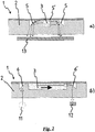
- Figure 1 shows a schematic representation of a measuring chip 1 according to the invention from above with a base plate 2 made of a transparent polymer material.
- Fluid channels 4 and 4 ′ for supplying and removing fluid are formed in the base plate 2.
- the direction of fluid flow is indicated by black arrows.
- the fluid channels 4, 4 ′ meet the longitudinal axis of the measuring cell 3 essentially perpendicularly, so that in the extension of the longitudinal axis of the measuring cell 3 there are planar wall surfaces for the introduction of excitation light.
- mirror surfaces 6 and 6 ' are arranged in the base plate for coupling and decoupling excitation light.
- the beam path of the excitation light is shown in the figures by open arrows.
- excitation light from a light source 11 which is provided in an operator device, is radiated essentially vertically from below into the base plate 3 and reflected by the mirror surface 6 and at an angle of 45 ° to the mirror surface in the direction of the longitudinal axis of the measuring cell 3 introduced into the measuring cell.
- Transmission light passing through the measuring cell 3 is reflected by the mirror surfaces 6 arranged on the opposite side and redirected at an angle of 45 ° towards the underside of the base plate 2, so that it is coupled out of the base plate 2 and onto a detector 12 which is provided in an operator device.
- mirror surfaces 5 are provided in the base plate, which reflectively emit emission light emitted by a fluid sample in the measuring cell, which emerges laterally from the measuring cell, to the underside of the base plate 2, where it is coupled out, and to a detector 13, which in FIG an operator device is provided.
- the Figures 2a) and 2b ) show schematic cross sections of the measuring chip according to Figure 1 along the lines AA and BB.
- the base plate 2 of the measuring chip 1 consists of transparent Polymer material.
- the mirror surfaces 5 on the side of the measuring cell 3 are shown in FIG Figure 2a ) and the mirror surfaces 6, 6 ', which are arranged in the extension of the longitudinal axis of the measuring cell 3 in the base plate, in Figure 2b ).
- the mirror surfaces 5, 6, 6 ' are formed by the interfaces between the transparent polymer material and a medium different from this, in this case air.
- corresponding recesses are provided in the base plate, which create an interface which is at an angle of 45 ° to the outlet walls of the measuring cell 3 or the base plate 2.
- Figure 2 shows that a further mirror surface 5 'is provided on the measuring chip on the upper side of the base plate Figure 1 is not shown.
- the mirror surface 5 ' is formed by a reflective cover film, for example a metal film. Emitted light that does not emerge from the fluid sample in the measuring cell 3 laterally from the measuring cell, but in Figure 2 upwards, is reflected back on the mirror surface 5 'formed by the cover film and either directed directly to the underside of the base plate 3 or to one of the mirror surfaces 5, where it is then deflected further towards the underside of the base plate 3.
- Figure 2a also shows a schematic representation of a detector 13 which is provided in an operator device and receives the light emitted by a fluid sample in the measuring cell 3 and which is coupled out downward from the base plate. In the operator device, the light received by the detector 13 is evaluated by appropriate electronics.
- Figure 2b also schematically shows a light source 11 provided in an operator device for the coupling of excitation light and a further detector 12 for the reception of transmission light.
- the mirror surfaces 5 shown are shown as several individual mirror surfaces (seven individual mirror surfaces on each side of the measuring cell). This type of mirror surface arrangement is suitable, for example, for carrying out a spatially resolved fluorescence measurement along the measurement section, for example for kinetic measurements.
- the mirror surfaces can be designed such that they direct the emission light emerging from the measuring cell along the longitudinal axis of the measuring cell to different detectors in an operator device or to a spatially resolving detector.
- the mirror surfaces 5 according to FIG Figure 1 be a continuous mirror surface on both sides of the measuring cell 3, so that as much of the emitted light as possible from the measuring cell 3 is directed onto a detector with or without spatial resolution.
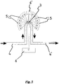
- Figure 3 shows an alternative embodiment of the measuring chip according to the invention, which is compared to the measuring chip of Figure 1 essentially differs by the design of the measuring cell 3 and the shape of the mirror surfaces 5.
- the top view of the measuring cell 3 is essentially circular with rounded side surfaces, and the mirror surfaces 5 are likewise designed in the shape of a segment of a circle around the measuring cell 3.
- the embodiment of the measuring chip according to the invention Figure 3 is suitable for all types of emission measurements and especially for angle-dependent scatter measurements.
- the mirror surfaces 5 are continuous mirror surfaces. For an angle-resolving measurement, several detectors or one spatially resolving detector are provided in the operator device.
- Figure 4 shows one according to the measuring cell Figure 3 Similar embodiment, but the mirror surfaces 5 are formed by individual, separate mirror surfaces.
- Figure 5 shows a schematic representation of a further alternative embodiment of the measuring chip according to the invention.
- the fluid channel 4, 4 takes a hairpin-shaped course in the base plate, and the apex of the hairpin-shaped course forms the measuring cell 3 of the measuring chip.
- Excitation light is introduced into the area of the measuring cell 3 via the mirror surfaces 6 and 6 ′, the light beam striking the portion of the fluid channel forming the measuring cell 3 laterally.
- Mirror surfaces 5 for deflecting and coupling out emission or scattered light are arranged in a circular segment around the section of the fluid channel forming the measuring cell 3.
- the measuring chip according to Figure 5 is suitable for all types of measurements, especially for angle-resolving scatter measurements.
- Figure 6 shows a schematic representation of a further embodiment of the measuring chip according to the invention, the area of the base plate comprising the measuring cell 3, the mirror surfaces 6 and 6 'for the deflection of the excitation light, the mirror surfaces 5 and the fluid channel 4' for the discharge of fluid, in the Basically like the measuring chip according to Figure 1 is trained.
- further fluid channels 4 "and 4"' are formed in the base plate, the fluid channel 4 "having two inlets and then winding as a mixing section and running in the base plate with several changes of direction.
- a further fluid channel 4"' can pass through the end of the mixing section another fluid can be added.
- This embodiment is intended to explain only by way of example how further elements can be provided in the base plate 2 of the measuring chip 1 according to the invention.
- the number of fluid channels, their shape and their course are to be adapted to the respective requirements of reactions, mixtures or other process steps to be carried out.
- reaction chambers and further fluid outlets can also be provided.
- Figure 7 shows variants of the mirror surfaces according to the invention for the deflection of emission or scattered light.
- Figure 7a shows one to Figure 2a ) Similar embodiment, but the mirror surfaces 5 are convexly curved for bundling light.
- Figure 7b shows a semicircular, convex mirror surface, which extends semicircularly around the measuring cell 3 with respect to the bottom surface of the base plate 2 and reflects light emitted or scattered from the measuring cell to the side and upwards.
- Figure 8 shows a further alternative embodiment of the measuring chip according to the invention for performing an angle-dependent scatter measurement in a perspective representation from above and in cross section from the side.
- Excitation light from a light source 11 in an operator device is coupled into the base plate 2 of the measuring chip 1 from the underside and deflected at a mirror surface 6 in the direction of the measuring cell 3.
- Light transmitted through the measuring cell is redirected on the opposite side of the measuring cell 3 by a mirror surface 6 'in the direction of the underside of the base plate 2 and decoupled from the measuring chip.
- Scattered light that emerges from the measuring cell 3 directly in the direction of the underside of the base plate 2 corresponds to a scattering angle of 90 ° and is received there by a detector 13 in an operator device below the base plate 2.
- the colloid content and the particle size distribution in a water sample can be determined from the ratio of the scattered light intensities at the scattering angles of 90 ° and 12 °.
Landscapes
- Chemical & Material Sciences (AREA)
- Health & Medical Sciences (AREA)
- General Health & Medical Sciences (AREA)
- Analytical Chemistry (AREA)
- Physics & Mathematics (AREA)
- Life Sciences & Earth Sciences (AREA)
- Biochemistry (AREA)
- General Physics & Mathematics (AREA)
- Immunology (AREA)
- Pathology (AREA)
- Hematology (AREA)
- Clinical Laboratory Science (AREA)
- Chemical Kinetics & Catalysis (AREA)
- Dispersion Chemistry (AREA)
- Nuclear Medicine, Radiotherapy & Molecular Imaging (AREA)
- Optical Measuring Cells (AREA)
- Investigating, Analyzing Materials By Fluorescence Or Luminescence (AREA)
Claims (11)
- Puce de mesure (1) servant à réaliser des mesures de l'émission et/ou de la dispersion de lumière à travers un échantillon de fluide dans un appareil d'opérateur, dans laquelle
la puce de mesure comporte une plaque de base (2) réalisée dans un matériau polymère transparent, et dans laquelle sont prévus dans la plaque de base (2) au moins une cellule de mesure (3) destinée à recevoir un échantillon de fluide et des canaux de fluide (4, 4') pour amener et évacuer du fluide vers et depuis la cellule de mesure (3), caractérisée en ce qu'est/sont prévue(s) dans la plaque de base (2), à l'extérieur de la cellule de mesure (3), une surface réfléchissante ou des surfaces réfléchissantes (5), qui est/sont disposée(s) dans la plaque de base (2) de façon telle que la lumière émise et/ou diffusée par un échantillon de fluide dans la cellule de mesure (3) est constamment réfléchie dans le matériau polymère de la plaque de base (2) et dirigée hors de la puce de mesure (13) en direction d'un détecteur de lumière prévu dans l'appareil d'opérateur. - Puce de mesure (1) selon la revendication 1, caractérisée en ce qu'est/que sont prévue(s) dans la plaque de base (2), à l'extérieur de la cellule de mesure (3), une autre surface réfléchissante ou d'autres surfaces réfléchissantes (6), qui est/sont disposée(s) de façon à diriger dans la cellule de mesure (3) la lumière d'excitation couplée dans la puce de mesure (1) par une source lumineuse (11) disposée à l'extérieur de la puce de mesure (1).
- Puce de mesure (1) selon l'une des revendications 1 ou 2, caractérisée en ce qu'est/que sont prévue(s) dans la plaque de base (2), à l'extérieur de la cellule de mesure (3), une autre surface réfléchissante ou d'autres surfaces réfléchissantes (6'), qui est/sont disposée(s) de façon à diriger hors de la puce de mesure (1) la lumière de transmission traversant la cellule de mesure, laquelle est couplée dans la puce de mesure (1) en tant que lumière d'excitation.
- Puce de mesure (1) selon l'une des revendications 2 ou 3, caractérisée en ce que l'autre surface réfléchissante ou les autres surfaces réfléchissantes (6, 6') sont disposées dans la plaque de base (2) de façon telle que la lumière réfléchie sur les surfaces réfléchissantes est constamment réfléchie dans le matériau polymère de la plaque de base (2).
- Puce de mesure selon l'une des revendications précédentes, caractérisée en ce que la cellule de mesure (3) présente, dans la direction d'écoulement du fluide, une section transversale rectangulaire ou carrée.
- Puce de mesure selon l'une des revendications précédentes, caractérisée en ce que la plaque de base (2) est réalisée en acrylate transparent, polyméthylacrylate, polyméthacrylate de méthyle, polycarbonate, polystyrène, polyimide, copolymère de cyclooléfine (COC), polymère de cyclooléfine (COP), polyuréthane, résine époxy, acrylate halogéné, polysiloxane deutérié, PDMS, polyimide fluoré, polyétherimide, perfluorocyclobutane, copolymère de perfluorovinyléther (téflon AF), cyclopolymère de perfluorovinyléther (CYTOP), polytétrafluoréthylène (PTFE), sulfure de polyaryléther fluoré (FRAESI), verre polymère inorganique, copolymère de polyméthacrylate de méthyle (P2ANS).
- Puce de mesure selon l'une des revendications précédentes, caractérisée en ce qu'au moins quelques-unes des surfaces réfléchissantes (5, 6, 6') sont conçues en tant qu'interfaces entre le matériau polymère transparent de la plaque de base (2) et un milieu gazeux ou liquide, de préférence un milieu gazeux et plus préférablement de l'air, et le matériau polymère, le milieu gazeux ou liquide et l'état de surface des interfaces réalisées en tant que surfaces réfléchissantes sont choisis de façon telle que les interfaces réalisées en tant que surfaces réfléchissantes sont totalement réfléchissantes au-dessous d'un angle d'incidence de la lumière prédéterminé, de préférence à un angle d'incidence de la lumière inférieur ou égal à 45° par rapport à la surface.
- Puce de mesure selon l'une des revendications précédentes, caractérisée en ce que la plaque de base (2) de la puce de mesure (1) présente une surface de fond plane ou planaire.
- Puce de mesure selon l'une des revendications précédentes, caractérisée en ce que les surfaces réfléchissantes (5, 6, 6') sont formées de manière plane ou planaire ou incurvée.
- Dispositif servant à réaliser des mesures de l'émission et/ou de la dispersion de lumière à travers un échantillon de fluide, caractérisé en ce que le dispositif comprend une puce de mesure (1) selon l'une des revendications précédentes et un appareil d'opérateur, l'appareil d'opérateur comportant un espace destiné à recevoir la puce de mesure (1) et au moins une source lumineuse (11) pour le couplage de la lumière dans la puce de mesure (1) et un détecteur ou plusieurs détecteurs (12, 13) permettant la détection de la lumière extraite de la puce de mesure (1).
- Dispositif selon la revendication 10, caractérisé en ce qu'est prévu dans l'appareil d'opérateur un détecteur à résolution spatiale (13) permettant la détection de la lumière d'émission ou de la lumière diffusée.
Applications Claiming Priority (2)
| Application Number | Priority Date | Filing Date | Title |
|---|---|---|---|
| DE102005062174A DE102005062174C5 (de) | 2005-12-23 | 2005-12-23 | Meßchip |
| PCT/EP2006/069501 WO2007074038A1 (fr) | 2005-12-23 | 2006-12-08 | Puce de mesure |
Publications (2)
| Publication Number | Publication Date |
|---|---|
| EP1963821A1 EP1963821A1 (fr) | 2008-09-03 |
| EP1963821B1 true EP1963821B1 (fr) | 2020-03-18 |
Family
ID=37730379
Family Applications (1)
| Application Number | Title | Priority Date | Filing Date |
|---|---|---|---|
| EP06841313.7A Active EP1963821B1 (fr) | 2005-12-23 | 2006-12-08 | Puce de mesure |
Country Status (4)
| Country | Link |
|---|---|
| US (1) | US7894071B2 (fr) |
| EP (1) | EP1963821B1 (fr) |
| DE (1) | DE102005062174C5 (fr) |
| WO (1) | WO2007074038A1 (fr) |
Families Citing this family (27)
| Publication number | Priority date | Publication date | Assignee | Title |
|---|---|---|---|---|
| EP2152417B1 (fr) | 2007-05-04 | 2018-07-11 | Opko Diagnostics, LLC | Dispositif et méthode pour analyses dans des systèmes microfluidiques |
| DE102008006035B3 (de) * | 2008-01-25 | 2009-06-18 | Fraunhofer-Gesellschaft zur Förderung der angewandten Forschung e.V. | Mikrotechnisches Bauelement zur Untersuchung einer fluidischen Probe und ein Verfahren zu dessen Herstellung |
| WO2011120006A1 (fr) * | 2010-03-25 | 2011-09-29 | Auantalife, Inc. A Delaware Corporation | Système de détection pour analyses à base de gouttelettes |
| US8576396B2 (en) * | 2008-11-19 | 2013-11-05 | Postnova Analytics Gmbh | Cell construction for light scatter detectors having self-focusing properties |
| DE102009000529A1 (de) | 2009-01-30 | 2010-08-19 | INSTITUT FüR MIKROTECHNIK MAINZ GMBH | Mikrofluidischer Chip mit Druckmesseinrichtung |
| ES2695039T3 (es) | 2009-02-02 | 2018-12-28 | Opko Diagnostics, Llc | Estructuras para controlar la interacción de luz con dispositivos microfluídicos |
| CA2716269A1 (fr) * | 2009-10-06 | 2011-04-06 | University Of Windsor | Methode et appareil pour l'analyse cinetique de la fonction plaquettaire dans des echantillons de sang total |
| ES2377908B1 (es) * | 2010-01-11 | 2013-02-13 | Consejo Superior De Investigaciones Científicas (Csic) | Dispositivo y sistema de contabilización y análisis de partículas y uso de dicho sistema. |
| DE102010001714A1 (de) * | 2010-02-09 | 2011-08-11 | Robert Bosch GmbH, 70469 | Vorrichtung und Verfahren zur optischen Parallelanalyse einer Probenanordnung und entsprechendes Herstellungsverfahren |
| DE102010013752A1 (de) | 2010-03-31 | 2011-10-06 | Roche Diagnostics Gmbh | Multifunktionelle Detektionsküvette |
| JP2012093190A (ja) * | 2010-10-26 | 2012-05-17 | Olympus Corp | 蛍光センサの補正方法おび蛍光センサ |
| CA2856353C (fr) * | 2011-12-02 | 2020-03-24 | Senseair Ab | Cellule a gaz epoxy moulee pour mesures optiques et procede de moulage |
| TWI596494B (zh) | 2012-03-05 | 2017-08-21 | Opko診斷法有限責任公司 | 預測前列腺癌風險及前列腺腺體體積之方法及裝置 |
| JP6169367B2 (ja) * | 2013-02-12 | 2017-07-26 | 新光電気工業株式会社 | 光学分析装置 |
| CN103824813B (zh) * | 2014-03-05 | 2016-05-11 | 陈龙 | 一种单片集成的微荧光分析系统及其制作方法 |
| JP6281945B2 (ja) * | 2014-03-11 | 2018-02-21 | 国立研究開発法人産業技術総合研究所 | 多孔質媒体を利用したアッセイ装置 |
| GB2530034B (en) * | 2014-09-09 | 2017-08-09 | Max-Planck-Gesellschaft Zur Forderung Der Wss E V | Particle detection apparatus |
| KR101638016B1 (ko) * | 2015-05-28 | 2016-07-08 | 광주과학기술원 | 내시경 |
| KR101766328B1 (ko) * | 2015-05-28 | 2017-08-08 | 광주과학기술원 | 현미경 |
| DE102015217700B3 (de) | 2015-09-16 | 2016-12-15 | Fraunhofer-Gesellschaft zur Förderung der angewandten Forschung e.V. | Verfahren zur Bestimmung des mittleren Trägheitsradius von Partikeln mit einer Größe von kleinergleich 200 nm in einer Suspension und Vorrichtung zur Durchführung des Verfahrens |
| JP6704920B2 (ja) * | 2015-10-14 | 2020-06-03 | アルプスアルパイン株式会社 | 流路構造体および測定対象液体の測定装置 |
| JP6549747B2 (ja) * | 2017-04-14 | 2019-07-24 | リオン株式会社 | 粒子測定装置および粒子測定方法 |
| WO2018200123A1 (fr) * | 2017-04-28 | 2018-11-01 | Becton, Dickinson And Company | Cartouches de détection de particules, systèmes associés et leurs procédés d'utilisation |
| US11249010B2 (en) * | 2019-03-28 | 2022-02-15 | Flir Detection, Inc. | Carbon filled polymer structure for high temperature chemical detector systems and methods |
| JP7553013B2 (ja) * | 2020-07-01 | 2024-09-18 | アルプスアルパイン株式会社 | 分析装置 |
| CN112683799A (zh) * | 2020-12-14 | 2021-04-20 | 武汉丰兴环保科技有限公司 | 一种水质在线一体式长光程模块 |
| DE102024208096A1 (de) * | 2024-08-26 | 2026-02-26 | Robert Bosch Gesellschaft mit beschränkter Haftung | Chiplabor-Kartusche zur Fluoreszenzanalyse mit integriertem Anregungsmittel |
Citations (1)
| Publication number | Priority date | Publication date | Assignee | Title |
|---|---|---|---|---|
| EP0488947A1 (fr) * | 1990-11-26 | 1992-06-03 | Ciba-Geigy Ag | Cellule détectrice |
Family Cites Families (25)
| Publication number | Priority date | Publication date | Assignee | Title |
|---|---|---|---|---|
| US4154233A (en) | 1977-08-11 | 1979-05-15 | Brown James E | Human support apparatus |
| NL7804144A (nl) * | 1978-04-18 | 1979-10-22 | Akzo Nv | Inrichting voor clorimetrische bepalingen. |
| US4273419A (en) * | 1980-03-21 | 1981-06-16 | The United States Of America As Represented By The Secretary Of The Air Force | Light-scattering disc collector |
| GB8509491D0 (en) | 1985-04-12 | 1985-05-15 | Plessey Co Plc | Optic waveguide biosensors |
| US5122284A (en) * | 1990-06-04 | 1992-06-16 | Abaxis, Inc. | Apparatus and method for optically analyzing biological fluids |
| US5439647A (en) * | 1994-02-25 | 1995-08-08 | Fiberchem, Inc. | Chip level waveguide sensor |
| US5489988A (en) * | 1995-01-03 | 1996-02-06 | Motorola | Environmental sensor and method therefor |
| US5858187A (en) * | 1996-09-26 | 1999-01-12 | Lockheed Martin Energy Systems, Inc. | Apparatus and method for performing electrodynamic focusing on a microchip |
| DE19647644C2 (de) * | 1996-11-18 | 1999-04-15 | Fraunhofer Ges Forschung | Mikromechanische Transmissionsmeßzelle |
| DE19731241C2 (de) * | 1997-07-21 | 1999-09-23 | Fraunhofer Ges Forschung | Vorrichtung und Verfahren zur Bestimmung von Fluidkomponenten und Verfahren zur Herstellung der Vorrichtung |
| US6100541A (en) * | 1998-02-24 | 2000-08-08 | Caliper Technologies Corporation | Microfluidic devices and systems incorporating integrated optical elements |
| CA2320296A1 (fr) * | 1998-05-18 | 1999-11-25 | University Of Washington | Cartouche d'analyse liquide |
| WO2000043552A2 (fr) * | 1999-01-25 | 2000-07-27 | Ut-Battelle, Llc | Biocapteurs mulitispectre et multifonctions, et leurs procedes d'utilisation |
| US6906797B1 (en) * | 1999-09-13 | 2005-06-14 | Aclara Biosciences, Inc. | Side light activated microfluid channels |
| DE10116674C2 (de) * | 2001-04-04 | 2003-08-14 | Eppendorf Ag | Vorrichtung zur Detektion von Fluiden in einem mikrofluidischen Bauteil |
| US7524459B2 (en) * | 2002-01-24 | 2009-04-28 | California Institute Of Technology In Pasadena | Optoelectronic and microfluidic integration for miniaturized spectroscopic devices |
| US6839140B1 (en) * | 2002-07-03 | 2005-01-04 | Los Gatos Research | Cavity-enhanced liquid absorption spectroscopy |
| JP2004069397A (ja) * | 2002-08-02 | 2004-03-04 | Nec Corp | 分析チップおよび分析装置 |
| DE10245845B4 (de) * | 2002-09-30 | 2006-06-29 | INSTITUT FüR MIKROTECHNIK MAINZ GMBH | Meßchip für die Verwendung ein einer Vorrichtung zur quantitativen Bestimmung eines Analyten in einer Probe und Vorrichtung mit diesem Meßchip |
| EP1494007B8 (fr) * | 2003-06-30 | 2014-09-24 | Tecan Trading AG | Dispositif et procédé pour l'analyse d'échantillons |
| US7221455B2 (en) * | 2004-01-20 | 2007-05-22 | The Regents Of The Unversity Of California | Integrated, fluorescence-detecting microanalytical system |
| DK1730518T3 (da) * | 2004-02-26 | 2009-11-16 | Delta Dansk Elektronik Lys & A | Fremgangsmåde, chip, anordning og integreret system til detektering af biologiske partikler |
| EP1752758A1 (fr) * | 2005-08-09 | 2007-02-14 | Roche Diagnostics GmbH | Détection photométrique dans le plan utilisant un disque rotatif |
| US7817698B2 (en) * | 2006-08-11 | 2010-10-19 | California Institute Of Technology | Mechanically tunable elastomeric optofluidic distributed feedback dye lasers |
| GB0624148D0 (en) * | 2006-12-02 | 2007-01-10 | Univ Teesside | Detection method |
-
2005
- 2005-12-23 DE DE102005062174A patent/DE102005062174C5/de not_active Expired - Fee Related
-
2006
- 2006-12-08 EP EP06841313.7A patent/EP1963821B1/fr active Active
- 2006-12-08 US US12/086,735 patent/US7894071B2/en not_active Expired - Fee Related
- 2006-12-08 WO PCT/EP2006/069501 patent/WO2007074038A1/fr not_active Ceased
Patent Citations (1)
| Publication number | Priority date | Publication date | Assignee | Title |
|---|---|---|---|---|
| EP0488947A1 (fr) * | 1990-11-26 | 1992-06-03 | Ciba-Geigy Ag | Cellule détectrice |
Also Published As
| Publication number | Publication date |
|---|---|
| US20090161108A1 (en) | 2009-06-25 |
| DE102005062174B3 (de) | 2007-05-31 |
| EP1963821A1 (fr) | 2008-09-03 |
| DE102005062174C5 (de) | 2010-05-06 |
| US7894071B2 (en) | 2011-02-22 |
| WO2007074038A1 (fr) | 2007-07-05 |
Similar Documents
| Publication | Publication Date | Title |
|---|---|---|
| EP1963821B1 (fr) | Puce de mesure | |
| EP0938660B1 (fr) | Cellule micromecanique de mesure de transmission | |
| DE19725050C2 (de) | Anordnung zur Detektion biochemischer oder chemischer Substanzen mittels Fluoreszenzlichtanregung und Verfahren zu deren Herstellung | |
| DE3876321T2 (de) | Kopf zur messung des reflexionsvermoegens von entfernten proben. | |
| DE19955556B4 (de) | Meßanordnung zum parallelen Auslesen von SPR-Sensoren | |
| DE102007033124B4 (de) | Vorrichtung zur optischen Detektion von Substanzen in einem flüssigen oder gasförmigen Medium | |
| EP0148497B1 (fr) | Dispositif pour conduire et collecter la lumière en photométrie | |
| DE202010018623U1 (de) | Strukturen zur Steuerung der Lichtwechselwirkung mit mikrofluidischen Vorrichtungen | |
| EP1257809A1 (fr) | Detecteur spr et dispositif de detection spr | |
| EP2652481A2 (fr) | Dispositif pour l'analyse photométrique ou spectrométrique d'un échantillon liquide | |
| AT513859B1 (de) | Mikro-Fluoreszenzdetektionsvorrichtung sowie Verfahren zur Detektion | |
| EP1347284B1 (fr) | Porte-échantillon avec optique intégrée | |
| WO2008135566A2 (fr) | Unité de mesure et procédé d'examen optique d'un liquide pour déterminer une concentration d'un analyte | |
| EP2088423A1 (fr) | Noyau de guide d'onde et biocapteur | |
| WO2003025553A2 (fr) | Appareil d'analyse permettant de determiner la structure chimique et/ou la composition d'une pluralite d'echantillons et porte-echantillons | |
| DE19647644C2 (de) | Mikromechanische Transmissionsmeßzelle | |
| DE102013215210B3 (de) | Reaktionsgefäß, Reaktionsgefäßanordnung und Verfahren zur Analyseeiner Substanz | |
| WO2004106901A1 (fr) | Agencement et procede pour la detection optique de molecules et/ou de particules chimiques, biochimiques contenues dans des echantillons | |
| DE102020201112A1 (de) | Optische Auslesung von Prozessen innerhalb einer mikrofluidischen Vorrichtung | |
| DE112021003493T5 (de) | Vorrichtung zur Bestimmung der Anwesenheit oder Konzentration von Zielmolekülen | |
| DE29824644U1 (de) | Vorrichtung zur Durchführung photometrischer Tests | |
| EP2765405A1 (fr) | Système de néphélométrie | |
| DE102016211471A1 (de) | Anordnung und Verfahren zur winkelaufgelösten Streulichtmessung mittels einer Wellenleiter-Sonde | |
| DE102016204755A1 (de) | Optische Messvorrichtung mit Gittersensor |
Legal Events
| Date | Code | Title | Description |
|---|---|---|---|
| PUAI | Public reference made under article 153(3) epc to a published international application that has entered the european phase |
Free format text: ORIGINAL CODE: 0009012 |
|
| 17P | Request for examination filed |
Effective date: 20080521 |
|
| AK | Designated contracting states |
Kind code of ref document: A1 Designated state(s): AT BE BG CH CY CZ DE DK EE ES FI FR GB GR HU IE IS IT LI LT LU LV MC NL PL PT RO SE SI SK TR |
|
| 17Q | First examination report despatched |
Effective date: 20090402 |
|
| DAX | Request for extension of the european patent (deleted) | ||
| RAP1 | Party data changed (applicant data changed or rights of an application transferred) |
Owner name: FRAUNHOFER-GESELLSCHAFT ZUR FOERDERUNG DER ANGEWAN |
|
| STAA | Information on the status of an ep patent application or granted ep patent |
Free format text: STATUS: EXAMINATION IS IN PROGRESS |
|
| REG | Reference to a national code |
Ref country code: DE Ref legal event code: R079 Ref document number: 502006016402 Country of ref document: DE Free format text: PREVIOUS MAIN CLASS: G01N0021030000 Ipc: G01N0021050000 |
|
| GRAP | Despatch of communication of intention to grant a patent |
Free format text: ORIGINAL CODE: EPIDOSNIGR1 |
|
| STAA | Information on the status of an ep patent application or granted ep patent |
Free format text: STATUS: GRANT OF PATENT IS INTENDED |
|
| RIC1 | Information provided on ipc code assigned before grant |
Ipc: G01N 21/53 20060101ALI20190906BHEP Ipc: G01N 21/03 20060101ALI20190906BHEP Ipc: B01L 3/00 20060101ALI20190906BHEP Ipc: G01N 21/05 20060101AFI20190906BHEP Ipc: G01N 21/64 20060101ALI20190906BHEP |
|
| INTG | Intention to grant announced |
Effective date: 20191011 |
|
| GRAS | Grant fee paid |
Free format text: ORIGINAL CODE: EPIDOSNIGR3 |
|
| GRAA | (expected) grant |
Free format text: ORIGINAL CODE: 0009210 |
|
| STAA | Information on the status of an ep patent application or granted ep patent |
Free format text: STATUS: THE PATENT HAS BEEN GRANTED |
|
| AK | Designated contracting states |
Kind code of ref document: B1 Designated state(s): AT BE BG CH CY CZ DE DK EE ES FI FR GB GR HU IE IS IT LI LT LU LV MC NL PL PT RO SE SI SK TR |
|
| REG | Reference to a national code |
Ref country code: GB Ref legal event code: FG4D Free format text: NOT ENGLISH |
|
| REG | Reference to a national code |
Ref country code: DE Ref legal event code: R096 Ref document number: 502006016402 Country of ref document: DE |
|
| REG | Reference to a national code |
Ref country code: AT Ref legal event code: REF Ref document number: 1246470 Country of ref document: AT Kind code of ref document: T Effective date: 20200415 Ref country code: IE Ref legal event code: FG4D Free format text: LANGUAGE OF EP DOCUMENT: GERMAN |
|
| PG25 | Lapsed in a contracting state [announced via postgrant information from national office to epo] |
Ref country code: FI Free format text: LAPSE BECAUSE OF FAILURE TO SUBMIT A TRANSLATION OF THE DESCRIPTION OR TO PAY THE FEE WITHIN THE PRESCRIBED TIME-LIMIT Effective date: 20200318 |
|
| REG | Reference to a national code |
Ref country code: NL Ref legal event code: MP Effective date: 20200318 |
|
| PG25 | Lapsed in a contracting state [announced via postgrant information from national office to epo] |
Ref country code: GR Free format text: LAPSE BECAUSE OF FAILURE TO SUBMIT A TRANSLATION OF THE DESCRIPTION OR TO PAY THE FEE WITHIN THE PRESCRIBED TIME-LIMIT Effective date: 20200619 Ref country code: BG Free format text: LAPSE BECAUSE OF FAILURE TO SUBMIT A TRANSLATION OF THE DESCRIPTION OR TO PAY THE FEE WITHIN THE PRESCRIBED TIME-LIMIT Effective date: 20200618 Ref country code: LV Free format text: LAPSE BECAUSE OF FAILURE TO SUBMIT A TRANSLATION OF THE DESCRIPTION OR TO PAY THE FEE WITHIN THE PRESCRIBED TIME-LIMIT Effective date: 20200318 Ref country code: SE Free format text: LAPSE BECAUSE OF FAILURE TO SUBMIT A TRANSLATION OF THE DESCRIPTION OR TO PAY THE FEE WITHIN THE PRESCRIBED TIME-LIMIT Effective date: 20200318 |
|
| REG | Reference to a national code |
Ref country code: LT Ref legal event code: MG4D |
|
| PG25 | Lapsed in a contracting state [announced via postgrant information from national office to epo] |
Ref country code: NL Free format text: LAPSE BECAUSE OF FAILURE TO SUBMIT A TRANSLATION OF THE DESCRIPTION OR TO PAY THE FEE WITHIN THE PRESCRIBED TIME-LIMIT Effective date: 20200318 |
|
| PG25 | Lapsed in a contracting state [announced via postgrant information from national office to epo] |
Ref country code: RO Free format text: LAPSE BECAUSE OF FAILURE TO SUBMIT A TRANSLATION OF THE DESCRIPTION OR TO PAY THE FEE WITHIN THE PRESCRIBED TIME-LIMIT Effective date: 20200318 Ref country code: LT Free format text: LAPSE BECAUSE OF FAILURE TO SUBMIT A TRANSLATION OF THE DESCRIPTION OR TO PAY THE FEE WITHIN THE PRESCRIBED TIME-LIMIT Effective date: 20200318 Ref country code: PT Free format text: LAPSE BECAUSE OF FAILURE TO SUBMIT A TRANSLATION OF THE DESCRIPTION OR TO PAY THE FEE WITHIN THE PRESCRIBED TIME-LIMIT Effective date: 20200812 Ref country code: CZ Free format text: LAPSE BECAUSE OF FAILURE TO SUBMIT A TRANSLATION OF THE DESCRIPTION OR TO PAY THE FEE WITHIN THE PRESCRIBED TIME-LIMIT Effective date: 20200318 Ref country code: SK Free format text: LAPSE BECAUSE OF FAILURE TO SUBMIT A TRANSLATION OF THE DESCRIPTION OR TO PAY THE FEE WITHIN THE PRESCRIBED TIME-LIMIT Effective date: 20200318 Ref country code: IS Free format text: LAPSE BECAUSE OF FAILURE TO SUBMIT A TRANSLATION OF THE DESCRIPTION OR TO PAY THE FEE WITHIN THE PRESCRIBED TIME-LIMIT Effective date: 20200718 Ref country code: EE Free format text: LAPSE BECAUSE OF FAILURE TO SUBMIT A TRANSLATION OF THE DESCRIPTION OR TO PAY THE FEE WITHIN THE PRESCRIBED TIME-LIMIT Effective date: 20200318 |
|
| REG | Reference to a national code |
Ref country code: DE Ref legal event code: R097 Ref document number: 502006016402 Country of ref document: DE |
|
| PLBE | No opposition filed within time limit |
Free format text: ORIGINAL CODE: 0009261 |
|
| STAA | Information on the status of an ep patent application or granted ep patent |
Free format text: STATUS: NO OPPOSITION FILED WITHIN TIME LIMIT |
|
| PG25 | Lapsed in a contracting state [announced via postgrant information from national office to epo] |
Ref country code: ES Free format text: LAPSE BECAUSE OF FAILURE TO SUBMIT A TRANSLATION OF THE DESCRIPTION OR TO PAY THE FEE WITHIN THE PRESCRIBED TIME-LIMIT Effective date: 20200318 Ref country code: IT Free format text: LAPSE BECAUSE OF FAILURE TO SUBMIT A TRANSLATION OF THE DESCRIPTION OR TO PAY THE FEE WITHIN THE PRESCRIBED TIME-LIMIT Effective date: 20200318 Ref country code: DK Free format text: LAPSE BECAUSE OF FAILURE TO SUBMIT A TRANSLATION OF THE DESCRIPTION OR TO PAY THE FEE WITHIN THE PRESCRIBED TIME-LIMIT Effective date: 20200318 |
|
| 26N | No opposition filed |
Effective date: 20201221 |
|
| PG25 | Lapsed in a contracting state [announced via postgrant information from national office to epo] |
Ref country code: PL Free format text: LAPSE BECAUSE OF FAILURE TO SUBMIT A TRANSLATION OF THE DESCRIPTION OR TO PAY THE FEE WITHIN THE PRESCRIBED TIME-LIMIT Effective date: 20200318 |
|
| PG25 | Lapsed in a contracting state [announced via postgrant information from national office to epo] |
Ref country code: SI Free format text: LAPSE BECAUSE OF FAILURE TO SUBMIT A TRANSLATION OF THE DESCRIPTION OR TO PAY THE FEE WITHIN THE PRESCRIBED TIME-LIMIT Effective date: 20200318 |
|
| PG25 | Lapsed in a contracting state [announced via postgrant information from national office to epo] |
Ref country code: MC Free format text: LAPSE BECAUSE OF FAILURE TO SUBMIT A TRANSLATION OF THE DESCRIPTION OR TO PAY THE FEE WITHIN THE PRESCRIBED TIME-LIMIT Effective date: 20200318 |
|
| REG | Reference to a national code |
Ref country code: BE Ref legal event code: MM Effective date: 20201231 |
|
| PG25 | Lapsed in a contracting state [announced via postgrant information from national office to epo] |
Ref country code: LU Free format text: LAPSE BECAUSE OF NON-PAYMENT OF DUE FEES Effective date: 20201208 Ref country code: IE Free format text: LAPSE BECAUSE OF NON-PAYMENT OF DUE FEES Effective date: 20201208 |
|
| REG | Reference to a national code |
Ref country code: AT Ref legal event code: MM01 Ref document number: 1246470 Country of ref document: AT Kind code of ref document: T Effective date: 20201208 |
|
| PG25 | Lapsed in a contracting state [announced via postgrant information from national office to epo] |
Ref country code: AT Free format text: LAPSE BECAUSE OF NON-PAYMENT OF DUE FEES Effective date: 20201208 |
|
| PG25 | Lapsed in a contracting state [announced via postgrant information from national office to epo] |
Ref country code: TR Free format text: LAPSE BECAUSE OF FAILURE TO SUBMIT A TRANSLATION OF THE DESCRIPTION OR TO PAY THE FEE WITHIN THE PRESCRIBED TIME-LIMIT Effective date: 20200318 Ref country code: CY Free format text: LAPSE BECAUSE OF FAILURE TO SUBMIT A TRANSLATION OF THE DESCRIPTION OR TO PAY THE FEE WITHIN THE PRESCRIBED TIME-LIMIT Effective date: 20200318 |
|
| PG25 | Lapsed in a contracting state [announced via postgrant information from national office to epo] |
Ref country code: BE Free format text: LAPSE BECAUSE OF NON-PAYMENT OF DUE FEES Effective date: 20201231 |
|
| P01 | Opt-out of the competence of the unified patent court (upc) registered |
Effective date: 20230524 |
|
| PGFP | Annual fee paid to national office [announced via postgrant information from national office to epo] |
Ref country code: GB Payment date: 20231220 Year of fee payment: 18 |
|
| PGFP | Annual fee paid to national office [announced via postgrant information from national office to epo] |
Ref country code: FR Payment date: 20231220 Year of fee payment: 18 |
|
| PGFP | Annual fee paid to national office [announced via postgrant information from national office to epo] |
Ref country code: CH Payment date: 20240109 Year of fee payment: 18 |
|
| REG | Reference to a national code |
Ref country code: CH Ref legal event code: PL |
|
| GBPC | Gb: european patent ceased through non-payment of renewal fee |
Effective date: 20241208 |
|
| PG25 | Lapsed in a contracting state [announced via postgrant information from national office to epo] |
Ref country code: GB Free format text: LAPSE BECAUSE OF NON-PAYMENT OF DUE FEES Effective date: 20241208 |
|
| PG25 | Lapsed in a contracting state [announced via postgrant information from national office to epo] |
Ref country code: FR Free format text: LAPSE BECAUSE OF NON-PAYMENT OF DUE FEES Effective date: 20241231 |
|
| PG25 | Lapsed in a contracting state [announced via postgrant information from national office to epo] |
Ref country code: CH Free format text: LAPSE BECAUSE OF NON-PAYMENT OF DUE FEES Effective date: 20241231 |
|
| PGFP | Annual fee paid to national office [announced via postgrant information from national office to epo] |
Ref country code: DE Payment date: 20251222 Year of fee payment: 20 |