EP1973189A1 - Mikrostrukturen einer koaxialen Übertragungsleitung und Herstellungsverfahren dafür - Google Patents
Mikrostrukturen einer koaxialen Übertragungsleitung und Herstellungsverfahren dafür Download PDFInfo
- Publication number
- EP1973189A1 EP1973189A1 EP08153138A EP08153138A EP1973189A1 EP 1973189 A1 EP1973189 A1 EP 1973189A1 EP 08153138 A EP08153138 A EP 08153138A EP 08153138 A EP08153138 A EP 08153138A EP 1973189 A1 EP1973189 A1 EP 1973189A1
- Authority
- EP
- European Patent Office
- Prior art keywords
- transmission line
- center conductor
- coaxial transmission
- microstructure
- outer conductor
- Prior art date
- Legal status (The legal status is an assumption and is not a legal conclusion. Google has not performed a legal analysis and makes no representation as to the accuracy of the status listed.)
- Granted
Links
Images





Classifications
-
- H—ELECTRICITY
- H01—ELECTRIC ELEMENTS
- H01P—WAVEGUIDES; RESONATORS, LINES, OR OTHER DEVICES OF THE WAVEGUIDE TYPE
- H01P1/00—Auxiliary devices
- H01P1/04—Fixed joints
- H01P1/045—Coaxial joints
-
- H—ELECTRICITY
- H01—ELECTRIC ELEMENTS
- H01P—WAVEGUIDES; RESONATORS, LINES, OR OTHER DEVICES OF THE WAVEGUIDE TYPE
- H01P11/00—Apparatus or processes specially adapted for manufacturing waveguides or resonators, lines, or other devices of the waveguide type
- H01P11/001—Manufacturing waveguides or transmission lines of the waveguide type
- H01P11/005—Manufacturing coaxial lines
-
- H—ELECTRICITY
- H01—ELECTRIC ELEMENTS
- H01P—WAVEGUIDES; RESONATORS, LINES, OR OTHER DEVICES OF THE WAVEGUIDE TYPE
- H01P3/00—Waveguides; Transmission lines of the waveguide type
- H01P3/02—Waveguides; Transmission lines of the waveguide type with two longitudinal conductors
- H01P3/06—Coaxial lines
-
- H—ELECTRICITY
- H01—ELECTRIC ELEMENTS
- H01P—WAVEGUIDES; RESONATORS, LINES, OR OTHER DEVICES OF THE WAVEGUIDE TYPE
- H01P5/00—Coupling devices of the waveguide type
- H01P5/02—Coupling devices of the waveguide type with invariable factor of coupling
- H01P5/022—Transitions between lines of the same kind and shape, but with different dimensions
- H01P5/026—Transitions between lines of the same kind and shape, but with different dimensions between coaxial lines
-
- Y—GENERAL TAGGING OF NEW TECHNOLOGICAL DEVELOPMENTS; GENERAL TAGGING OF CROSS-SECTIONAL TECHNOLOGIES SPANNING OVER SEVERAL SECTIONS OF THE IPC; TECHNICAL SUBJECTS COVERED BY FORMER USPC CROSS-REFERENCE ART COLLECTIONS [XRACs] AND DIGESTS
- Y10—TECHNICAL SUBJECTS COVERED BY FORMER USPC
- Y10T—TECHNICAL SUBJECTS COVERED BY FORMER US CLASSIFICATION
- Y10T29/00—Metal working
- Y10T29/49—Method of mechanical manufacture
- Y10T29/49002—Electrical device making
- Y10T29/49016—Antenna or wave energy "plumbing" making
-
- Y—GENERAL TAGGING OF NEW TECHNOLOGICAL DEVELOPMENTS; GENERAL TAGGING OF CROSS-SECTIONAL TECHNOLOGIES SPANNING OVER SEVERAL SECTIONS OF THE IPC; TECHNICAL SUBJECTS COVERED BY FORMER USPC CROSS-REFERENCE ART COLLECTIONS [XRACs] AND DIGESTS
- Y10—TECHNICAL SUBJECTS COVERED BY FORMER USPC
- Y10T—TECHNICAL SUBJECTS COVERED BY FORMER US CLASSIFICATION
- Y10T29/00—Metal working
- Y10T29/49—Method of mechanical manufacture
- Y10T29/49002—Electrical device making
- Y10T29/49117—Conductor or circuit manufacturing
- Y10T29/49123—Co-axial cable
Definitions
- This invention relates generally to microfabrication technology and, more specifically, to coaxial transmission line microstructures and to methods of forming such microstructures using a sequential build process.
- the invention has particular applicability to devices for transmitting electromagnetic energy and other electronic signals.
- the formation of three-dimensional microstructures by sequential build processes has been described, for example, in U.S. Patent No. 7,012,489, to Sherrer et al (the '489 patent).
- The'489 patent discloses a coaxial transmission line microstructure formed by a sequential build process.
- the microstructure is formed on a substrate and includes an outer conductor, a center conductor and one or more dielectric support members which support the center conductor.
- the volume between the inner and outer conductors is gaseous or vacuous, formed by removal of a sacrificial material from the structure which previously filled such volume.
- the transmission line may, for example, be connected to a radio frequency (RF) or direct current (DC) cable, which in turn may be connected to another RF or DC cable, an RF module, an RF or DC source, a sub-system, a system and the like.
- RF should be understood to mean any frequency being propagated, specifically including microwave and millimeter wave frequencies.
- the process of connecting an external element to a coaxial transmission line microstructure is fraught with problems.
- the microstructures and standard connector terminations differ significantly in size.
- the inner diameter of the outer conductor and outer diameter of the center conductor of a coaxial transmission line microstructure are typically on the order of 100 to 1000 microns and 25 to 400 microns, respectively.
- the inner diameter of the outer conductor of a standard connector such as a 3.5mm, 2.4mm, 1 mm, GPPO, SMA, K, or W connector is generally on the order of 1 mm or more, with the outer diameter of the inner conductor being determined by the impedance of the connector.
- microfabricated coaxial transmission lines have dimensions that may be from two to more then ten times smaller than the smallest of these standard connectors. Given the rather large difference in size between the microstructure and connector, a simple joining of the two structures is not possible. Such a junction typically produces attenuation, radiation, and reflection of the propagating waves to a degree that is not acceptable for most applications .
- a microfabricated transition structure allowing mechanical joining of the two structures while preserving the desired transmission properties, such as low insertion loss and low return reflections over the operating frequencies would thus be desired.
- microstructure connectivity is the relatively delicate nature of the microstructures when considering the forces typically exerted on such connectors.
- the microstructures are formed from a number of relatively thin layers, with the center conductor being suspended in a gaseous or vacuous core volume within the outer conductor.
- periodic dielectric members are provided in the described microstructures to support the center conductor along its length, the microstructures are still susceptible to breakage and failure caused by excessive mechanical stresses. Such stresses would be expected to result from external forces applied to the microstructures during connection with large external components such as repeated mating with standard connectors.
- coaxial transmission line microstructures formed by a sequential build process.
- the microstructures include: a center conductor; an outer conductor disposed around the center conductor; a non-solid volume between the center conductor and the outer conductor; and a transition structure for transitioning between the coaxial transmission line and an electrical connector.
- the transition structure may include an end portion of the center conductor, wherein the end portion has an increased dimension along an axis thereof, and an enlarged region of the outer conductor adapted to attach to the electrical connector, the end portion of the center conductor being disposed in the enlarged region of the outer conductor.
- the non-solid volume is typically vacuum, air or other gas.
- the coaxial transmission line microstructure is typically formed over a substrate which may form part of the microstructure.
- the microstructure may be removed from a substrate on which it is formed. Such removed microstructure may be disposed on a different substrate.
- the coaxial transmission line microstructure may further include a support member in contact with the end portion of the center conductor for supporting the end portion.
- the support member may be formed of or include a dielectric material.
- the support member may be formed of a metal pedestal electrically isolating the center conductor and outer conductor by one or more intervening dielectric layers.
- the support member may take the form of a pedestal disposed beneath the end portion of the center conductor. At least a portion of the coaxial transmission line may have a rectangular coaxial (rectacoax) structure.
- connectorized coaxial transmission line microstructures are provided. Such microstructures include a coaxial transmission line microstructure as described above, and an electric connector connected to the center conductor and the outer conductor.
- the connectorized microstructures may further include a rigid member to which the connector is attached.
- a coaxial transmission line microstructure In accordance with a further aspect of the invention, provided are methods of forming a coaxial transmission line microstructure.
- the methods include: disposing a plurality of layers over a substrate, wherein the layers comprise one or more of dielectric, conductive and sacrificial materials; and forming from the layers a center conductor, an outer conductor disposed around the center conductor, a non-solid volume between the center conductor and the outer conductor and a transition structure for transitioning between the coaxial transmission line and an electric connector.
- the sequential build process is generally accomplished through processes including various combinations of: (a) metal, sacrificial material (e.g., photoresist) and dielectric coating processes; (b) surface planarization; (c) photolithography; and (d) etching or planarization or other removal processes.
- metal e.g., sacrificial material
- surface planarization e.g., photoresist
- photolithography e.g., photolithography
- etching or planarization or other removal processes e.g., etching or planarization or other removal processes.
- plating techniques are particularly useful, although other metal deposition techniques such as physical vapor deposition (PVD), screen printing and chemical vapor deposition (CVD) techniques may be used, the choice dependent on the dimensions of the coaxial structures, and the materials deployed.
- PVD physical vapor deposition
- CVD chemical vapor deposition
- microdevices such as in pressure sensors, rollover sensors, mass spectrometers, filters, microfluidic devices, heat sinks, hermetic packages, surgical instruments, blood pressure sensors, air flow sensors, hearing aid sensors, micromechanical sensors, image stabilizers, altitude sensors and autofocus sensors.
- the invention can be used as a general method for fabricating transitions between microstructural elements for transmission of electric and/or electromagnetic signals and power with external components through a connector, for example, a microwave connector.
- the exemplified coaxial transmission line microstructures and related waveguides are useful for propagation of electromagnetic energy having a frequency, for example, of from several MHz to 200 GHz or more, including radio frequency waves, millimeter waves and microwaves.
- the described transmission lines find further use in providing a simultaneous DC or lower frequency voltage, for example, in providing a bias to integrated or attached semiconductor devices.
- FIG. 1A-1C illustrates side-sectional, top-sectional and perspective views, respectively, of an exemplary coaxial transmission line microstructure 2 with a transition structure 4 and electric and/or electromagnetic connector (hereafter, electrical connector or connector) 6 in accordance with one aspect of the invention.
- the exemplified microstructure 2 is formed by a sequential build process, and includes a substrate 8, a center conductor 10, an outer conductor 12 disposed around and coaxial with the center conductor and one or more dielectric support members 14a, 14b for supporting the center conductor.
- the outer conductor 12 includes a conductive base layer 16 forming a lower wall, plural conductive layers forming the sidewalls, and conductive layer 24 forming an upper wall of the outer conductor.
- the conductive layers forming the lower wall 16 and upper wall 24 may optionally be provided as part of a conductive substrate or a conductive layer on a substrate.
- the volume 26 between the center conductor and the outer conductor is a non-solid, for example, a gas such as air or sulphur hexafluoride, vacuous or a liquid.
- the non-solid volume may be of a porous material such as a porous dielectric material formed, for example, from a dielectric material containing volatile porogens which may be removed with heating.
- the transition structure 4 of the microstructure 2 provides a larger geometry and lends mechanical support to the microstructure allowing for coupling to an electrical connector 6 without damaging the microstructure.
- the transition additionally minimizes or eliminates unwanted signal reflection between the transmission line microstructure 2 and electrical connector 6.
- the connector 6 has a coaxial conductor structure including a center conductor 28 and an outer conductor 30.
- the illustrated connector has a uniform geometry throughout its height.
- the connector is to be joined to the microstructure 2 at a first end 32 and to a mating connector connected to an external element (not shown), such as an RF or DC cable, which in turn may be connected to another such cable, an RF module, an RF or DC source, a sub-system, a system or the like, at a second end 34.
- Suitable connectors include, for example, surface mount technology (SMT) versions of connectors such as 1 mm, 2.4 mm, 3.5 mm, SMA, K, W, GPO and GPPO connectors, and other standard connectors such as those designed to mate to coplanar waveguides.
- SMT surface mount technology
- One or more solder layers 39 or other conductive bonding agent may be disposed on the center and outer conductor in the transition structure to allow bonding with the connector.
- the height of the center conductor mating surface 40 is equal to that of the mating surface 42 of the outer conductor in the transition region.
- the upper wall 24 of the outer conductor transition structure is open, thereby exposing the center conductor end portion 36.
- the center conductor is suspended in the transition structure with a support structure.
- the load of the transmission line in the transition structure can be significantly greater than that in other regions of the transmission line.
- the design of a suitable support structure for the center conductor end portion 36 will generally differ from that of the dielectric support members 14a used in the main regions of the transmission line.
- the design of the support structure for the end portion 36 may take various forms and will depend on the mechanical loads and stresses as a result of its mass and environment, as well as the added mechanical forces it may be subject to as a result of the attachment and use of the connector structure, particularly those associated with the center conductor 28.
- the support structure for the end portion takes the form of plural dielectric straps 14b.
- the dielectric straps as illustrated extend across the diameter of the outer conductor in the transition structure and are arranged in a spoke pattern.
- the straps 14b are embedded in the outer conductor 38. While the straps as illustrated extend below the center conductor end portion 36, it should be clear that they may be embedded in the end portion 36.
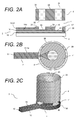
- FIG. 2A-2C shows side-sectional, top-sectional and perspective views of a further exemplary coaxial transmission line microstructure. Except as otherwise described, the description with respect to the exemplary structures of FIG. 1 is generally applicable to the structures shown in FIG. 2 , as well as the additional exemplary structures to be described.
- the support structure takes the form of a dielectric sheet 41 which supports the end portion 36 from below. As shown, the dielectric sheet 41 can be disposed across the entire transition structure or, alternatively, over a portion thereof.
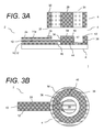
- FIG. 3A-B illustrates in side- and top-sectional views an exemplary such support structure which includes a support pedestal 42 disposed below and in supporting contact with the center conductor end portion.
- the pedestal is formed at least in part from a dielectric material layer 44 so as to electrically isolate the center conductor from the outer conductor and substrate.
- the support structure includes a dielectric material 44, formed on the substrate or optionally on the lower wall of the transition outer conductor for electrical isolation of the center conductor 10 from the substrate 8.
- the exemplified structure includes a dielectric layer 44 such as a silicon nitride or silicon oxide layer on the substrate 8 surface.
- An opening 46 in the base layer 16 of the outer conductor may be provided in the transition structure to reduce capacitive coupling of the center and outer conductors.
- the pedestal 42 is built up to a height such that the center conductor end portion 36 is directly supported thereby.
- the pedestal may include one or more additional layers of the same or a different material, including dielectric and/or conductive materials.
- a conductive layer 47 of the same material as the outer conductor is provided over the dielectric layer 44.
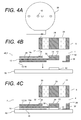
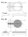
- the coaxial transmission line microstructure may be released from the substrate on which it is formed.
- the released microstructure 48 may be joined to a separate substrate 50 on which is provided one or more support pedestals 42 for supporting the center conductor end portion 36 of the released microstructure.
- the connector 6 may then be connected to the pedestal-supported microstructure.
- the support pedestals 42 may take the form, for example, of a printed circuit board, a ceramic, or a semiconductor, such as silicon, the post being formed on or as a part of the surface of the substrate 50 which itself may be of the same material. In this case, the pedestal 42 may be formed by machining or etching the substrate 50 surface.
- the support pedestal may be formed from a dielectric material, for example, a photoimageable dielectric material such as photosensitive-benzocyclobutene (Photo-BCB) resins such as those sold under the tradename Cyclotene (Dow Chemical Co.) and SU-8 resist (MicroChem Corp.).
- a photoimageable dielectric material such as photosensitive-benzocyclobutene (Photo-BCB) resins such as those sold under the tradename Cyclotene (Dow Chemical Co.) and SU-8 resist (MicroChem Corp.).
- Photo-BCB photosensitive-benzocyclobutene
- the support pedestals 42 may be formed and adhered to the released structure 48 rather than formed on the substrate 50.
- the thickness of the base layer 16 is selected to provide mechanical stability to the microstructure and to provide sufficient conductivity of the transmission line to provide sufficiently low loss. At microwave frequencies and beyond, structural influences become more pronounced, as the skin depth will typically be less than 1 ⁇ m. The thickness thus will depend, for example, on the specific base layer material, the particular frequency to be propagated and the intended application. In instances in which the final structure is to be removed from the substrate, it may be beneficial to employ a relatively thick base layer, for example, from about 20 to 150 ⁇ m or from 20 to 80 ⁇ m, for structural integrity. Where the final structure is to remain intact with the substrate, it may be desired to employ a relatively thin base layer which may be determined by the skin depth requirements of the frequencies used.
- a released microstructure with connectors can offer other advantages, such as smaller thickness profiles, application of the completed microstructure to separately made die or wafers of active devices, and connectorization of both opposing surfaces of the microstructure.
- Release of the structure from the substrate may be accomplished by various techniques, for example, by use of a sacrificial layer between the substrate and the base layer which can be removed upon completion of the structure in a suitable solvent or etchant that does not attack or is sufficiently selective to the structural materials chosen.
- Suitable materials for the sacrificial layer include, for example, photoresists, selectively etchable metals such as chrome or titanium, high temperature waxes, and various salts.
- a plurality of transmission lines as described above may be formed in a stacked arrangement, with the understanding that the transition structure would typically be disposed so that the connector structure can make electrical contact with the transition structure.
- the stacked arrangement can be achieved by continuation of the sequential build process through each stack, or by preforming the transmission lines on individual substrates, separating transmission line structures from their respective substrates using a release layer, and stacking the structures.
- Such stacked structures can be joined by thin layers of solders or conductive adhesives.
Landscapes
- Engineering & Computer Science (AREA)
- Manufacturing & Machinery (AREA)
- Waveguides (AREA)
- Multi-Conductor Connections (AREA)
Applications Claiming Priority (1)
| Application Number | Priority Date | Filing Date | Title |
|---|---|---|---|
| US91912407P | 2007-03-20 | 2007-03-20 |
Publications (2)
| Publication Number | Publication Date |
|---|---|
| EP1973189A1 true EP1973189A1 (de) | 2008-09-24 |
| EP1973189B1 EP1973189B1 (de) | 2012-12-05 |
Family
ID=39563288
Family Applications (1)
| Application Number | Title | Priority Date | Filing Date |
|---|---|---|---|
| EP08153138A Ceased EP1973189B1 (de) | 2007-03-20 | 2008-03-20 | Mikrostrukturen einer koaxialen Übertragungsleitung und Herstellungsverfahren dafür |
Country Status (4)
| Country | Link |
|---|---|
| US (6) | US7898356B2 (de) |
| EP (1) | EP1973189B1 (de) |
| JP (1) | JP2009005335A (de) |
| KR (1) | KR101472134B1 (de) |
Cited By (2)
| Publication number | Priority date | Publication date | Assignee | Title |
|---|---|---|---|---|
| CN110449332A (zh) * | 2019-08-13 | 2019-11-15 | 上海金铎禹辰水环境工程有限公司 | 一种复合结构金刚石薄膜及其制备方法 |
| SE2130283A1 (en) * | 2021-10-21 | 2023-04-22 | Gapwaves Ab | A coaxial transition arrangement |
Families Citing this family (74)
| Publication number | Priority date | Publication date | Assignee | Title |
|---|---|---|---|---|
| US9614266B2 (en) * | 2001-12-03 | 2017-04-04 | Microfabrica Inc. | Miniature RF and microwave components and methods for fabricating such components |
| ATE475999T1 (de) | 2003-03-04 | 2010-08-15 | Rohm & Haas Elect Mat | Koaxiale wellenleitermikrostrukturen und verfahern zu ihrer bildung |
| JP2008188755A (ja) | 2006-12-30 | 2008-08-21 | Rohm & Haas Electronic Materials Llc | 三次元微細構造体およびその形成方法 |
| EP1973189B1 (de) | 2007-03-20 | 2012-12-05 | Nuvotronics, LLC | Mikrostrukturen einer koaxialen Übertragungsleitung und Herstellungsverfahren dafür |
| EP1973190A1 (de) | 2007-03-20 | 2008-09-24 | Rohm and Haas Electronic Materials LLC | Integrierte elektronische Komponenten und Herstellungsverfahren dafür |
| TWI360912B (en) * | 2008-04-25 | 2012-03-21 | Univ Nat Chiao Tung | Vertical transition structure |
| US8659371B2 (en) * | 2009-03-03 | 2014-02-25 | Bae Systems Information And Electronic Systems Integration Inc. | Three-dimensional matrix structure for defining a coaxial transmission line channel |
| US20110123783A1 (en) | 2009-11-23 | 2011-05-26 | David Sherrer | Multilayer build processses and devices thereof |
| KR101917052B1 (ko) | 2010-01-22 | 2019-01-30 | 누보트로닉스, 인크. | 열관리 |
| US8917150B2 (en) | 2010-01-22 | 2014-12-23 | Nuvotronics, Llc | Waveguide balun having waveguide structures disposed over a ground plane and having probes located in channels |
| US8616908B2 (en) * | 2010-03-03 | 2013-12-31 | Thomas & Betts International, Inc. | Electrical connector with a cap with a sacrificial conductor |
| US8172596B2 (en) * | 2010-03-03 | 2012-05-08 | Thomas & Betts International, Inc. | Electrical connector with sacrificial appendage |
| US8597040B2 (en) * | 2010-03-03 | 2013-12-03 | Thomas & Betts International, Inc. | Device having an electrical connector and a sacrificial cap |
| DE102010019447A1 (de) * | 2010-05-05 | 2011-11-10 | Eos Gmbh Electro Optical Systems | Verfahren zum generativen Herstellen eines dreidimensionalen Objekts mit Räumelementen und Verfahren zum Erstellen eines entsprechenden Datensatzes |
| WO2012003506A2 (en) | 2010-07-02 | 2012-01-05 | Nuvotronics, Llc | Three-dimensional microstructures |
| JP5248578B2 (ja) * | 2010-11-19 | 2013-07-31 | 株式会社東芝 | 同軸コネクタ、同軸コネクタを有する基板、同軸コネクタを有する基板の製造方法、及び同軸コネクタ結合体 |
| US9200883B2 (en) * | 2011-05-05 | 2015-12-01 | International Business Machines Corporation | Transferable probe tips |
| US8866300B1 (en) | 2011-06-05 | 2014-10-21 | Nuvotronics, Llc | Devices and methods for solder flow control in three-dimensional microstructures |
| US8814601B1 (en) | 2011-06-06 | 2014-08-26 | Nuvotronics, Llc | Batch fabricated microconnectors |
| JP6335782B2 (ja) | 2011-07-13 | 2018-05-30 | ヌボトロニクス、インク. | 電子的および機械的な構造を製作する方法 |
| US9142497B2 (en) | 2011-10-05 | 2015-09-22 | Harris Corporation | Method for making electrical structure with air dielectric and related electrical structures |
| US9065163B1 (en) | 2011-12-23 | 2015-06-23 | Nuvotronics, Llc | High frequency power combiner/divider |
| CN103733427B (zh) * | 2012-02-03 | 2015-08-26 | 株式会社村田制作所 | 高频信号传输线路及电子设备 |
| GB2512982B (en) * | 2012-02-03 | 2018-06-13 | Murata Manufacturing Co | High-frequency signal transmission line and electronic device |
| US8952770B2 (en) * | 2012-06-21 | 2015-02-10 | Oml, Inc. | Self keying and orientation system for a repeatable waveguide calibration and connection |
| US9165723B2 (en) * | 2012-08-23 | 2015-10-20 | Harris Corporation | Switches for use in microelectromechanical and other systems, and processes for making same |
| WO2014031920A1 (en) | 2012-08-23 | 2014-02-27 | Harris Corporation | Switches for use in microelectromechanical and other systems, and processes for making same |
| US20140055215A1 (en) | 2012-08-23 | 2014-02-27 | Harris Corporation | Distributed element filters for ultra-broadband communications |
| US9053873B2 (en) | 2012-09-20 | 2015-06-09 | Harris Corporation | Switches for use in microelectromechanical and other systems, and processes for making same |
| US9053874B2 (en) | 2012-09-20 | 2015-06-09 | Harris Corporation | MEMS switches and other miniaturized devices having encapsulating enclosures, and processes for fabricating same |
| US8907849B2 (en) | 2012-10-12 | 2014-12-09 | Harris Corporation | Wafer-level RF transmission and radiation devices |
| US9203133B2 (en) | 2012-10-18 | 2015-12-01 | Harris Corporation | Directional couplers with variable frequency response |
| US9090459B2 (en) | 2012-11-30 | 2015-07-28 | Harris Corporation | Control circuitry routing configuration for MEMS devices |
| US9148111B2 (en) | 2012-11-30 | 2015-09-29 | Harris Corporation | Phase shifters and tuning elements |
| US9185820B2 (en) | 2012-12-11 | 2015-11-10 | Harris Corporation | Monolithically integrated RF system and method of making same |
| US8952752B1 (en) | 2012-12-12 | 2015-02-10 | Nuvotronics, Llc | Smart power combiner |
| US9325044B2 (en) | 2013-01-26 | 2016-04-26 | Nuvotronics, Inc. | Multi-layer digital elliptic filter and method |
| US9660336B2 (en) * | 2013-02-07 | 2017-05-23 | Kevan ANDERSON | Systems, devices and methods for transmitting electrical signals through a faraday cage |
| US9306254B1 (en) | 2013-03-15 | 2016-04-05 | Nuvotronics, Inc. | Substrate-free mechanical interconnection of electronic sub-systems using a spring configuration |
| US9306255B1 (en) * | 2013-03-15 | 2016-04-05 | Nuvotronics, Inc. | Microstructure including microstructural waveguide elements and/or IC chips that are mechanically interconnected to each other |
| US9417068B2 (en) * | 2013-05-01 | 2016-08-16 | Massachusetts Institute Of Technology | Stable three-axis nuclear spin gyroscope |
| WO2015005028A1 (ja) * | 2013-07-09 | 2015-01-15 | 株式会社村田製作所 | 高周波伝送線路 |
| US9281624B2 (en) | 2013-08-16 | 2016-03-08 | Tyco Electronics Corporation | Electrical connector with signal pathways and a system having the same |
| US9093975B2 (en) | 2013-08-19 | 2015-07-28 | Harris Corporation | Microelectromechanical systems comprising differential inductors and methods for making the same |
| US9136822B2 (en) | 2013-08-19 | 2015-09-15 | Harris Corporation | Microelectromechanical system with a micro-scale spring suspension system and methods for making the same |
| US9172352B2 (en) | 2013-08-19 | 2015-10-27 | Harris Corporation | Integrated microelectromechanical system devices and methods for making the same |
| CN104459855A (zh) * | 2013-09-22 | 2015-03-25 | 清华大学 | 金属光栅的制备方法 |
| CN104459852B (zh) * | 2013-09-22 | 2017-02-01 | 清华大学 | 金属光栅的制备方法 |
| CN104459854B (zh) * | 2013-09-22 | 2017-12-01 | 清华大学 | 金属光栅的制备方法 |
| WO2015109208A2 (en) | 2014-01-17 | 2015-07-23 | Nuvotronics, Llc | Wafer scale test interface unit: low loss and high isolation devices and methods for high speed and high density mixed signal interconnects and contactors |
| US9123493B2 (en) | 2014-01-23 | 2015-09-01 | Harris Corporation | Microelectromechanical switches for steering of RF signals |
| US9123738B1 (en) | 2014-05-16 | 2015-09-01 | Xilinx, Inc. | Transmission line via structure |
| US9972880B2 (en) | 2014-07-16 | 2018-05-15 | Keysight Technologies, Inc. | Method for building a connection between a coaxial RF cable and hybrid package using 3D printing and a connection receptacle |
| US10847469B2 (en) | 2016-04-26 | 2020-11-24 | Cubic Corporation | CTE compensation for wafer-level and chip-scale packages and assemblies |
| US10511073B2 (en) | 2014-12-03 | 2019-12-17 | Cubic Corporation | Systems and methods for manufacturing stacked circuits and transmission lines |
| US9478494B1 (en) | 2015-05-12 | 2016-10-25 | Harris Corporation | Digital data device interconnects |
| US9437911B1 (en) * | 2015-05-21 | 2016-09-06 | Harris Corporation | Compliant high speed interconnects |
| US10578689B2 (en) | 2015-12-03 | 2020-03-03 | Innovere Medical Inc. | Systems, devices and methods for wireless transmission of signals through a faraday cage |
| KR101962936B1 (ko) * | 2016-03-24 | 2019-03-28 | (주)유니드 | 유무기 복합소재의 박막기판 |
| JP6839969B2 (ja) * | 2016-11-28 | 2021-03-10 | ヒロセ電機株式会社 | 同軸電気コネクタ及びその製造方法 |
| US11374646B2 (en) | 2017-05-09 | 2022-06-28 | Innovere Medical Inc. | Systems and devices for wireless communication through an electromagnetically shielded window |
| EP3652805B1 (de) * | 2017-07-11 | 2023-05-17 | Commscope Technologies LLC | Vorrichtung für leistungskombination |
| US10319654B1 (en) | 2017-12-01 | 2019-06-11 | Cubic Corporation | Integrated chip scale packages |
| US11426818B2 (en) | 2018-08-10 | 2022-08-30 | The Research Foundation for the State University | Additive manufacturing processes and additively manufactured products |
| US11605583B2 (en) | 2019-01-02 | 2023-03-14 | Keysight Technologies, Inc. | High-performance integrated circuit packaging platform compatible with surface mount assembly |
| US11257771B2 (en) * | 2019-01-02 | 2022-02-22 | Keysight Technologies, Inc. | High-performance integrated circuit packaging platform compatible with surface mount assembly |
| FR3092588B1 (fr) * | 2019-02-11 | 2022-01-21 | Radiall Sa | Revêtement anti-multipactor déposé sur composant métallique RF ou MW, Procédé de réalisation par texturation laser d’un tel revêtement. |
| KR102321330B1 (ko) * | 2019-05-31 | 2021-11-04 | 한국전자기술연구원 | 하프 동축 전송선로, 이를 포함하는 반도체 패키지 및 그 제조방법 |
| DE102019115307A1 (de) * | 2019-06-06 | 2020-12-10 | Infineon Technologies Ag | Halbleitervorrichtungen mit planaren wellenleiter-übertragungsleitungen |
| US11350520B2 (en) * | 2019-08-08 | 2022-05-31 | At&S Austria Technologie & Systemtechnik Aktiengesellschaft | Component carrier and method of manufacturing the same |
| US11367948B2 (en) | 2019-09-09 | 2022-06-21 | Cubic Corporation | Multi-element antenna conformed to a conical surface |
| US11456227B2 (en) | 2019-12-17 | 2022-09-27 | Nxp Usa, Inc. | Topside heatsinking antenna launcher for an integrated circuit package |
| CN113540915A (zh) * | 2021-07-19 | 2021-10-22 | 赛莱克斯微系统科技(北京)有限公司 | 一种微同轴射频传输线及其gsg转接口 |
| US12564064B2 (en) | 2023-01-12 | 2026-02-24 | Bae Systems Information And Electronic Systems Integration Inc. | RF bridge |
Citations (6)
| Publication number | Priority date | Publication date | Assignee | Title |
|---|---|---|---|---|
| US5633615A (en) * | 1995-12-26 | 1997-05-27 | Hughes Electronics | Vertical right angle solderless interconnects from suspended stripline to three-wire lines on MIC substrates |
| US6054252A (en) | 1998-12-11 | 2000-04-25 | Morton International, Inc. | Photoimageable compositions having improved chemical resistance and stripping ability |
| US20030052755A1 (en) * | 2002-10-10 | 2003-03-20 | Barnes Heidi L. | Shielded surface mount coaxial connector |
| US20040263290A1 (en) * | 2003-03-04 | 2004-12-30 | Rohm And Haas Electronic Materials, L.L.C. | Coaxial waveguide microstructures and methods of formation thereof |
| US20050030124A1 (en) * | 2003-06-30 | 2005-02-10 | Okamoto Douglas Seiji | Transmission line transition |
| US20050156693A1 (en) * | 2004-01-20 | 2005-07-21 | Dove Lewis R. | Quasi-coax transmission lines |
Family Cites Families (228)
| Publication number | Priority date | Publication date | Assignee | Title |
|---|---|---|---|---|
| GB693969A (en) | 1950-04-18 | 1953-07-08 | Standard Telephones Cables Ltd | Improvements in or relating to joints for coaxial cable |
| US2812501A (en) | 1954-03-04 | 1957-11-05 | Sanders Associates Inc | Transmission line |
| US2914766A (en) | 1955-06-06 | 1959-11-24 | Sanders Associates Inc | Three conductor planar antenna |
| US2997519A (en) | 1959-10-08 | 1961-08-22 | Bell Telephone Labor Inc | Multicoaxial line cables |
| US3157847A (en) | 1961-07-11 | 1964-11-17 | Robert M Williams | Multilayered waveguide circuitry formed by stacking plates having surface grooves |
| US3335489A (en) | 1962-09-24 | 1967-08-15 | North American Aviation Inc | Interconnecting circuits with a gallium and indium eutectic |
| US3311966A (en) | 1962-09-24 | 1967-04-04 | North American Aviation Inc | Method of fabricating multilayer printed-wiring boards |
| US3352730A (en) | 1964-08-24 | 1967-11-14 | Sanders Associates Inc | Method of making multilayer circuit boards |
| US3309632A (en) | 1965-04-13 | 1967-03-14 | Kollmorgen Corp | Microwave contactless coaxial connector |
| US3464855A (en) | 1966-09-06 | 1969-09-02 | North American Rockwell | Process for forming interconnections in a multilayer circuit board |
| FR1573432A (de) | 1967-07-06 | 1969-07-04 | ||
| US3526867A (en) | 1967-07-17 | 1970-09-01 | Keeler Brass Co | Interlocking electrical connector |
| US3598107A (en) | 1968-07-25 | 1971-08-10 | Hamamatsu T V Co Ltd | Pupillary motion observing apparatus |
| US3537043A (en) | 1968-08-06 | 1970-10-27 | Us Air Force | Lightweight microwave components and wave guides |
| US3577105A (en) | 1969-05-29 | 1971-05-04 | Us Army | Method and apparatus for joining plated dielectric-form waveguide components |
| DE2020173C3 (de) | 1970-04-24 | 1981-01-08 | Spinner-Gmbh Elektrotechnische Fabrik, 8000 Muenchen | Isolierstützenanordnung in Koaxialleitungen |
| US3775844A (en) | 1970-06-25 | 1973-12-04 | Bunker Ramo | Method of fabricating a multiwafer electrical circuit structure |
| US3791858A (en) | 1971-12-13 | 1974-02-12 | Ibm | Method of forming multi-layer circuit panels |
| DE7221114U (de) | 1972-06-06 | 1972-10-19 | Felten & Guilleaume Kabelwerk | Luftraumisoliertes koaxiales H.F.Kabel mit gewellten Leitern und einzelnen auf dem Innenleiter angeordneten Abstandhaltern aus Kunststoff |
| US3884549A (en) | 1973-04-30 | 1975-05-20 | Univ California | Two demensional distributed feedback devices and lasers |
| US3925883A (en) | 1974-03-22 | 1975-12-16 | Varian Associates | Method for making waveguide components |
| GB1481485A (en) | 1975-05-29 | 1977-07-27 | Furukawa Electric Co Ltd | Ultra-high-frequency leaky coaxial cable |
| US4021789A (en) | 1975-09-29 | 1977-05-03 | International Business Machines Corporation | Self-aligned integrated circuits |
| SE404863B (sv) | 1975-12-17 | 1978-10-30 | Perstorp Ab | Forfarande vid framstellning av ett flerlagerkort |
| US4275944A (en) | 1979-07-09 | 1981-06-30 | Sochor Jerzy R | Miniature connector receptacles employing contacts with bowed tines and parallel mounting arms |
| JPS5772721U (de) | 1980-10-20 | 1982-05-04 | ||
| FR2496996A1 (fr) | 1980-12-18 | 1982-06-25 | Thomson Csf | Ligne de transmission hyperfrequence, du type triplaque a air et ses utilisations |
| US4417393A (en) | 1981-04-01 | 1983-11-29 | General Electric Company | Method of fabricating high density electronic circuits having very narrow conductors |
| US4365222A (en) | 1981-04-06 | 1982-12-21 | Bell Telephone Laboratories, Incorporated | Stripline support assembly |
| US4348253A (en) | 1981-11-12 | 1982-09-07 | Rca Corporation | Method for fabricating via holes in a semiconductor wafer |
| US4663497A (en) | 1982-05-05 | 1987-05-05 | Hughes Aircraft Company | High density printed wiring board |
| US4591411A (en) | 1982-05-05 | 1986-05-27 | Hughes Aircraft Company | Method for forming a high density printed wiring board |
| US4521755A (en) | 1982-06-14 | 1985-06-04 | At&T Bell Laboratories | Symmetrical low-loss suspended substrate stripline |
| US4539534A (en) | 1983-02-23 | 1985-09-03 | Hughes Aircraft Company | Square conductor coaxial coupler |
| FR2543746B1 (fr) | 1983-03-28 | 1985-12-27 | Commissariat Energie Atomique | Microconnecteur a haute densite de contacts |
| US4641140A (en) | 1983-09-26 | 1987-02-03 | Harris Corporation | Miniaturized microwave transmission link |
| US4581301A (en) | 1984-04-10 | 1986-04-08 | Michaelson Henry W | Additive adhesive based process for the manufacture of printed circuit boards |
| US4876322A (en) | 1984-08-10 | 1989-10-24 | Siemens Aktiengesselschaft | Irradiation cross-linkable thermostable polymer system, for microelectronic applications |
| US4729510A (en) | 1984-11-14 | 1988-03-08 | Itt Corporation | Coaxial shielded helical delay line and process |
| US4647878A (en) | 1984-11-14 | 1987-03-03 | Itt Corporation | Coaxial shielded directional microwave coupler |
| US4673904A (en) * | 1984-11-14 | 1987-06-16 | Itt Corporation | Micro-coaxial substrate |
| US4700159A (en) | 1985-03-29 | 1987-10-13 | Weinschel Engineering Co., Inc. | Support structure for coaxial transmission line using spaced dielectric balls |
| US4915983A (en) | 1985-06-10 | 1990-04-10 | The Foxboro Company | Multilayer circuit board fabrication process |
| US4677393A (en) | 1985-10-21 | 1987-06-30 | Rca Corporation | Phase-corrected waveguide power combiner/splitter and power amplifier |
| DE3623093A1 (de) | 1986-07-09 | 1988-01-21 | Standard Elektrik Lorenz Ag | Verfahren zur herstellung von durchverbindungen in leiterplatten oder multilayern mit anorganischen oder organisch-anorganischen isolierschichten |
| US5069749A (en) | 1986-07-29 | 1991-12-03 | Digital Equipment Corporation | Method of fabricating interconnect layers on an integrated circuit chip using seed-grown conductors |
| CA1278080C (en) | 1986-08-20 | 1990-12-18 | Yasuo Yamagishi | Projection-type multi-color liquid crystal display device |
| US4771294A (en) | 1986-09-10 | 1988-09-13 | Harris Corporation | Modular interface for monolithic millimeter wave antenna array |
| US4857418A (en) | 1986-12-08 | 1989-08-15 | Honeywell Inc. | Resistive overlayer for magnetic films |
| FR2619253B1 (fr) | 1987-08-03 | 1990-01-19 | Aerospatiale | Dispositif pour le raccord de deux structures pour hyperfrequences, coaxiales et de diametres differents |
| US4880684A (en) | 1988-03-11 | 1989-11-14 | International Business Machines Corporation | Sealing and stress relief layers and use thereof |
| DE3812414A1 (de) | 1988-04-14 | 1989-10-26 | Standard Elektrik Lorenz Ag | Verfahren zum herstellen einer allseitig geschirmten signalleitung |
| US4808273A (en) | 1988-05-10 | 1989-02-28 | Avantek, Inc. | Method of forming completely metallized via holes in semiconductors |
| US4859806A (en) | 1988-05-17 | 1989-08-22 | Microelectronics And Computer Technology Corporation | Discretionary interconnect |
| US4856184A (en) | 1988-06-06 | 1989-08-15 | Tektronix, Inc. | Method of fabricating a circuit board |
| JPH027587A (ja) | 1988-06-27 | 1990-01-11 | Yokogawa Electric Corp | 可変周波数光源 |
| FR2640083B1 (fr) | 1988-12-06 | 1991-05-03 | Thomson Csf | Support pour ligne de transmission hyperfrequence, notamment du type triplaque |
| US4969979A (en) | 1989-05-08 | 1990-11-13 | International Business Machines Corporation | Direct electroplating of through holes |
| US5089880A (en) | 1989-06-07 | 1992-02-18 | Amdahl Corporation | Pressurized interconnection system for semiconductor chips |
| US5100501A (en) | 1989-06-30 | 1992-03-31 | Texas Instruments Incorporated | Process for selectively depositing a metal in vias and contacts by using a sacrificial layer |
| US4975142A (en) | 1989-11-07 | 1990-12-04 | General Electric Company | Fabrication method for printed circuit board |
| JP3027587B2 (ja) | 1989-11-07 | 2000-04-04 | 株式会社リコー | ファクシミリ装置 |
| JPH041710A (ja) | 1990-04-19 | 1992-01-07 | Matsushita Electric Ind Co Ltd | レンズ調整装置 |
| DE4027994A1 (de) | 1990-09-04 | 1992-03-05 | Gw Elektronik Gmbh | Hf-magnetspulenanordnung und verfahren zu ihrer herstellung |
| GB2249862B (en) | 1990-10-01 | 1994-08-17 | Asahi Optical Co Ltd | Device and method for retrieving audio signals |
| EP0485831A1 (de) | 1990-11-13 | 1992-05-20 | F. Hoffmann-La Roche Ag | Automatisches Analysengerät |
| EP0519085B1 (de) | 1990-12-26 | 1996-10-16 | TDK Corporation | Hochfrequenzvorrichtung |
| US5312456A (en) | 1991-01-31 | 1994-05-17 | Carnegie Mellon University | Micromechanical barb and method for making the same |
| JPH04256203A (ja) | 1991-02-07 | 1992-09-10 | Mitsubishi Electric Corp | マイクロ波帯ic用パッケージ |
| JP3177746B2 (ja) | 1991-03-20 | 2001-06-18 | 株式会社日立製作所 | デ−タ処理システム及び方法 |
| US5274484A (en) | 1991-04-12 | 1993-12-28 | Fujitsu Limited | Gradation methods for driving phase transition liquid crystal using a holding signal |
| US5119049A (en) | 1991-04-12 | 1992-06-02 | Ail Systems, Inc. | Ultraminiature low loss coaxial delay line |
| US5381157A (en) | 1991-05-02 | 1995-01-10 | Sumitomo Electric Industries, Ltd. | Monolithic microwave integrated circuit receiving device having a space between antenna element and substrate |
| JPH0760844B2 (ja) | 1991-05-15 | 1995-06-28 | 株式会社駒ヶ根電化 | 使用済みプローブカードの再生方法 |
| US5227013A (en) | 1991-07-25 | 1993-07-13 | Microelectronics And Computer Technology Corporation | Forming via holes in a multilevel substrate in a single step |
| US5299939A (en) | 1992-03-05 | 1994-04-05 | International Business Machines Corporation | Spring array connector |
| US5213511A (en) | 1992-03-27 | 1993-05-25 | Hughes Aircraft Company | Dimple interconnect for flat cables and printed wiring boards |
| DE4309917A1 (de) | 1992-03-30 | 1993-10-07 | Awa Microelectronics | Verfahren zur Herstellung von Siliziummikrostrukturen sowie Siliziummikrostruktur |
| US5334956A (en) * | 1992-03-30 | 1994-08-02 | Motorola, Inc. | Coaxial cable having an impedance matched terminating end |
| JP3158621B2 (ja) | 1992-03-31 | 2001-04-23 | 横河電機株式会社 | マルチチップモジュール |
| US5430257A (en) | 1992-08-12 | 1995-07-04 | Trw Inc. | Low stress waveguide window/feedthrough assembly |
| CA2154156C (en) | 1993-02-02 | 2005-04-26 | Edward D. Suski | A circuit board arrangement including shielding grids, and constructing thereof |
| JPH06302964A (ja) * | 1993-04-16 | 1994-10-28 | Oki Electric Ind Co Ltd | 高速信号伝送用回路基板 |
| US5454161A (en) | 1993-04-29 | 1995-10-03 | Fujitsu Limited | Through hole interconnect substrate fabrication process |
| NL9400165A (nl) | 1994-02-03 | 1995-09-01 | Hollandse Signaalapparaten Bv | Transmissielijnnetwerk. |
| JPH07235803A (ja) | 1994-02-25 | 1995-09-05 | Nec Corp | 同軸形高電力用低域フィルタ |
| US5466972A (en) | 1994-05-09 | 1995-11-14 | At&T Corp. | Metallization for polymer-dielectric multichip modules including a Ti/Pd alloy layer |
| JP3587884B2 (ja) | 1994-07-21 | 2004-11-10 | 富士通株式会社 | 多層回路基板の製造方法 |
| US5529504A (en) | 1995-04-18 | 1996-06-25 | Hewlett-Packard Company | Electrically anisotropic elastomeric structure with mechanical compliance and scrub |
| US5682062A (en) | 1995-06-05 | 1997-10-28 | Harris Corporation | System for interconnecting stacked integrated circuits |
| US5814889A (en) | 1995-06-05 | 1998-09-29 | Harris Corporation | Intergrated circuit with coaxial isolation and method |
| US5903059A (en) | 1995-11-21 | 1999-05-11 | International Business Machines Corporation | Microconnectors |
| KR100216839B1 (ko) | 1996-04-01 | 1999-09-01 | 김규현 | Bga 반도체 패키지의 솔더 볼 랜드 메탈 구조 |
| US5712607A (en) | 1996-04-12 | 1998-01-27 | Dittmer; Timothy W. | Air-dielectric stripline |
| US5793272A (en) | 1996-08-23 | 1998-08-11 | International Business Machines Corporation | Integrated circuit toroidal inductor |
| TW380772U (en) | 1996-09-26 | 2000-01-21 | Hon Hai Prec Ind Co Ltd | Miniature connector |
| JP3218996B2 (ja) * | 1996-11-28 | 2001-10-15 | 松下電器産業株式会社 | ミリ波導波路 |
| US5860812A (en) | 1997-01-23 | 1999-01-19 | Litton Systems, Inc. | One piece molded RF/microwave coaxial connector |
| US7148722B1 (en) | 1997-02-20 | 2006-12-12 | Altera Corporation | PCI-compatible programmable logic devices |
| CA2286326C (en) | 1997-04-04 | 2007-06-26 | Adam L. Cohen | Article, method, and apparatus for electrochemical fabrication |
| US5940674A (en) | 1997-04-09 | 1999-08-17 | Massachusetts Institute Of Technology | Three-dimensional product manufacture using masks |
| JP3346263B2 (ja) | 1997-04-11 | 2002-11-18 | イビデン株式会社 | プリント配線板及びその製造方法 |
| US5925206A (en) | 1997-04-21 | 1999-07-20 | International Business Machines Corporation | Practical method to make blind vias in circuit boards and other substrates |
| US6180261B1 (en) | 1997-10-21 | 2001-01-30 | Nitto Denko Corporation | Low thermal expansion circuit board and multilayer wiring circuit board |
| FI106585B (fi) | 1997-10-22 | 2001-02-28 | Nokia Mobile Phones Ltd | Koaksiaalijohto, menetelmä koaksiaalijohdon valmistamiseksi ja langaton viestin |
| US6101705A (en) | 1997-11-18 | 2000-08-15 | Raytheon Company | Methods of fabricating true-time-delay continuous transverse stub array antennas |
| US6324754B1 (en) | 1998-03-25 | 2001-12-04 | Tessera, Inc. | Method for fabricating microelectronic assemblies |
| US6008102A (en) | 1998-04-09 | 1999-12-28 | Motorola, Inc. | Method of forming a three-dimensional integrated inductor |
| US5977842A (en) | 1998-07-01 | 1999-11-02 | Raytheon Company | High power broadband coaxial balun |
| KR20000011585A (ko) | 1998-07-28 | 2000-02-25 | 윤덕용 | 반도체소자및그제조방법 |
| US6514845B1 (en) | 1998-10-15 | 2003-02-04 | Texas Instruments Incorporated | Solder ball contact and method |
| US6441315B1 (en) | 1998-11-10 | 2002-08-27 | Formfactor, Inc. | Contact structures with blades having a wiping motion |
| KR100308871B1 (ko) | 1998-12-28 | 2001-11-03 | 윤덕용 | 동축 구조의 신호선 및 그의 제조 방법 |
| US6388198B1 (en) | 1999-03-09 | 2002-05-14 | International Business Machines Corporation | Coaxial wiring within SOI semiconductor, PCB to system for high speed operation and signal quality |
| US6294965B1 (en) | 1999-03-11 | 2001-09-25 | Anaren Microwave, Inc. | Stripline balun |
| JP2000286549A (ja) | 1999-03-24 | 2000-10-13 | Fujitsu Ltd | バイアコネクションを備えた基板の製造方法 |
| US6207901B1 (en) | 1999-04-01 | 2001-03-27 | Trw Inc. | Low loss thermal block RF cable and method for forming RF cable |
| US6183268B1 (en) | 1999-04-27 | 2001-02-06 | The Whitaker Corporation | High-density electrical connectors and electrical receptacle contacts therefor |
| US6799976B1 (en) | 1999-07-28 | 2004-10-05 | Nanonexus, Inc. | Construction structures and manufacturing processes for integrated circuit wafer probe card assemblies |
| DE60030743T2 (de) | 1999-07-12 | 2007-09-06 | Ibiden Co., Ltd., Ogaki | Verfahren zum Herstellen einer Leiterplatte |
| US6232669B1 (en) | 1999-10-12 | 2001-05-15 | Advantest Corp. | Contact structure having silicon finger contactors and total stack-up structure using same |
| US6210221B1 (en) | 1999-10-13 | 2001-04-03 | Maury Microwave, Inc. | Microwave quick connect/disconnect coaxial connectors |
| EP1139413B1 (de) | 2000-03-24 | 2005-03-16 | Texas Instruments Incorporated | Verfahren zum Drahtbonden |
| US6535088B1 (en) | 2000-04-13 | 2003-03-18 | Raytheon Company | Suspended transmission line and method |
| US6677225B1 (en) | 2000-07-14 | 2004-01-13 | Zyvex Corporation | System and method for constraining totally released microcomponents |
| JP4023076B2 (ja) | 2000-07-27 | 2007-12-19 | 富士通株式会社 | 表裏導通基板及びその製造方法 |
| US6350633B1 (en) | 2000-08-22 | 2002-02-26 | Charles W. C. Lin | Semiconductor chip assembly with simultaneously electroplated contact terminal and connection joint |
| US6589594B1 (en) | 2000-08-31 | 2003-07-08 | Micron Technology, Inc. | Method for filling a wafer through-via with a conductive material |
| US6690081B2 (en) | 2000-11-18 | 2004-02-10 | Georgia Tech Research Corporation | Compliant wafer-level packaging devices and methods of fabrication |
| US6600395B1 (en) | 2000-12-28 | 2003-07-29 | Nortel Networks Limited | Embedded shielded stripline (ESS) structure using air channels within the ESS structure |
| US6603376B1 (en) | 2000-12-28 | 2003-08-05 | Nortel Networks Limited | Suspended stripline structures to reduce skin effect and dielectric loss to provide low loss transmission of signals with high data rates or high frequencies |
| CN1209321C (zh) | 2001-02-08 | 2005-07-06 | 住友电气工业株式会社 | 多孔性陶瓷及其制造方法,以及微波传输带基片 |
| KR100368930B1 (ko) | 2001-03-29 | 2003-01-24 | 한국과학기술원 | 반도체 기판 위에 높이 떠 있는 3차원 금속 소자, 그 회로모델, 및 그 제조방법 |
| KR100367474B1 (ko) | 2001-06-12 | 2003-01-10 | 그랜드디스플레이 주식회사 | 평판전극을 이용한 네온사인장치 및 하판구조 |
| US6722197B2 (en) | 2001-06-19 | 2004-04-20 | Honeywell International Inc. | Coupled micromachined structure |
| JP2003032007A (ja) | 2001-07-19 | 2003-01-31 | Nippon Dengyo Kosaku Co Ltd | 同軸給電管 |
| US6749737B2 (en) | 2001-08-10 | 2004-06-15 | Unimicron Taiwan Corp. | Method of fabricating inter-layer solid conductive rods |
| US6457979B1 (en) * | 2001-10-29 | 2002-10-01 | Agilent Technologies, Inc. | Shielded attachment of coaxial RF connector to thick film integrally shielded transmission line on a substrate |
| US6914513B1 (en) | 2001-11-08 | 2005-07-05 | Electro-Science Laboratories, Inc. | Materials system for low cost, non wire-wound, miniature, multilayer magnetic circuit components |
| ATE417021T1 (de) | 2001-11-09 | 2008-12-15 | Wispry Inc | Mems-einrichtung mit dreischichtigem strahl und diesbezügliche verfahren |
| AU2002360464A1 (en) * | 2001-12-03 | 2003-06-17 | Memgen Corporation | Miniature rf and microwave components and methods for fabricating such components |
| US7239219B2 (en) * | 2001-12-03 | 2007-07-03 | Microfabrica Inc. | Miniature RF and microwave components and methods for fabricating such components |
| US6710680B2 (en) | 2001-12-20 | 2004-03-23 | Motorola, Inc. | Reduced size, low loss MEMS torsional hinges and MEMS resonators employing such hinges |
| US6648653B2 (en) | 2002-01-04 | 2003-11-18 | Insert Enterprise Co., Ltd. | Super mini coaxial microwave connector |
| JP3969523B2 (ja) | 2002-02-25 | 2007-09-05 | 独立行政法人産業技術総合研究所 | プリント配線基板の製造方法 |
| US20030221968A1 (en) | 2002-03-13 | 2003-12-04 | Memgen Corporation | Electrochemical fabrication method and apparatus for producing three-dimensional structures having improved surface finish |
| CN100567581C (zh) | 2002-05-07 | 2009-12-09 | 微制造公司 | 电化学制造结构的多步释放方法 |
| WO2003095710A2 (en) | 2002-05-07 | 2003-11-20 | Memgen Corporation | Methods of and apparatus for electrochemically fabricating structures |
| US20030236480A1 (en) | 2002-06-24 | 2003-12-25 | Landis Robert M. | Preformed nasal septum skin barrier device |
| US6987307B2 (en) | 2002-06-26 | 2006-01-17 | Georgia Tech Research Corporation | Stand-alone organic-based passive devices |
| CN1669177A (zh) | 2002-06-27 | 2005-09-14 | 微制造公司 | 小型射频和微波构件以及这些构件的制造方法 |
| US6696666B2 (en) | 2002-07-03 | 2004-02-24 | Scimed Life Systems, Inc. | Tubular cutting process and system |
| US6735009B2 (en) | 2002-07-16 | 2004-05-11 | Motorola, Inc. | Electroptic device |
| TW200405363A (en) | 2002-08-06 | 2004-04-01 | Ube Nitto Kasei Co | Thin-diameter coaxial cable and method of producing the same |
| US6827608B2 (en) | 2002-08-22 | 2004-12-07 | Corning Gilbert Inc. | High frequency, blind mate, coaxial interconnect |
| US20050250253A1 (en) | 2002-10-23 | 2005-11-10 | Cheung Kin P | Processes for hermetically packaging wafer level microscopic structures |
| JP2004200227A (ja) | 2002-12-16 | 2004-07-15 | Alps Electric Co Ltd | プリントインダクタ |
| US6888427B2 (en) | 2003-01-13 | 2005-05-03 | Xandex, Inc. | Flex-circuit-based high speed transmission line |
| US6975267B2 (en) | 2003-02-05 | 2005-12-13 | Northrop Grumman Corporation | Low profile active electronically scanned antenna (AESA) for Ka-band radar systems |
| US7288723B2 (en) | 2003-04-02 | 2007-10-30 | Sun Microsystems, Inc. | Circuit board including isolated signal transmission channels |
| US7628617B2 (en) | 2003-06-11 | 2009-12-08 | Neoconix, Inc. | Structure and process for a contact grid array formed in a circuitized substrate |
| US20050045484A1 (en) | 2003-05-07 | 2005-03-03 | Microfabrica Inc. | Electrochemical fabrication process using directly patterned masks |
| TWI244799B (en) | 2003-06-06 | 2005-12-01 | Microfabrica Inc | Miniature RF and microwave components and methods for fabricating such components |
| US6915054B2 (en) | 2003-07-15 | 2005-07-05 | Agilent Technologies, Inc. | Methods for producing waveguides |
| TWI234258B (en) | 2003-08-01 | 2005-06-11 | Advanced Semiconductor Eng | Substrate with reinforced structure of contact pad |
| US7612443B1 (en) | 2003-09-04 | 2009-11-03 | University Of Notre Dame Du Lac | Inter-chip communication |
| KR100538470B1 (ko) | 2003-09-15 | 2005-12-23 | 한국과학기술원 | 유전체 박막을 이용한 동축선 구조의 전송선 시스템, 그제조 방법 및 그를 이용한 패키지 방법 |
| EP1515364B1 (de) | 2003-09-15 | 2016-04-13 | Nuvotronics, LLC | Gehäuse und Verfahren zu seiner Herstellung und zu seiner Prüfung |
| KR100555680B1 (ko) | 2003-12-17 | 2006-03-03 | 삼성전자주식회사 | 높이 단차를 가지는 금속 구조물의 제조방법 |
| US7116190B2 (en) | 2003-12-24 | 2006-10-03 | Molex Incorporated | Slot transmission line patch connector |
| US7030712B2 (en) | 2004-03-01 | 2006-04-18 | Belair Networks Inc. | Radio frequency (RF) circuit board topology |
| US7383632B2 (en) | 2004-03-19 | 2008-06-10 | Neoconix, Inc. | Method for fabricating a connector |
| US7005371B2 (en) | 2004-04-29 | 2006-02-28 | International Business Machines Corporation | Method of forming suspended transmission line structures in back end of line processing |
| US7128604B2 (en) | 2004-06-14 | 2006-10-31 | Corning Gilbert Inc. | High power coaxial interconnect |
| US6971913B1 (en) | 2004-07-01 | 2005-12-06 | Speed Tech Corp. | Micro coaxial connector |
| TWI237886B (en) | 2004-07-06 | 2005-08-11 | Himax Tech Inc | Bonding pad and chip structure |
| US7084722B2 (en) | 2004-07-22 | 2006-08-01 | Northrop Grumman Corp. | Switched filterbank and method of making the same |
| US7077697B2 (en) | 2004-09-09 | 2006-07-18 | Corning Gilbert Inc. | Snap-in float-mount electrical connector |
| US7165974B2 (en) | 2004-10-14 | 2007-01-23 | Corning Gilbert Inc. | Multiple-position push-on electrical connector |
| TWI287634B (en) | 2004-12-31 | 2007-10-01 | Wen-Chang Dung | Micro-electromechanical probe circuit film, method for making the same and applications thereof |
| US7217156B2 (en) | 2005-01-19 | 2007-05-15 | Insert Enterprise Co., Ltd. | RF microwave connector for telecommunication |
| US7555309B2 (en) | 2005-04-15 | 2009-06-30 | Evertz Microsystems Ltd. | Radio frequency router |
| US7615476B2 (en) | 2005-06-30 | 2009-11-10 | Intel Corporation | Electromigration-resistant and compliant wire interconnects, nano-sized solder compositions, systems made thereof, and methods of assembling soldered packages |
| USD530674S1 (en) | 2005-08-11 | 2006-10-24 | Hon Hai Precision Ind. Co., Ltd. | Micro coaxial connector |
| JP2007115771A (ja) | 2005-10-18 | 2007-05-10 | Nec System Technologies Ltd | Lsiピン |
| JP4527646B2 (ja) | 2005-10-19 | 2010-08-18 | 日本電気株式会社 | 電子装置 |
| US7658831B2 (en) | 2005-12-21 | 2010-02-09 | Formfactor, Inc | Three dimensional microstructures and methods for making three dimensional microstructures |
| JP4509186B2 (ja) | 2006-01-31 | 2010-07-21 | 日立金属株式会社 | 積層部品及びこれを用いたモジュール |
| JP4901253B2 (ja) | 2006-03-20 | 2012-03-21 | 独立行政法人理化学研究所 | 3次元金属微細構造体の製造方法 |
| JP2008188754A (ja) | 2006-12-30 | 2008-08-21 | Rohm & Haas Electronic Materials Llc | 三次元微細構造体およびその形成方法 |
| CN101274735B (zh) | 2006-12-30 | 2012-11-21 | 罗门哈斯电子材料有限公司 | 三维微结构及其形成方法 |
| JP2008188755A (ja) | 2006-12-30 | 2008-08-21 | Rohm & Haas Electronic Materials Llc | 三次元微細構造体およびその形成方法 |
| JP2008211159A (ja) | 2007-01-30 | 2008-09-11 | Kyocera Corp | 配線基板およびそれを用いた電子装置 |
| US7532163B2 (en) | 2007-02-13 | 2009-05-12 | Raytheon Company | Conformal electronically scanned phased array antenna and communication system for helmets and other platforms |
| EP1973189B1 (de) * | 2007-03-20 | 2012-12-05 | Nuvotronics, LLC | Mikrostrukturen einer koaxialen Übertragungsleitung und Herstellungsverfahren dafür |
| EP1973190A1 (de) | 2007-03-20 | 2008-09-24 | Rohm and Haas Electronic Materials LLC | Integrierte elektronische Komponenten und Herstellungsverfahren dafür |
| US7683842B1 (en) | 2007-05-30 | 2010-03-23 | Advanced Testing Technologies, Inc. | Distributed built-in test and performance monitoring system for electronic surveillance |
| US20090004385A1 (en) | 2007-06-29 | 2009-01-01 | Blackwell James M | Copper precursors for deposition processes |
| WO2009013751A2 (en) | 2007-07-25 | 2009-01-29 | Objet Geometries Ltd. | Solid freeform fabrication using a plurality of modeling materials |
| WO2009029768A2 (en) | 2007-08-29 | 2009-03-05 | Skyworks Solutions, Inc. | Balun signal splitter |
| US7920042B2 (en) | 2007-09-10 | 2011-04-05 | Enpirion, Inc. | Micromagnetic device and method of forming the same |
| US7741853B2 (en) | 2007-09-28 | 2010-06-22 | Rockwell Automation Technologies, Inc. | Differential-mode-current-sensing method and apparatus |
| US7584533B2 (en) | 2007-10-10 | 2009-09-08 | National Semiconductor Corporation | Method of fabricating an inductor structure on an integrated circuit structure |
| TWI358799B (en) | 2007-11-26 | 2012-02-21 | Unimicron Technology Corp | Semiconductor package substrate and method of form |
| US8188932B2 (en) | 2007-12-12 | 2012-05-29 | The Boeing Company | Phased array antenna with lattice transformation |
| JP4506824B2 (ja) | 2007-12-13 | 2010-07-21 | 富士ゼロックス株式会社 | 回収現像剤搬送装置および画像形成装置 |
| US8242593B2 (en) | 2008-01-27 | 2012-08-14 | International Business Machines Corporation | Clustered stacked vias for reliable electronic substrates |
| US7619441B1 (en) | 2008-03-03 | 2009-11-17 | Xilinx, Inc. | Apparatus for interconnecting stacked dice on a programmable integrated circuit |
| US7575474B1 (en) | 2008-06-10 | 2009-08-18 | Harris Corporation | Surface mount right angle connector including strain relief and associated methods |
| US8319344B2 (en) | 2008-07-14 | 2012-11-27 | Infineon Technologies Ag | Electrical device with protruding contact elements and overhang regions over a cavity |
| US20100015850A1 (en) | 2008-07-15 | 2010-01-21 | Casey Roy Stein | Low-profile mounted push-on connector |
| CN102164734B (zh) | 2008-07-25 | 2014-06-11 | 康奈尔大学 | 用于数字化制造的装置和方法 |
| TWI393490B (zh) | 2008-12-31 | 2013-04-11 | Ind Tech Res Inst | 多組同軸導線於基材之單一通孔中之結構與其製作方法 |
| US9190201B2 (en) | 2009-03-04 | 2015-11-17 | Qualcomm Incorporated | Magnetic film enhanced inductor |
| US8207261B2 (en) | 2009-03-25 | 2012-06-26 | E.I. Du Pont De Nemours And Company | Plastic articles, optionally with partial metal coating |
| EP2244291A1 (de) | 2009-04-20 | 2010-10-27 | Nxp B.V. | Mehrebenen-Verbindungssystem |
| US20110123783A1 (en) | 2009-11-23 | 2011-05-26 | David Sherrer | Multilayer build processses and devices thereof |
| US8917150B2 (en) | 2010-01-22 | 2014-12-23 | Nuvotronics, Llc | Waveguide balun having waveguide structures disposed over a ground plane and having probes located in channels |
| KR101917052B1 (ko) | 2010-01-22 | 2019-01-30 | 누보트로닉스, 인크. | 열관리 |
| TWM389380U (en) | 2010-05-19 | 2010-09-21 | Advanced Connectek Inc | Miniature high frequency plug connector |
| FR2965063B1 (fr) | 2010-09-21 | 2012-10-12 | Thales Sa | Procede pour allonger le temps d'eclairement de cibles par un radar secondaire |
| US8866300B1 (en) | 2011-06-05 | 2014-10-21 | Nuvotronics, Llc | Devices and methods for solder flow control in three-dimensional microstructures |
| US8814601B1 (en) | 2011-06-06 | 2014-08-26 | Nuvotronics, Llc | Batch fabricated microconnectors |
| US8786515B2 (en) | 2011-08-30 | 2014-07-22 | Harris Corporation | Phased array antenna module and method of making same |
| US8641428B2 (en) | 2011-12-02 | 2014-02-04 | Neoconix, Inc. | Electrical connector and method of making it |
| US9325044B2 (en) | 2013-01-26 | 2016-04-26 | Nuvotronics, Inc. | Multi-layer digital elliptic filter and method |
| US9306254B1 (en) | 2013-03-15 | 2016-04-05 | Nuvotronics, Inc. | Substrate-free mechanical interconnection of electronic sub-systems using a spring configuration |
| US9778314B2 (en) | 2014-08-25 | 2017-10-03 | Teradyne, Inc. | Capacitive opens testing of low profile components |
-
2008
- 2008-03-20 EP EP08153138A patent/EP1973189B1/de not_active Ceased
- 2008-03-20 KR KR1020080026080A patent/KR101472134B1/ko not_active Expired - Fee Related
- 2008-03-20 US US12/077,546 patent/US7898356B2/en active Active
- 2008-03-21 JP JP2008073894A patent/JP2009005335A/ja active Pending
-
2011
- 2011-01-28 US US13/015,671 patent/US8542079B2/en active Active
-
2013
- 2013-09-17 US US14/029,252 patent/US9000863B2/en active Active
-
2015
- 2015-04-07 US US14/680,345 patent/US9570789B2/en active Active
-
2017
- 2017-01-13 US US15/405,799 patent/US10135109B2/en not_active Expired - Fee Related
-
2018
- 2018-10-25 US US16/170,896 patent/US20190067790A1/en not_active Abandoned
Patent Citations (7)
| Publication number | Priority date | Publication date | Assignee | Title |
|---|---|---|---|---|
| US5633615A (en) * | 1995-12-26 | 1997-05-27 | Hughes Electronics | Vertical right angle solderless interconnects from suspended stripline to three-wire lines on MIC substrates |
| US6054252A (en) | 1998-12-11 | 2000-04-25 | Morton International, Inc. | Photoimageable compositions having improved chemical resistance and stripping ability |
| US20030052755A1 (en) * | 2002-10-10 | 2003-03-20 | Barnes Heidi L. | Shielded surface mount coaxial connector |
| US20040263290A1 (en) * | 2003-03-04 | 2004-12-30 | Rohm And Haas Electronic Materials, L.L.C. | Coaxial waveguide microstructures and methods of formation thereof |
| US7012489B2 (en) | 2003-03-04 | 2006-03-14 | Rohm And Haas Electronic Materials Llc | Coaxial waveguide microstructures and methods of formation thereof |
| US20050030124A1 (en) * | 2003-06-30 | 2005-02-10 | Okamoto Douglas Seiji | Transmission line transition |
| US20050156693A1 (en) * | 2004-01-20 | 2005-07-21 | Dove Lewis R. | Quasi-coax transmission lines |
Non-Patent Citations (1)
| Title |
|---|
| FILIPOVIC D S ET AL: "Modeling, Design, Fabrication, and Performance of Rectangular -Coaxial Lines and Components", MICROWAVE SYMPOSIUM DIGEST, 2006. IEEE MTT-S INTERNATIONAL, IEEE, PI, 1 June 2006 (2006-06-01), pages 1393 - 1396, XP031018740, ISBN: 978-0-7803-9541-1 * |
Cited By (3)
| Publication number | Priority date | Publication date | Assignee | Title |
|---|---|---|---|---|
| CN110449332A (zh) * | 2019-08-13 | 2019-11-15 | 上海金铎禹辰水环境工程有限公司 | 一种复合结构金刚石薄膜及其制备方法 |
| SE2130283A1 (en) * | 2021-10-21 | 2023-04-22 | Gapwaves Ab | A coaxial transition arrangement |
| SE545405C2 (en) * | 2021-10-21 | 2023-08-01 | Gapwaves Ab | A coaxial transition arrangement |
Also Published As
| Publication number | Publication date |
|---|---|
| US20190067790A1 (en) | 2019-02-28 |
| US20110273241A1 (en) | 2011-11-10 |
| US10135109B2 (en) | 2018-11-20 |
| EP1973189B1 (de) | 2012-12-05 |
| US9570789B2 (en) | 2017-02-14 |
| US20170200999A1 (en) | 2017-07-13 |
| US20140015623A1 (en) | 2014-01-16 |
| KR101472134B1 (ko) | 2014-12-15 |
| KR20080085791A (ko) | 2008-09-24 |
| US8542079B2 (en) | 2013-09-24 |
| JP2009005335A (ja) | 2009-01-08 |
| US20160072171A1 (en) | 2016-03-10 |
| US9000863B2 (en) | 2015-04-07 |
| US7898356B2 (en) | 2011-03-01 |
| US20080246562A1 (en) | 2008-10-09 |
Similar Documents
| Publication | Publication Date | Title |
|---|---|---|
| US10135109B2 (en) | Method of forming a coaxial line microstructure having an enlarged region on a substrate and removing the coaxial line microstructure from the substrate for mounting on a mounting substrate | |
| US10431521B2 (en) | Integrated electronic components and methods of formation thereof | |
| EP2395598B1 (de) | Koaxiale Wellenleitermikrostruktur und Formungsverfahren | |
| US7649432B2 (en) | Three-dimensional microstructures having an embedded and mechanically locked support member and method of formation thereof | |
| CN101274735B (zh) | 三维微结构及其形成方法 | |
| US20120189863A1 (en) | Three-deimensional microstrucutres and methods of formation thereof |
Legal Events
| Date | Code | Title | Description |
|---|---|---|---|
| PUAI | Public reference made under article 153(3) epc to a published international application that has entered the european phase |
Free format text: ORIGINAL CODE: 0009012 |
|
| 17P | Request for examination filed |
Effective date: 20080320 |
|
| AK | Designated contracting states |
Kind code of ref document: A1 Designated state(s): AT BE BG CH CY CZ DE DK EE ES FI FR GB GR HR HU IE IS IT LI LT LU LV MC MT NL NO PL PT RO SE SI SK TR |
|
| AX | Request for extension of the european patent |
Extension state: AL BA MK RS |
|
| 17Q | First examination report despatched |
Effective date: 20081110 |
|
| AKX | Designation fees paid |
Designated state(s): DE FR GB |
|
| RAP1 | Party data changed (applicant data changed or rights of an application transferred) |
Owner name: NUVOTRONICS, LLC |
|
| GRAP | Despatch of communication of intention to grant a patent |
Free format text: ORIGINAL CODE: EPIDOSNIGR1 |
|
| GRAS | Grant fee paid |
Free format text: ORIGINAL CODE: EPIDOSNIGR3 |
|
| GRAA | (expected) grant |
Free format text: ORIGINAL CODE: 0009210 |
|
| AK | Designated contracting states |
Kind code of ref document: B1 Designated state(s): DE FR GB |
|
| REG | Reference to a national code |
Ref country code: GB Ref legal event code: FG4D |
|
| REG | Reference to a national code |
Ref country code: DE Ref legal event code: R096 Ref document number: 602008020556 Country of ref document: DE Effective date: 20130131 |
|
| PLBE | No opposition filed within time limit |
Free format text: ORIGINAL CODE: 0009261 |
|
| STAA | Information on the status of an ep patent application or granted ep patent |
Free format text: STATUS: NO OPPOSITION FILED WITHIN TIME LIMIT |
|
| 26N | No opposition filed |
Effective date: 20130906 |
|
| REG | Reference to a national code |
Ref country code: DE Ref legal event code: R097 Ref document number: 602008020556 Country of ref document: DE Effective date: 20130906 |
|
| REG | Reference to a national code |
Ref country code: FR Ref legal event code: PLFP Year of fee payment: 9 |
|
| REG | Reference to a national code |
Ref country code: FR Ref legal event code: PLFP Year of fee payment: 10 |
|
| REG | Reference to a national code |
Ref country code: FR Ref legal event code: PLFP Year of fee payment: 11 |
|
| PGFP | Annual fee paid to national office [announced via postgrant information from national office to epo] |
Ref country code: FR Payment date: 20190325 Year of fee payment: 12 |
|
| PGFP | Annual fee paid to national office [announced via postgrant information from national office to epo] |
Ref country code: GB Payment date: 20200327 Year of fee payment: 13 Ref country code: DE Payment date: 20200327 Year of fee payment: 13 |
|
| PG25 | Lapsed in a contracting state [announced via postgrant information from national office to epo] |
Ref country code: FR Free format text: LAPSE BECAUSE OF NON-PAYMENT OF DUE FEES Effective date: 20200331 |
|
| REG | Reference to a national code |
Ref country code: DE Ref legal event code: R119 Ref document number: 602008020556 Country of ref document: DE |
|
| GBPC | Gb: european patent ceased through non-payment of renewal fee |
Effective date: 20210320 |
|
| PG25 | Lapsed in a contracting state [announced via postgrant information from national office to epo] |
Ref country code: GB Free format text: LAPSE BECAUSE OF NON-PAYMENT OF DUE FEES Effective date: 20210320 Ref country code: DE Free format text: LAPSE BECAUSE OF NON-PAYMENT OF DUE FEES Effective date: 20211001 |