EP1973229A1 - Überstromerkennungsschaltung und Halbleitervorrichtung - Google Patents
Überstromerkennungsschaltung und Halbleitervorrichtung Download PDFInfo
- Publication number
- EP1973229A1 EP1973229A1 EP08005171A EP08005171A EP1973229A1 EP 1973229 A1 EP1973229 A1 EP 1973229A1 EP 08005171 A EP08005171 A EP 08005171A EP 08005171 A EP08005171 A EP 08005171A EP 1973229 A1 EP1973229 A1 EP 1973229A1
- Authority
- EP
- European Patent Office
- Prior art keywords
- current
- metal wire
- output
- wire
- diode
- Prior art date
- Legal status (The legal status is an assumption and is not a legal conclusion. Google has not performed a legal analysis and makes no representation as to the accuracy of the status listed.)
- Granted
Links
Images

Classifications
-
- H—ELECTRICITY
- H03—ELECTRONIC CIRCUITRY
- H03K—PULSE TECHNIQUE
- H03K17/00—Electronic switching or gating, i.e. not by contact-making and –breaking
- H03K17/18—Modifications for indicating state of switch
-
- H—ELECTRICITY
- H03—ELECTRONIC CIRCUITRY
- H03K—PULSE TECHNIQUE
- H03K17/00—Electronic switching or gating, i.e. not by contact-making and –breaking
- H03K17/51—Electronic switching or gating, i.e. not by contact-making and –breaking characterised by the components used
- H03K17/74—Electronic switching or gating, i.e. not by contact-making and –breaking characterised by the components used by the use, as active elements, of diodes
-
- H—ELECTRICITY
- H03—ELECTRONIC CIRCUITRY
- H03K—PULSE TECHNIQUE
- H03K17/00—Electronic switching or gating, i.e. not by contact-making and –breaking
- H03K17/04—Modifications for accelerating switching
- H03K17/041—Modifications for accelerating switching without feedback from the output circuit to the control circuit
- H03K17/0412—Modifications for accelerating switching without feedback from the output circuit to the control circuit by measures taken in the control circuit
- H03K17/04123—Modifications for accelerating switching without feedback from the output circuit to the control circuit by measures taken in the control circuit in field-effect transistor switches
-
- H—ELECTRICITY
- H03—ELECTRONIC CIRCUITRY
- H03K—PULSE TECHNIQUE
- H03K17/00—Electronic switching or gating, i.e. not by contact-making and –breaking
- H03K17/06—Modifications for ensuring a fully conducting state
- H03K17/063—Modifications for ensuring a fully conducting state in field-effect transistor switches
-
- H—ELECTRICITY
- H03—ELECTRONIC CIRCUITRY
- H03K—PULSE TECHNIQUE
- H03K17/00—Electronic switching or gating, i.e. not by contact-making and –breaking
- H03K17/08—Modifications for protecting switching circuit against overcurrent or overvoltage
- H03K17/082—Modifications for protecting switching circuit against overcurrent or overvoltage by feedback from the output to the control circuit
- H03K17/0822—Modifications for protecting switching circuit against overcurrent or overvoltage by feedback from the output to the control circuit in field-effect transistor switches
-
- H—ELECTRICITY
- H03—ELECTRONIC CIRCUITRY
- H03K—PULSE TECHNIQUE
- H03K17/00—Electronic switching or gating, i.e. not by contact-making and –breaking
- H03K17/14—Modifications for compensating variations of physical values, e.g. of temperature
-
- H—ELECTRICITY
- H10—SEMICONDUCTOR DEVICES; ELECTRIC SOLID-STATE DEVICES NOT OTHERWISE PROVIDED FOR
- H10W—GENERIC PACKAGES, INTERCONNECTIONS, CONNECTORS OR OTHER CONSTRUCTIONAL DETAILS OF DEVICES COVERED BY CLASS H10
- H10W72/00—Interconnections or connectors in packages
- H10W72/50—Bond wires
- H10W72/541—Dispositions of bond wires
- H10W72/547—Dispositions of multiple bond wires
- H10W72/5475—Dispositions of multiple bond wires multiple bond wires connected to common bond pads at both ends of the wires
-
- H—ELECTRICITY
- H10—SEMICONDUCTOR DEVICES; ELECTRIC SOLID-STATE DEVICES NOT OTHERWISE PROVIDED FOR
- H10W—GENERIC PACKAGES, INTERCONNECTIONS, CONNECTORS OR OTHER CONSTRUCTIONAL DETAILS OF DEVICES COVERED BY CLASS H10
- H10W90/00—Package configurations
- H10W90/701—Package configurations characterised by the relative positions of pads or connectors relative to package parts
- H10W90/751—Package configurations characterised by the relative positions of pads or connectors relative to package parts of bond wires
- H10W90/756—Package configurations characterised by the relative positions of pads or connectors relative to package parts of bond wires between a chip and a stacked lead frame, conducting package substrate or heat sink
Definitions
- This invention relates to an overcurrent detecting circuit and semiconductor device that includes the overcurrent detecting circuit. More particularly, the invention relates to a technique for detecting overcurrent in accordance with a change in the potential of a resistance component of wiring through which an output current flows.
- the chassis of a vehicle such as an automobile is at ground potential.
- a load such as a lamp or motor is placed on the low-potential side.
- heavy use is made of a high-side switch in which the load is connected between the switch and ground.
- an N-channel MOSFET that performs a source follower operation frequently is used as the switch element.
- Patent Documents 1, 2 and 3 disclose techniques that use a wire constituting a semiconductor device as an element for detecting current that flows through an N-channel MOSFET in such an overcurrent detecting circuit.
- Patent Document 4 describes a temperature detecting circuit for detecting temperature from a voltage difference utilizing the fact that the temperature coefficient of a voltage difference, which is produced across two diodes, differs depending upon the input current.
- a vehicle-mounted semiconductor device is used over a fairly wide range of temperatures in view of environment in which the device finds use. Accordingly, it is necessary to satisfy conditions required over a wide range of temperatures.
- a high-side switch is no exception, and it is required that the detected value of overcurrent change little over a wide range of temperatures.
- the temperature coefficient of electrical resistivity of the metal in wiring used as the current detecting element is about 0.4%/°C at ordinary temperatures.
- the temperature coefficient of copper (Cu) is 0.00393/°C.
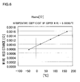
- Fig. 6 illustrates an example of a change in the resistance of copper wire with a change in temperature. If the element is used over a temperature range of 100°C, the resistance value of the wire varies by about 40% over this temperature range and this is accompanied by an approximately 40% change in the detected value of overcurrent.
- Patent Document 1 states as follows: "If it is so designed that a reference voltage circuit is afforded a temperature coefficient taking into consideration the temperature coefficient of the resistance of a bonding wire (wiring), then it will be possible to compensate for the temperature characteristic of the detected current value of overcurrent.” However, nowhere is a concrete method of compensating for the temperature characteristic described. It is therefore difficult to design a highly precise temperature compensating circuit using a simple circuit arrangement in a vehicle-mounted current detecting circuit.
- the inventor has discovered that a temperature coefficient at a potential difference across two diode groups through which constant currents are passed is the same as the temperature coefficient of electrical resistivity of a metal. Accordingly, the inventor has accomplished the present invention based on the idea that overcurrent detection having an outstanding temperature characteristic can be achieved by so arranging it that a current-limit value of overcurrent that flows into a metal wire is corrected based upon a potential difference across two groups of diodes.
- an overcurrent detecting circuit comprises: an output terminal; an output transistor for passing an output current into a load via the output terminal; a metal wire connected to the transistor and through which the output current flows; and a control circuit for detecting a potential difference.
- the potential difference is produced across both ends of the metal wire owing to the output current that flows into the metal wire and the resistance of the metal wire.
- the control circuit controls the transistor so as to limit the output current if the potential difference exceeds a prescribed value.
- the control circuit includes: first and second current sources; a first diode group having a first end from which a first current is passed in a forward direction by the first current source and a second end connected to a first end of the metal wire; and a second diode group having a first end from which a second current is passed in a forward direction by the second current source and a second end connected to a second end of the metal wire.
- the prescribed value is corrected based upon a potential difference across the first end of the first diode group and the first end of the second diode group so as to reduce a change in output-current limit value ascribable to a change in resistance of the wire with temperature.
- a semiconductor device that includes the overcurrent detecting circuit.
- the first diode group may have a first diode set having X-number of diode(s), where X is an integer equal to or greater than 1, of parallel-connected diodes constituting one first set in which anodes are connected in common and cathodes are connected in common, with L-number of the first diode set(s), where L is an integer equal to or greater than 1, of the first diode sets being connected serially in a forward direction.
- a cathode end (a second end) of the first diode group is connected to the first end of the metal wire.
- the second diode group may have a second diode set having Y-number of diode(s), where Y is an integer equal to or greater than 1, of parallel connected diodes constituting one second set in which anodes are connected in parallel and cathodes are connected in parallel, with L-number of the second diode set(s), where L is equal to that of the first diode group, of the second diode sets being connected serially in a forward direction.
- a cathode end (a second end) of the second diode group is connected to the second end of the metal wire.
- each diode of the first diode set and the second diode set has typically the same structural geometry.
- M ⁇ Y/N/X > 1 become M/N > 1, and the values of M and N can be selected so as to satisfy this formula.
- the control circuit may include: a first MOS transistor having a source, which is connected to an anode end (a first end) of the first diode group, and a drain and gate connected to the first current source; a second MOS transistor having a source connected to an anode end (a first end) of the second diode group, a drain connected to the second current source and a gate connected to the gate of the first MOS transistor; and a third MOS transistor having a gate connected to the drain of the second MOS transistor, a source connected to one of the first and second end of the metal wire and a drain connected to a control end of the output transistor.
- the first, second and third MOS transistors can be of the same conductivity type, and the third MOS transistor controls the output transistor so as to limit the output current if the potential difference exceeds the prescribed value.
- the output transistor may be an NMOS transistor that functions as one of a high-side switch and a low-side switch.
- a semiconductor device may include the overcurrent detecting circuit aforementioned.
- the first and second diode groups are placed close to the metal wire.
- the metal wire may be a bonding wire consisting of copper, silver, gold, aluminum or an alloy having at least one of these metals as a main component.
- the output terminal may be an outer lead portion of a lead frame to which the bonding wire is connected.
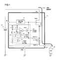
- An overcurrent detecting circuit includes: an output terminal OUT ( Fig. 1 ); an output transistor NM0 ( Fig. 1 ) for passing an output current Ia ( Fig. 1 ) into a load 12 ( Fig. 1 ) via the output terminal; a metal wire 17 ( Fig. 1 ) connected to the output transistor and through which the output current flows; and a control circuit 20 ( Fig. 1 ) for detecting a potential difference, which is produced across both ends of the metal wire owing to the output current that flows into the metal wire and the resistance of the metal wire, and controlling the output transistor so as to limit the output current if the potential difference exceeds a prescribed value.
- the control circuit 20 ( Fig. 1 ).
- first and second current sources 11 and 12 includes first and second current sources 11 and 12 ( Fig. 1 ); a first diode group 21 ( Fig. 1 ) having first ends from which a first current is passed in a forward direction by the first current source and second ends connected to a first end of the metal wire; and a second diode group 22 ( Fig. 1 ) having first ends from which a second current is passed in a forward direction by the second current source and second ends connected to a second end of the metal wire.
- the prescribed value is corrected based upon a potential difference across the first ends of the first and second diode groups so as to reduce a change in output-current limit value ascribable to a change in resistance of the metal wire with temperature.
- the first diode group has X-number (where X is an integer equal to or greater than 1) of parallel-connected diodes constituting one set in which anodes are connected in common and cathodes are connected in common, L-number (where L is an integer equal to or greater than 1) of the diode sets being connected serially in the forward direction and cathode ends of the diodes being connected to the first end of the metal wire.
- the second diode group has Y-number (where Y is an integer equal to or greater than 1) of diodes constituting one set in which anodes are connected in parallel and cathodes are connected in parallel, L-number of the diode sets being connected serially in the forward direction and cathode ends of the diodes being connected to the second end of the metal wire. It is so arranged that M ⁇ Y/N/X > 1 holds, where the potential at the second end of the metal wire is higher than the potential at the first end of the metal wire, and the current-value ratio of the first current source to the second current source is M:N (where M and N are positive integers).
- the control circuit includes: a first MOS transistor NM1 ( Fig. 4 ) having a source, which is connected to the anode ends of the first diode group, and a drain and gate connected to the first current source; a second MOS transistor NM2 ( Fig. 4 ) having a source connected to anode ends of the second diode group, a drain connected to the second current source and a gate connected to the gate of the first MOS transistor; and a third MOS transistor NM3 ( Fig. 4 ) having a gate connected to the drain of the second MOS transistor, a source connected to the first or second end of the metal wire and a drain connected to a control end of the output transistor NM0 ( Fig. 4 ).
- the first, second and third MOS transistors are of the same conductivity type, and the third MOS transistor controls the output transistor so as to limit the output current if the potential difference exceeds the prescribed value.
- the output transistor may be an NMOS transistor that functions as a high-side switch or low-side switch.
- a semiconductor device includes the overcurrent detecting circuit described above. It is preferred that the first and second diode groups be placed close to the metal wire in the semiconductor device. Further, the metal wire may be a bonding wire consisting of copper, silver, gold, aluminum or an alloy having at least one of these metals as a main component.
- the output terminal may be a lead frame to which the bonding wire is connected.
- Fig. 1 is a circuit diagram illustrating a semiconductor device 10 according to a first exemplary embodiment of the present invention.
- the semiconductor device 10 has terminals Vcc, IN, GND and OUT, an NMOS transistor NM0, a boosting circuit 15, a wire 17 and a control circuit 20.
- the boosting circuit 15 impresses a boosted voltage upon the gate of the NMOS transistor NM0.
- the NMOS transistor NM0 to the gate of which the boosted voltage has been applied turns on so that a load current (output current) Ia supplied from a battery 11 is output from the terminal OUT and supplied to a load 12 via the terminal Vcc, drain and source of the NMOS transistor NM0 and wire 17.
- the control circuit 20 has diode groups 21, 22, current sources I1, I2, an amplifier AMP and an NMOS transistor NM3.
- the diode group 21 has first ends (the anode side) from which a first current is passed in a forward direction by the current source 11 and second ends (the cathode side) connected to a first end (point B) of the wire 17.
- the diode group 22 has first ends (the anode side) from which a first current is passed in a forward direction by the current source I2 and second ends (the cathode side) connected to a second end (point A) of the wire 17. It is assumed that the current values in the current sources 11, 12 are so small as to be negligible in comparison with the current value of the load current Ia.
- the amplifier AMP has an inverting input terminal (-) connected to the first ends (anode side) of the diode group 21, a non-inverting input terminal (+) connected to the first ends (anode side) of the diode group 22, and an output terminal connected to the gate of the NMOS transistor NM3.
- the NMOS transistor NM3 has a drain connected to the gate of the NMOS transistor NM0 and a source connected to the second end (point A) of the wire 17, namely to the source of the NMOS transistor NM0.
- the potential difference across the ends (points A and B) of the wire 17 is small and the potential at the first ends (anode side) of the diode group 22, namely the potential at the non-inverting input terminal of the amplifier AMP, is lower than the potential at the first ends (anode side) of the diode group 21, namely the potential at the inverting input terminal of the amplifier AMP. Accordingly, the potential at the output of the amplifier AMP declines, the NMOS transistor NM3 turns off and operation of the NMOS transistor NM0 is unaffected.
- the control circuit 20 controls the gate of the NMOS transistor NM0 so as to limit the load current Ia. More specifically, if the potential at the first ends (anode side) of the diode group 22 becomes higher than the potential at the first ends (anode side) of the diode group 21, then the potential at the output terminal of the amplifier AMP rises.
- the potential difference across the gate and source of the NMOS transistor NM3 increases, the potential at the drain of the NMOS transistor NM3, namely the potential at the gate of the NMOS transistor NM0, falls and the load current Ia that flows through the NMOS transistor NM0 is limited.
- the diode group 21 has X-number (where X is an integer equal to or greater than 1) of parallel-connected diodes constituting one set in which the anodes are connected in common and the cathodes are connected in common, L-number (where L is an integer equal to or greater than 1) of these diode sets being connected serially in the forward direction.
- the diode group 22 has Y-number (where Y is an integer equal to or greater than 1) of parallel-connected diodes constituting one set in which the anodes are connected in common and the cathodes are connected in common, L-number of these diode sets being connected serially in the forward direction.
- the current-value ratio of the first current source I1 to the second current source I2 is M:N (where M and N are positive integers).
- the resistance value of the wire 17 is R.
- Ia L ⁇ k / q ⁇ ( T + 273 ) ⁇ ln M ⁇ Y / N / X / R / 1 + tc ⁇ T - 25
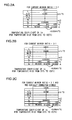
- Figs. 2A to 2C illustrate examples of cases where the metal constituting the wire 17 is copper, the resistance value of the wire 17 is 1 m ⁇ and temperature is varied to values of -40°C, 25°C and 125°C.
- the temperature coefficient of the output-current limit value of the load current Ia when temperature is varied from 25°C to 125°C is -0.00041/°C. That is, these results indicate that in a case where temperature is varied by 100°C, the variation in output-current limit value falls within 4%.
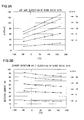
- Fig. 3A is a graph illustrating a change in potential difference ⁇ VF across the diode groups 21, 22 when temperature is varied.
- Fig. 3B is a graph illustrating a change in detected current (output-current limit value) when temperature is varied.
- the temperature coefficient of the potential difference across the diode groups 21 and 22 becomes a value close to the temperature coefficient of the copper wire shown in Fig. 6 , and that the change in the output-current limit value (detected value) with temperature is kept small, as illustrated in Fig. 3B .
- the example illustrated is one in which the load 12 is connected between the terminal OUT and ground and the NMOS transistor NM0 functions as a high-side switch.
- the terminal OUT is grounded, the load 12 is connected between the terminal Vcc and the battery 11 and the NMOS transistor NM0 functions as a low-side switch.
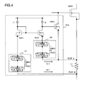
- Fig. 4 is a circuit diagram of an overcurrent detecting circuit according to a second exemplary embodiment of the present invention. Components in Fig. 4 identical with those shown in Fig. 1 are designated by like reference characters and need not be described again.
- the overcurrent detecting circuit shown in Fig. 4 is obtained by incorporating a current mirror, which comprises NMOS transistors NM1, NM2, in a control circuit 20a in place of the amplifier AMP of Fig. 1 .
- the MOS transistor NM1 has a source connected to the anode side of the diode group 21, and a drain and gate connected to the current source 11.
- the MOS transistor MN2 has a source connected to the anode side of the diode group 21, a drain connected to the current source I2 and a gate connected to the gate of the MOS transistor NM1.
- the NMOS transistor NM3 has its gate connected to the drain of the MOS transistor NM2, its source connected to the second end (point A) of the wire 17 and its drain connected to the gate (control end) of the NMOS transistor NM0. It should be noted that the arrangement is such that the size ratio between the NMOS transistors MN1 and MN2 will agree with the current ratio between the current sources 11 and 12.
- the potential difference across the ends (points A and B) of the wire 17 is small and the potential at the first ends (anode side) of the diode group 22, namely the potential at the source of the NMOS transistor NM2, is lower than the potential at the first ends (anode side) of the diode group 21, namely the potential at the source of the NMOS transistor NM1. Accordingly, the NMOS transistor NM2 turns on and the potential at the gate of the NMOS transistor NM3 declines. Consequently, the NMOS transistor NM3 turns off and operation of the NMOS transistor NM0 is unaffected. It should be noted that the size of the NMOS transistor NM3 is set in such a manner that the NMOS transistor NM3 will not be turned on by the turned-on NMOS transistor NM2 and voltage drop of the diode group 22.
- the load current Ia exceeds an output-current limit value
- the potential difference across the ends (points A and B) of the wire 17 will exceed a prescribed value.
- the first end (anode side) of the diode group 22 becomes higher than the potential at the first end (anode side) of the diode group 21 and the NMOS transistor NM2 turns off. Accordingly, the potential at the gate of the NMOS transistor NM3 rises owing to current that flows out of the current source I2.
- the potential difference across the gate and source of the NMOS transistor NM3 increases, the potential at the drain of the NMOS transistor NM3, namely the potential at the gate of the NMOS transistor NM0, falls and the load current Ia that flows through the NMOS transistor NM0 is limited.
- overcurrent can be detected by a simply constructed circuit and a change in the output-current limit value (detected current) with temperature is kept low.
- Fig. 5 is a diagram illustrating the structure of a semiconductor device according to a third exemplary embodiment of the present invention. Components in Fig. 5 identical with those shown in Fig. 1 are designated by like reference characters.
- the semiconductor device illustrated in Fig. 5 has an IPD chip 30, terminals Vcc, In, GND and OUT, and wires 17, 18a, 18b, 19.
- the IPD chip 30, which is placed on a lead frame to which the terminal Vcc is connected, has the NMOS transistor NM0, boosting circuit 15 and control circuit 20, etc.
- the placed components such as the boosting circuit 15 and control circuit 20 are connected to the terminals IN and GND by the wires (bonding wires) 18a and 18b, respectively, they are wired to the NMOS transistor NM0 by a surface metal (which corresponds to point A) and are connected to the lead frame, which is the terminal OUT, by the wire (bonding wire) 19. Further, the NMOS transistor NM0 has its drain connected to the terminal Vcc (the lead frame on which the IPD chip 30 is mounted), its source connected by the wire 17 to the lead frame serving as the terminal OUT, and its drain wired to the control circuit 20 by wiring (not shown).
- Vcc the lead frame on which the IPD chip 30 is mounted
- the wire 17 be a bonding wire consisting of a metal such as copper, silver, gold or aluminum or an alloy having at least one of these metals as a main component. Further, it is preferred that the diode groups 21, 22 in the control circuit 20 be placed close to the wire 17 so as to diminish the temperature difference between diode groups 21, 22 and the wire 17, although this is not illustrated.
- the temperature difference between the diode groups 21, 22 and the wire 17 is small and the temperature coefficient at the potential difference across the two diode groups is the same as the temperature coefficient of the electrical resistivity of the wire 17.
- the detected voltage of the output-current limit value is corrected so as to reduce the change in output-current limit value.
- a variation in the resistance value R of the bonding wire 17 is ascribable to a variation in material, diameter and length of the wire.
- An example of such variation is roughly ⁇ 5% at 3 ⁇ (where ⁇ represents a standard deviation).
- the potential difference ⁇ VF across the diode groups is a relative value and exhibits a small variation.
- An example of such variation is roughly ⁇ 3 % at 3 ⁇ . That is, the precision of the resistance value and the precision of the reference voltage value are high and the precision of current detection is excellent.
- the temperature coefficient of the potential difference ⁇ VF is 0.00336 (/°C) irrespective of X and Y illustrated earlier, and the graph of the temperature characteristic is as depicted in Fig. 3A illustrated earlier.
- the temperature coefficient (rate of increase per 1°C) of the resistance value R of the bonding wire is decided by the wire material.
- the temperature coefficient in the case of a copper (Cu) wire is 0.00393 (/°C)
- the graph of the temperature characteristic is as depicted in Fig. 6 illustrated earlier.
- the resistance temperature coefficients of silver, gold and aluminum are 0.0038 (/°C), 0.0034 (/°C) and 0.0039 (/°C), respectively. These are approximately the same as the resistance temperature coefficient of copper and are close to the temperature coefficient of the potential difference ⁇ VF.
- the semiconductor device described above is ideal for use as a vehicle-mounted high-side switch and furnishes a highly precise temperature compensation in an overcurrent detecting circuit.
Landscapes
- Electronic Switches (AREA)
- Amplifiers (AREA)
- Power Conversion In General (AREA)
Applications Claiming Priority (1)
| Application Number | Priority Date | Filing Date | Title |
|---|---|---|---|
| JP2007074943A JP4919847B2 (ja) | 2007-03-22 | 2007-03-22 | 過電流検出回路および半導体装置 |
Publications (2)
| Publication Number | Publication Date |
|---|---|
| EP1973229A1 true EP1973229A1 (de) | 2008-09-24 |
| EP1973229B1 EP1973229B1 (de) | 2010-06-09 |
Family
ID=39523517
Family Applications (1)
| Application Number | Title | Priority Date | Filing Date |
|---|---|---|---|
| EP08005171A Expired - Fee Related EP1973229B1 (de) | 2007-03-22 | 2008-03-19 | Überstromerkennungsschaltung und Halbleitervorrichtung |
Country Status (4)
| Country | Link |
|---|---|
| US (1) | US7660091B2 (de) |
| EP (1) | EP1973229B1 (de) |
| JP (1) | JP4919847B2 (de) |
| DE (1) | DE602008001453D1 (de) |
Families Citing this family (9)
| Publication number | Priority date | Publication date | Assignee | Title |
|---|---|---|---|---|
| JP4929020B2 (ja) * | 2007-04-10 | 2012-05-09 | 矢崎総業株式会社 | 負荷回路の過電流保護装置 |
| CN102035165B (zh) * | 2009-09-29 | 2014-07-30 | 意法半导体研发(上海)有限公司 | 用于短路保护的系统和方法 |
| JP5431994B2 (ja) * | 2010-02-10 | 2014-03-05 | ルネサスエレクトロニクス株式会社 | 電流制限回路 |
| JP2011200035A (ja) * | 2010-03-19 | 2011-10-06 | Aisin Seiki Co Ltd | 車両用過電流検出装置 |
| JP5581907B2 (ja) | 2010-09-01 | 2014-09-03 | 株式会社リコー | 半導体集積回路及び半導体集積回路装置 |
| JP5637105B2 (ja) * | 2011-09-19 | 2014-12-10 | 株式会社デンソー | 過電流保護回路 |
| US10193326B2 (en) * | 2016-04-21 | 2019-01-29 | Continental Automotive Systems, Inc. | Non-intrusive short-circuit protection for power supply devices |
| JP2023184189A (ja) * | 2022-06-17 | 2023-12-28 | ローム株式会社 | 半導体チップ、半導体装置 |
| EP4391380A1 (de) * | 2022-12-20 | 2024-06-26 | Infineon Technologies Austria AG | Co-verpackte kontrollierte überstromhandhabung |
Citations (10)
| Publication number | Priority date | Publication date | Assignee | Title |
|---|---|---|---|---|
| EP0402928A2 (de) | 1989-06-16 | 1990-12-19 | National Semiconductor Corporation | Schaltung zur internen Strombegrenzung für schnellen Leistungsschalter |
| JPH0348737A (ja) * | 1989-07-17 | 1991-03-01 | Nec Corp | 温度検出回路 |
| JPH06216307A (ja) | 1993-01-13 | 1994-08-05 | Mitsubishi Electric Corp | 樹脂封止型半導体装置 |
| DE4429716C1 (de) | 1994-08-22 | 1996-02-01 | Siemens Ag | Schaltungsanordnung zur Strombegrenzung |
| US5519341A (en) | 1994-12-02 | 1996-05-21 | Texas Instruments Incorporated | Cross coupled quad comparator for current sensing independent of temperature |
| WO1996018109A2 (en) * | 1994-12-09 | 1996-06-13 | National Semiconductor Corporation | An integrated resistor for sensing electrical parameters |
| JPH11121683A (ja) | 1997-10-08 | 1999-04-30 | Nissan Motor Co Ltd | 半導体集積回路 |
| JP2000213992A (ja) | 1999-01-26 | 2000-08-04 | Nissan Motor Co Ltd | 温度検出回路及び半導体装置 |
| JP2001267899A (ja) * | 2000-03-16 | 2001-09-28 | Denso Corp | 負荷駆動回路 |
| JP2004080087A (ja) | 2002-08-09 | 2004-03-11 | Renesas Technology Corp | 過電流検出回路 |
Family Cites Families (11)
| Publication number | Priority date | Publication date | Assignee | Title |
|---|---|---|---|---|
| US4945445A (en) * | 1988-09-29 | 1990-07-31 | Gentron Corporation | Current sense circuit |
| JPH0666600B2 (ja) * | 1989-10-02 | 1994-08-24 | 株式会社東芝 | 電流検出回路 |
| JP3427436B2 (ja) * | 1993-09-16 | 2003-07-14 | 株式会社デンソー | 駆動回路 |
| JP3753492B2 (ja) * | 1997-01-29 | 2006-03-08 | ローム株式会社 | 電源監視ic及び電池パック |
| DE19742930C1 (de) * | 1997-09-29 | 1998-11-19 | Siemens Ag | Leistungsschalter mit Überlastschutz |
| JP3656412B2 (ja) * | 1998-07-03 | 2005-06-08 | 株式会社日立製作所 | 車両用電力制御装置 |
| US6351360B1 (en) * | 1999-09-20 | 2002-02-26 | National Semiconductor Corporation | Apparatus for selective shutdown of devices of an integrated circuit in response to thermal fault detection |
| JP3688619B2 (ja) * | 2001-10-05 | 2005-08-31 | 株式会社東芝 | 半導体集積回路 |
| US6867573B1 (en) * | 2003-11-07 | 2005-03-15 | National Semiconductor Corporation | Temperature calibrated over-current protection circuit for linear voltage regulators |
| US7499253B2 (en) * | 2005-03-07 | 2009-03-03 | Rohm Co., Ltd. | Semiconductor integrated-circuit unit with temperature protective circuit |
| JP2008198821A (ja) * | 2007-02-14 | 2008-08-28 | Ricoh Co Ltd | 過熱保護回路を備える定電圧回路を内蔵した半導体装置 |
-
2007
- 2007-03-22 JP JP2007074943A patent/JP4919847B2/ja not_active Expired - Fee Related
-
2008
- 2008-03-18 US US12/076,404 patent/US7660091B2/en not_active Expired - Fee Related
- 2008-03-19 DE DE602008001453T patent/DE602008001453D1/de active Active
- 2008-03-19 EP EP08005171A patent/EP1973229B1/de not_active Expired - Fee Related
Patent Citations (10)
| Publication number | Priority date | Publication date | Assignee | Title |
|---|---|---|---|---|
| EP0402928A2 (de) | 1989-06-16 | 1990-12-19 | National Semiconductor Corporation | Schaltung zur internen Strombegrenzung für schnellen Leistungsschalter |
| JPH0348737A (ja) * | 1989-07-17 | 1991-03-01 | Nec Corp | 温度検出回路 |
| JPH06216307A (ja) | 1993-01-13 | 1994-08-05 | Mitsubishi Electric Corp | 樹脂封止型半導体装置 |
| DE4429716C1 (de) | 1994-08-22 | 1996-02-01 | Siemens Ag | Schaltungsanordnung zur Strombegrenzung |
| US5519341A (en) | 1994-12-02 | 1996-05-21 | Texas Instruments Incorporated | Cross coupled quad comparator for current sensing independent of temperature |
| WO1996018109A2 (en) * | 1994-12-09 | 1996-06-13 | National Semiconductor Corporation | An integrated resistor for sensing electrical parameters |
| JPH11121683A (ja) | 1997-10-08 | 1999-04-30 | Nissan Motor Co Ltd | 半導体集積回路 |
| JP2000213992A (ja) | 1999-01-26 | 2000-08-04 | Nissan Motor Co Ltd | 温度検出回路及び半導体装置 |
| JP2001267899A (ja) * | 2000-03-16 | 2001-09-28 | Denso Corp | 負荷駆動回路 |
| JP2004080087A (ja) | 2002-08-09 | 2004-03-11 | Renesas Technology Corp | 過電流検出回路 |
Also Published As
| Publication number | Publication date |
|---|---|
| US20080232017A1 (en) | 2008-09-25 |
| JP2008236528A (ja) | 2008-10-02 |
| JP4919847B2 (ja) | 2012-04-18 |
| US7660091B2 (en) | 2010-02-09 |
| DE602008001453D1 (de) | 2010-07-22 |
| EP1973229B1 (de) | 2010-06-09 |
Similar Documents
| Publication | Publication Date | Title |
|---|---|---|
| EP1973229B1 (de) | Überstromerkennungsschaltung und Halbleitervorrichtung | |
| US8467165B2 (en) | Power supply control apparatus including overcurrent detection circuit | |
| EP2355354B1 (de) | Strombegrenzungsschaltung | |
| US8093889B2 (en) | Sensor circuit | |
| CN110095647A (zh) | 半导体器件、负载驱动系统和电感器电流的电流感测的方法 | |
| JP5168413B2 (ja) | 電圧駆動型素子を駆動する駆動装置 | |
| KR101240910B1 (ko) | 정전압 전원 회로 | |
| JP5767847B2 (ja) | 基準電流生成回路及びこれを用いた電源装置 | |
| WO2006016456A1 (ja) | 回路の保護方法、保護回路およびそれを利用した電源装置 | |
| CN116707501B (zh) | 智能电子开关、集成电路芯片、芯片产品和汽车 | |
| CN102243262A (zh) | 电流检测电路 | |
| WO2014199816A1 (ja) | 過電流検出回路 | |
| US7109761B2 (en) | Comparator circuit | |
| US20060066286A1 (en) | Overcurrent detection method and detection circuit | |
| US20110291741A1 (en) | Current Control Using Thermally Matched Resistors | |
| US5656968A (en) | Circuit arrangement for regulating the load current of a power MOSFET | |
| US20100207605A1 (en) | Power supply control apparatus including overcurrent detection circuit | |
| US11899043B2 (en) | Current detection apparatus and power supply control apparatus | |
| US20100117611A1 (en) | Regulator circuit having N-type MOS transistor controlled by error amplifier | |
| CN112305291A (zh) | 电压监视电路 | |
| JP3311498B2 (ja) | 半導体装置 | |
| JP7611531B2 (ja) | 判定装置及びそれを備えるスイッチシステム | |
| CN221631889U (zh) | 电压调节电路、高压调节电路以及设备 | |
| US20070290761A1 (en) | Signal amplifier circuit | |
| JP5848516B2 (ja) | 電源装置 |
Legal Events
| Date | Code | Title | Description |
|---|---|---|---|
| PUAI | Public reference made under article 153(3) epc to a published international application that has entered the european phase |
Free format text: ORIGINAL CODE: 0009012 |
|
| AK | Designated contracting states |
Kind code of ref document: A1 Designated state(s): AT BE BG CH CY CZ DE DK EE ES FI FR GB GR HR HU IE IS IT LI LT LU LV MC MT NL NO PL PT RO SE SI SK TR |
|
| AX | Request for extension of the european patent |
Extension state: AL BA MK RS |
|
| 17P | Request for examination filed |
Effective date: 20090318 |
|
| AKX | Designation fees paid |
Designated state(s): DE |
|
| 17Q | First examination report despatched |
Effective date: 20090923 |
|
| GRAP | Despatch of communication of intention to grant a patent |
Free format text: ORIGINAL CODE: EPIDOSNIGR1 |
|
| GRAS | Grant fee paid |
Free format text: ORIGINAL CODE: EPIDOSNIGR3 |
|
| GRAA | (expected) grant |
Free format text: ORIGINAL CODE: 0009210 |
|
| AK | Designated contracting states |
Kind code of ref document: B1 Designated state(s): DE |
|
| REF | Corresponds to: |
Ref document number: 602008001453 Country of ref document: DE Date of ref document: 20100722 Kind code of ref document: P |
|
| RAP2 | Party data changed (patent owner data changed or rights of a patent transferred) |
Owner name: RENESAS ELECTRONICS CORPORATION |
|
| PLBE | No opposition filed within time limit |
Free format text: ORIGINAL CODE: 0009261 |
|
| STAA | Information on the status of an ep patent application or granted ep patent |
Free format text: STATUS: NO OPPOSITION FILED WITHIN TIME LIMIT |
|
| REG | Reference to a national code |
Ref country code: DE Ref legal event code: R097 Ref document number: 602008001453 Country of ref document: DE Effective date: 20110309 |
|
| REG | Reference to a national code |
Ref country code: DE Ref legal event code: R082 Ref document number: 602008001453 Country of ref document: DE Representative=s name: GLAWE DELFS MOLL - PARTNERSCHAFT VON PATENT- U, DE |
|
| REG | Reference to a national code |
Ref country code: DE Ref legal event code: R081 Ref document number: 602008001453 Country of ref document: DE Owner name: RENESAS ELECTRONICS CORPORATION, JP Free format text: FORMER OWNER: NEC ELECTRONICS CORP., KAWASAKI, JP Effective date: 20120828 Ref country code: DE Ref legal event code: R082 Ref document number: 602008001453 Country of ref document: DE Representative=s name: GLAWE DELFS MOLL - PARTNERSCHAFT VON PATENT- U, DE Effective date: 20120828 Ref country code: DE Ref legal event code: R081 Ref document number: 602008001453 Country of ref document: DE Owner name: RENESAS ELECTRONICS CORPORATION, KAWASAKI-SHI, JP Free format text: FORMER OWNER: NEC ELECTRONICS CORP., KAWASAKI, KANAGAWA, JP Effective date: 20120828 Ref country code: DE Ref legal event code: R082 Ref document number: 602008001453 Country of ref document: DE Representative=s name: GLAWE DELFS MOLL PARTNERSCHAFT MBB VON PATENT-, DE Effective date: 20120828 |
|
| PGFP | Annual fee paid to national office [announced via postgrant information from national office to epo] |
Ref country code: DE Payment date: 20130314 Year of fee payment: 6 |
|
| REG | Reference to a national code |
Ref country code: DE Ref legal event code: R119 Ref document number: 602008001453 Country of ref document: DE |
|
| REG | Reference to a national code |
Ref country code: DE Ref legal event code: R119 Ref document number: 602008001453 Country of ref document: DE Effective date: 20141001 |
|
| PG25 | Lapsed in a contracting state [announced via postgrant information from national office to epo] |
Ref country code: DE Free format text: LAPSE BECAUSE OF NON-PAYMENT OF DUE FEES Effective date: 20141001 |