EP1978127A1 - Dispositif de projection et procede de formation de film - Google Patents
Dispositif de projection et procede de formation de film Download PDFInfo
- Publication number
- EP1978127A1 EP1978127A1 EP07706806A EP07706806A EP1978127A1 EP 1978127 A1 EP1978127 A1 EP 1978127A1 EP 07706806 A EP07706806 A EP 07706806A EP 07706806 A EP07706806 A EP 07706806A EP 1978127 A1 EP1978127 A1 EP 1978127A1
- Authority
- EP
- European Patent Office
- Prior art keywords
- targets
- sputtering
- film
- voltage
- sputtering apparatus
- Prior art date
- Legal status (The legal status is an assumption and is not a legal conclusion. Google has not performed a legal analysis and makes no representation as to the accuracy of the status listed.)
- Withdrawn
Links
Images



Classifications
-
- C—CHEMISTRY; METALLURGY
- C23—COATING METALLIC MATERIAL; COATING MATERIAL WITH METALLIC MATERIAL; CHEMICAL SURFACE TREATMENT; DIFFUSION TREATMENT OF METALLIC MATERIAL; COATING BY VACUUM EVAPORATION, BY SPUTTERING, BY ION IMPLANTATION OR BY CHEMICAL VAPOUR DEPOSITION, IN GENERAL; INHIBITING CORROSION OF METALLIC MATERIAL OR INCRUSTATION IN GENERAL
- C23C—COATING METALLIC MATERIAL; COATING MATERIAL WITH METALLIC MATERIAL; SURFACE TREATMENT OF METALLIC MATERIAL BY DIFFUSION INTO THE SURFACE, BY CHEMICAL CONVERSION OR SUBSTITUTION; COATING BY VACUUM EVAPORATION, BY SPUTTERING, BY ION IMPLANTATION OR BY CHEMICAL VAPOUR DEPOSITION, IN GENERAL
- C23C14/00—Coating by vacuum evaporation, by sputtering or by ion implantation of the coating forming material
- C23C14/22—Coating by vacuum evaporation, by sputtering or by ion implantation of the coating forming material characterised by the process of coating
- C23C14/34—Sputtering
- C23C14/3407—Cathode assembly for sputtering apparatus, e.g. Target
-
- C—CHEMISTRY; METALLURGY
- C23—COATING METALLIC MATERIAL; COATING MATERIAL WITH METALLIC MATERIAL; CHEMICAL SURFACE TREATMENT; DIFFUSION TREATMENT OF METALLIC MATERIAL; COATING BY VACUUM EVAPORATION, BY SPUTTERING, BY ION IMPLANTATION OR BY CHEMICAL VAPOUR DEPOSITION, IN GENERAL; INHIBITING CORROSION OF METALLIC MATERIAL OR INCRUSTATION IN GENERAL
- C23C—COATING METALLIC MATERIAL; COATING MATERIAL WITH METALLIC MATERIAL; SURFACE TREATMENT OF METALLIC MATERIAL BY DIFFUSION INTO THE SURFACE, BY CHEMICAL CONVERSION OR SUBSTITUTION; COATING BY VACUUM EVAPORATION, BY SPUTTERING, BY ION IMPLANTATION OR BY CHEMICAL VAPOUR DEPOSITION, IN GENERAL
- C23C14/00—Coating by vacuum evaporation, by sputtering or by ion implantation of the coating forming material
- C23C14/22—Coating by vacuum evaporation, by sputtering or by ion implantation of the coating forming material characterised by the process of coating
- C23C14/34—Sputtering
- C23C14/35—Sputtering by application of a magnetic field, e.g. magnetron sputtering
- C23C14/352—Sputtering by application of a magnetic field, e.g. magnetron sputtering using more than one target
-
- C—CHEMISTRY; METALLURGY
- C23—COATING METALLIC MATERIAL; COATING MATERIAL WITH METALLIC MATERIAL; CHEMICAL SURFACE TREATMENT; DIFFUSION TREATMENT OF METALLIC MATERIAL; COATING BY VACUUM EVAPORATION, BY SPUTTERING, BY ION IMPLANTATION OR BY CHEMICAL VAPOUR DEPOSITION, IN GENERAL; INHIBITING CORROSION OF METALLIC MATERIAL OR INCRUSTATION IN GENERAL
- C23C—COATING METALLIC MATERIAL; COATING MATERIAL WITH METALLIC MATERIAL; SURFACE TREATMENT OF METALLIC MATERIAL BY DIFFUSION INTO THE SURFACE, BY CHEMICAL CONVERSION OR SUBSTITUTION; COATING BY VACUUM EVAPORATION, BY SPUTTERING, BY ION IMPLANTATION OR BY CHEMICAL VAPOUR DEPOSITION, IN GENERAL
- C23C14/00—Coating by vacuum evaporation, by sputtering or by ion implantation of the coating forming material
- C23C14/06—Coating by vacuum evaporation, by sputtering or by ion implantation of the coating forming material characterised by the coating material
- C23C14/10—Glass or silica
-
- G—PHYSICS
- G11—INFORMATION STORAGE
- G11B—INFORMATION STORAGE BASED ON RELATIVE MOVEMENT BETWEEN RECORD CARRIER AND TRANSDUCER
- G11B5/00—Recording by magnetisation or demagnetisation of a record carrier; Reproducing by magnetic means; Record carriers therefor
- G11B5/84—Processes or apparatus specially adapted for manufacturing record carriers
- G11B5/85—Coating a support with a magnetic layer by vapour deposition
-
- H—ELECTRICITY
- H01—ELECTRIC ELEMENTS
- H01J—ELECTRIC DISCHARGE TUBES OR DISCHARGE LAMPS
- H01J37/00—Discharge tubes with provision for introducing objects or material to be exposed to the discharge, e.g. for the purpose of examination or processing thereof
- H01J37/32—Gas-filled discharge tubes
- H01J37/34—Gas-filled discharge tubes operating with cathodic sputtering
-
- H—ELECTRICITY
- H01—ELECTRIC ELEMENTS
- H01J—ELECTRIC DISCHARGE TUBES OR DISCHARGE LAMPS
- H01J37/00—Discharge tubes with provision for introducing objects or material to be exposed to the discharge, e.g. for the purpose of examination or processing thereof
- H01J37/32—Gas-filled discharge tubes
- H01J37/34—Gas-filled discharge tubes operating with cathodic sputtering
- H01J37/3402—Gas-filled discharge tubes operating with cathodic sputtering using supplementary magnetic fields
- H01J37/3405—Magnetron sputtering
-
- H—ELECTRICITY
- H01—ELECTRIC ELEMENTS
- H01J—ELECTRIC DISCHARGE TUBES OR DISCHARGE LAMPS
- H01J37/00—Discharge tubes with provision for introducing objects or material to be exposed to the discharge, e.g. for the purpose of examination or processing thereof
- H01J37/32—Gas-filled discharge tubes
- H01J37/34—Gas-filled discharge tubes operating with cathodic sputtering
- H01J37/3411—Constructional aspects of the reactor
- H01J37/3414—Targets
-
- H—ELECTRICITY
- H01—ELECTRIC ELEMENTS
- H01J—ELECTRIC DISCHARGE TUBES OR DISCHARGE LAMPS
- H01J37/00—Discharge tubes with provision for introducing objects or material to be exposed to the discharge, e.g. for the purpose of examination or processing thereof
- H01J37/32—Gas-filled discharge tubes
- H01J37/34—Gas-filled discharge tubes operating with cathodic sputtering
- H01J37/3411—Constructional aspects of the reactor
- H01J37/3414—Targets
- H01J37/3423—Shape
Definitions
- the present invention generally relates to a sputtering apparatus and a film forming method using the sputtering apparatus.
- a production method by means of reactive sputtering in which active gas is introduced to a sputtering space and sputtering materials obtained from a target react to the active gas and a compound film is deposited, has been known.
- a cathode In this reactive sputtering, a cathode is usually disposed in parallel with a substrate. Thus, sputtering particles that are discharged perpendicularly from a target on the cathode are incident on the substrate. Since such sputtering particles have high energy, there has been a problem in that, when a dielectric film is formed on the substrate, the dielectric film becomes damaged.
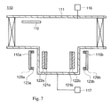
- Reference numeral 110 in FIG. 7 indicates a conventional facing target sputtering apparatus.
- the sputtering apparatus 110 is provided with a vacuum chamber 111, and in the vacuum chamber 111, two targets 121a and 121b are disposed such that their surfaces are in parallel and face each other with a certain space between them.
- the back faces of the targets 121a and 121b are mounted to cathode electrodes 122a and 122b, respectively.
- Magnetic members 115a and 115b are disposed on the back face of the cathode electrodes 122a and 122b.
- the magnetic members 115a and 115b are configured by installing ring-shaped magnets 123a and 123b to yokes 129a and 129b.
- the magnets 123a and 123b are respectively disposed that one of the magnetic poles thereof is directed toward the targets 121a and 121b and the other magnetic pole thereof is directed in the opposite direction, to the targets. Furthermore, the magnets 123a and 123b are disposed in such a manner that different polarity of magnetic poles of the magnets 123a and 123b are directed to the targets 121a and 121b.
- the south pole of the other magnet 123b is directed toward the target 121b. Since the magnets 123a and 123b are in a ring shape, magnetic lines of force are formed in a cylindrical shape between the magnets 123a and 123b.
- the inside of the vacuum chamber 111 is evacuated by vacuum evacuation system 116; sputtering gas is introduced from gas feeding system; and voltage is applied to the target 121a and 121b. Consequently, plasma of sputtering gas is generated in the space interposed between the targets 121a and 121b so that the surface of the targets 121a, 121b are sputtered.
- An object to be film formed 113 is disposed lateral to the space sandwiched between the targets 121a and 121b.
- a film is formed on the surface of the object to be film formed 113 by the sputtering particles that are obliquely sputtered from the targets 121a and 121b in order to discharge to the inside of the vacuum chamber 111.
- particles having high-speed energy can be confined between a pair of the targets using the magnetic lines of force in a cylindrical shape.
- inert gas is used as sputtering gas in conventional sputtering
- active gas is used in addition to inert gas as sputtering gas, and a film is formed with a reacted product of the solid particles that are sputtered from the targets and the active gas.
- the present invention is made in order to solve the above-mentioned problems, and it is an object thereof to provide a sputtering apparatus that does not cause abnormal discharges even when a dielectric film is formed.
- the present invention is a sputtering apparatus having first and second targets that are disposed such that their surfaces face each other, a third target disposed such that its surface is in parallel with the surface of the first target, a fourth target disposed such that its surface is in parallel with the surface of the second target and the fourth target faces the third target, and first to fourth cathode electrodes are disposed in the back of the first to fourth targets, wherein a film is formed on the surface of an object to be film formed at a location that faces a space between the first and the second targets.
- a sputtering apparatus is constructed such that the surfaces of the third and the fourth targets are located on the same plane where the surfaces of the first and the second targets are respectively positioned.
- a sputtering apparatus is constructed such that the first and the second targets are disposed between the object to be film formed on which the film is being formed and the third and the fourth targets.
- the sputtering apparatus includes a transfer mechanism for transferring the object to be film formed while the object to be film formed faces the space positioned between the first and the second targets.
- the sputtering apparatus is constructed such that the third and the fourth targets are disposed so that the object to be film formed on which the film is being formed faces a space between the third and the fourth targets.
- the sputtering apparatus is provided with a transfer mechanism for transferring the object to be film formed in such a manner that the object to be film formed simultaneously faces the space between the first and the second targets as well as the space between the third and the fourth targets.
- the sputtering apparatus includes a sputtering power source that is connected with the first to the fourth cathode electrodes and outputs an alternating current voltage, the sputtering power source is connected so as to apply a voltage of the same polarity and the same size to the first and the second cathode electrodes. Also, the sputtering power source is connected so as to apply a voltage having the same polarity and of the same size to the third and the fourth cathode electrodes.
- the sputtering apparatus is constructed such that the sputtering power source outputs an alternate current voltage in such a manner that, when a negative voltage is applied to the first and the second cathode electrodes, a voltage that is positive relative to the first and the second cathode electrodes is applied to the third and the fourth cathode electrodes; and in such a manner, when a negative voltage is applied to the third and the fourth cathode electrodes, a voltage that is positive relative to the third and the fourth cathode electrodes is applied to the first and the second cathode electrodes.
- the present invention is a method for forming a dielectric film using a sputtering apparatus, the sputtering apparatus including first and second targets disposed such that their surfaces face each other, a third target disposed such that its face is in parallel with the surface of the first target, and a fourth target disposed such that its surface is in parallel with the surface of the second target and faces the third target, the method for forming the dielectric film on an object to be film formed at a location facing a space positioned between the first and the second targets including, alternately repeating a first voltage period in which a negative voltage is applied to the first and the second targets and a voltage that is positive relative to the first and the second targets is applied to the third and the fourth targets, and a second voltage period in which a negative voltage is applied to the third and the fourth targets and a voltage that is positive relative to the third and the fourth targets is applied to the first and the second targets.
- a film forming method is constructed such that the dielectric film is formed by moving the object to be film formed while the object to be film formed faces a space positioned between the first and the second targets.
- a film forming method is constructed such that the first and the second voltage periods are respectively repeated at least twice between the time at which the leading end of the object to be film formed in the moving direction reaches a location that faces a space between the first and the second targets and the time at which the tail end of the object to be film formed in the moving direction completes passing through a location that faces a space between the first and the second targets.
- the present invention is constructed described above, and the first to the fourth targets are respectively electrically connected to the first to the fourth cathode electrodes disposed in the back face thereof and so that the voltage identical to the voltage which is applied to the cathode electrodes disposed in the back side thereof is applied to the first to the fourth targets.
- sputtering particles When sputtering is performed by applying a negative voltage to the first and the second target, sputtering particles are discharged into a space between the first and the second targets, and when sputtering is performed by applying a negative voltage to the third and the fourth targets, sputtering particles are discharged into a space between the third and the fourth targets.
- first and the second targets are located at a position between a transfer path and the third and the fourth targets, sputtering particles discharged from the third and the fourth targets pass through the space between the first and the second targets and reach the object to be film formed.
- Reference numeral 1 in FIG. 1 indicates a sputtering apparatus according to Embodiment 1 of the present invention.
- the sputtering apparatus 1 is a vertical style apparatus of inter-back type, and is provided with a vacuum chamber 11.
- the vacuum chamber 11 is provided with a transfer chamber 9 and a sputtering chamber 6 (discussed below) in which sputtering is performed.
- a transfer mechanism 7 for transferring a substrate 5, which is an object to be film formed, is disposed in the transfer chamber 9.
- the transfer chamber 9 is provided with a transfer inlet 41 and a transfer outlet 42.
- the transfer inlet 41 is connected with a load/unload chamber (not shown) and the transfer outlet 42 is connected to a post-processing chamber (not shown).
- the substrate 5, which is an object to be film formed, is held by a carrier 13 after being transferred from the transfer in/out chamber into the transfer chamber 9 through the transfer inlet 41.
- the transfer mechanism 7 moves the carrier 13 together with the substrate 5 from the transfer inlet 41 to the transfer outlet 42 while maintaining a state in which the surface to be film formed of the substrate 5 stays within a plane 14.
- An opening 16 is provided on the wall surface of the transferring chamber 9 positioned between the transfer inlet 41 and transfer outlet 42.
- the sputtering chamber 6 is connected air tight with the transfer chamber 9 through the opening 16.
- the substrate 5 passes the location opposed to the opening 16 while in a state in which the surface to be film formed faces the opening 16.
- First to fourth targets 21a to 21d in a plate shape are disposed inside the sputtering chamber 6.
- the first and the second targets 21a and 21b are positioned such that their surfaces face each other, and the third and the fourth targets 21c and 21d are also positioned such that their surfaces face each other ( FIG.2 ).
- the surfaces of the third and the fourth targets 21c and 21d are in parallel with the surfaces of the first and the second targets 21a and 21b, respectively.
- the surfaces of the third and the fourth targets 21c and 21d are respectively located within the same plane in which the surfaces of the first and the second targets 21a and 21b are located.
- the first and the second targets 21a and 21b are disposed closer to the opening 16 than the third and the fourth targets 21c and 21d.
- the path of the linear movement of the substrate 5 is located on an extension of a line that connect the center of a space 45 between the first and the second targets 21a and 21b with the center of a space 46 between the third and the fourth targets 21c and 21d.
- the space 46 between the third and the fourth targets 21c and 21d faces the opening 16 through the space 45 between the first and the second targets 21a and 21b.
- First to fourth magnetic members 25a to 25d are provided on the back face side of the first to the fourth targets 21a to 21d, respectively.
- a configuration is adopted such that the first to the fourth magnetic members 25a to 25d form magnetic lines of force on the surfaces of the first to the fourth targets 21a to 21d.
- First to fourth cathode electrodes 22a to 22d are provided on the back face of the first to the fourth targets 21a to 21d, respectively.
- the first to the fourth targets 21a to 21d are installed in close contact with the surfaces of the first to the fourth cathode electrodes 22a to 22d, respectively.
- Ground shields 24 are provided around the first to the fourth targets 21a to 21d, respectively.
- the ground shields 24 are connected with the same ground potential as that of the vacuum chamber 11.
- a power source 4 is disposed outside of the vacuum chamber 11.
- a vacuum evacuation system 19 vacuum evacuates the inside of the vacuum chamber 11.
- Sputtering gas and, if necessary, active gas is introduced from a gas feed system 18 to the inside of the vacuum chamber 11 so that a film forming ambience is formed.
- the configuration is adopted such that, when a voltage is applied from the power source 4 to the cathode electrodes 22a to 22d while in a state such that magnetic lines of force have been formed on the surfaces of the first to the fourth targets 21a to 21d, a voltage is applied to the first to the fourth targets 21a to 21d and sputtering is performed on the surfaces of the first to the fourth targets 21a to 21d so as to discharge sputtering particles.
- Reference letter V in FIG. 1 indicates a moving direction in which the substrate 5 moves.
- Reference letter A in FIG. 1 indicates a plane on which the surfaces of the first and the third targets 21a and 21c are located.
- Reference letter B in FIG. 1 indicates a plane on which the surfaces of the second and the fourth targets 21b and 21d are located. The planes A and B are perpendicular to the moving direction V.
- the substrate 5 moves while maintaining a certain distance between the substrate 5 and the space 45 and 46 interposed between the first through the fourth targets 21a to 21d.
- the sputtering particles that are discharged from the surfaces of the first to the fourth targets 21a to 21d are incident approximately perpendicularly on the surface to be film formed of the substrate 5 so that a film is formed.
- First to fourth magnetic members 25a to 25d are provided with first to fourth ring magnets 27a to 27d that are in a ring shape.
- the first to the fourth ring magnets 27a to 27d are disposed such that the planes on which the rings are located are approximately in parallel with the surfaces of the first to the fourth targets 21a to 21d, and so that the center axis lines of the rings are approximately perpendicular to the surfaces of the first to the fourth targets 21a to 21d.
- the first to the fourth ring magnets 27a to 27d are provided with magnetic poles formed on their surfaces that are directed toward the first to the fourth targets 21a to 21d.
- the first and the second ring magnets 27a and 27b are disposed such that their magnetic poles are directed toward the first and the second targets 21a and 21b, and the magnetic poles facing the first and second targets 21a and 21b are different polarities.
- the third and the fourth ring magnets 27c and 27d are also disposed such that their magnetic poles are directed toward the third and the fourth targets 21c and 21d, and their magnetic poles facing the third and fourth targets 21c and 21d are different polarities.
- Magnetic lines of force in a cylindrical shape are formed between the first and the second ring magnets 27a and 27b so as to pass through the surfaces of the first and the second targets 21a and 21b, and magnetic lines of force in a cylindrical shape are formed between the third and the fourth ring magnets 27c and 27d so as to pass through the surfaces of the third and the fourth targets 21c and 21d.
- the planar shapes of the first to the fourth targets 21a to 21d are smaller than the outer circumference of the rings of the first to the fourth ring magnets 27a to 27d so that the first to the fourth targets 21a to 21d are disposed so as not to extrude from the outer circumference of the ring magnets 27a to 27d that are positioned back side of the first to the fourth targets, respectively.
- the first and the second targets 21a and 21b and the space 45 therebetween are surrounded by the cylindrical magnetic lines of force formed by the first and the second ring magnets 27a and 27b.
- the third and the fourth targets 21c and 21d and the space 46 therebetween are surrounded by the cylindrical magnetic lines of force that are formed by the third and the fourth magnetic members 25c and 25d.
- the space 45 between the first and the second targets 21a and 21b, and the space 46 between the third and the fourth targets 21c and 21d are surrounded by individual cylindrical magnetic lines of force.
- the magnet targets adjacently located on the same planes A or B include the magnetic poles having the same polarity directed toward the targets 21a to 21d.
- the magnetic poles of the first and the third ring magnets 27a and 27c directed toward the first and the third targets 21a and 21c are of the same polarity.
- the magnetic poles of the second and the fourth ring magnets 27b and 27d that are directed toward the second and the fourth targets 21b and 21d are also of the same polarity.
- Magnetic lines of force that penetrate the surfaces of the first to the fourth targets 21a to 21d are not formed between the first and the third ring magnets 27a and 27c as well as between the second and the fourth ring magnets 27b and 27d; and thus, the magnetic flux density of the cylindrical magnetic lines of force does not decrease.
- First to fourth yokes 26a to 26d are provided on the back face side of the first to the fourth ring magnets 27a and 27d, respectively.
- the first to the fourth ring magnets 27a to 27d are in a such state that the surface having a polarity opposite to the polarity on the sides of the first to the fourth target 21a to 21d, are in close contact with the first to the fourth yokes 26a to 26d, respectively.
- the magnetic lines of force do not expand to the opposite sides of the first to the fourth targets 21a to 21d.
- first to fourth bar magnets 28a to 28d are provided inside the ring of the first to the fourth ring magnets 27a to 27d, respectively.
- the first to the fourth bar magnets 28a to 28d are disposed such that the magnetic poles of the same polarity as that of the surrounding ring magnets 27a to 27d are directed toward the first to the fourth targets 21a to 21d.
- the first to the fourth magnetic members 25a to 25d have a smaller spacing between the magnet poles on the side of the first to the fourth targets 21a to 21d, compared to when the bar magnets do not exist.
- the magnetic lines of force that penetrate through the surfaces of the first to the fourth targets 21a to 21d do not return to the same magnetic members 25a to 25d.
- the density of the cylindrical magnetic lines of force becomes higher than when bar magnets do not exist.
- the magnetic flux density of the cylindrical magnetic lines of force between the first and the second ring magnets 27a and 27b, as well as between the third and the fourth ring magnets 27c and 27d, is high.
- plasma is confined inside of the cylindrical magnetic lines of force.
- the transfer chamber 9 and the sputtering chamber 6 are connected to the ground potential.
- the power source 4 is an alternating current power source and has a configuration such that, when a voltage that is negative relative to the ground potential is applied to the first and the second targets 21a and 21b, a voltage that is positive relative to the first and the second targets 21a and 21b is applied to the third and the fourth targets 21c and 21d. Also, when a voltage that is negative relative to the ground potential is applied to the third and the fourth targets 21c and 21d, a voltage that is positive relative to the third and the fourth targets 21c and 21d is applied to the first and the second targets 21a and 21b.
- sputtering is alternately performed on the surfaces of the first and the second targets 21a and 21b and on the surfaces of the third and the fourth targets 21c and 21d.
- the magnitude of the voltage applied to the first and the second targets 21a and 21b stays the same in both positive and negative.
- the magnitude of the voltage applied to the third and the fourth targets 21c and 21d also stays the same in both positive and negative.
- no potential differences occur between two of the targets 21a to 21d that face each other.
- uniform sputtering is performed on the first and the second targets 21a and 21b, as well as on the third and the fourth targets 21c and 21d.
- the first to the fourth targets 21a to 21d formed of electrically conductive materials are installed to the first to the fourth cathode electrodes 22a to 22d.
- the vacuum chamber 11 is vacuum evacuated to a predetermined pressure. While vacuum evacuation is continued, active gas is introduced together with sputtering gas into the vacuum chamber 11 so that a film forming ambience is formed.
- the active gas is a gas of which reacts with the electrically conductive materials and generates dielectric materials.
- a noble gas is used as the sputtering gas.
- the transfer chamber 9 and the sputtering chamber 6 are maintained at the ground potential. While maintaining the film forming ambience, an alternating current voltage from the power source 4 is applied to the first to the fourth targets 21a to 21d.
- an alternating current voltage from the power source 4 is applied to the first to the fourth targets 21a to 21d.
- the alternating current voltage applies a voltage that is negative relative to the ground potential to the first and the second targets 21a and 21b
- a voltage that is positive relative to the first and the second targets 21a and 21b is applied to the third and the fourth targets 21c and 21d.
- a voltage that is negative relative to the ground potential is applied to the third and the fourth targets 21c and 21d
- a voltage that is positive relative to the third and the fourth targets 21c and 21d is applied to the first and the second targets 21a and 21b.
- the substrate 5 is loaded into the transfer chamber 9 in advance. While sputtering is continued on the surfaces of the first and the second targets 21a and 21b and on the surfaces of the third and the fourth targets 21c and 21d, the substrate 5 is moved by the above-mentioned transfer mechanism 7.
- the substrate 5 When the substrate 5 reaches the location facing the opening 16, the substrate 5 faces the space 45 between the first and the second targets 21a and 21b through the opening 16, and the sputtering particles start to reach the surface to be film formed.
- the frequency of the alternating current voltage output by the power source 4 has been set such that sputtering is performed a plurality of times on the surfaces of the first and the second targets 21a and 21b, and on the surfaces of the third and the fourth targets 21c and 21d, respectively, during the leading end of the substrate 5 in the moving direction V reaches the location that faces the opening 16 and the tail end thereof in the moving direction V finishes passing through the location that faces the opening 16.
- the third and the fourth targets 21c and 21d are located farther from the opening 16 than the first and the second targets 21a and 21b.
- the sputtering particles discharged from a location far from the opening 16 and the sputtering particles discharged from a location near the opening 16 alternately reach the single substrate 5 at a plurality of times respectively.
- the sputtering particles discharged at the location far from the opening 16 reach the substrate 5 at a lower rate than the sputtering particles discharged at the location near the opening 16.
- the sputtering particles discharged from the location far from the opening 16 and the sputtering particles discharged from the location near the opening 16 alternately reach the same substrate 5 at a plurality of times. As a result, the amount of the sputtering particles that reach respective portions of the surface to be film formed is averaged.
- the sputtering particles during their reach from the surfaces of the first to the fourth targets 21a to 21d to the surface to be film formed of the substrate 5 or after they reach the surface to be film formed of the substrate 5, react with active gas so that dielectric materials are generated. Therefore, a dielectric film is formed on the surface of the substrate 5. As mentioned above, the amount of the sputtering particles that reach each of the portions of the surface to be film formed of the substrate 5 has been averaged. Accordingly, a dielectric film having an even thickness is formed on the surface to be film formed.
- a dielectric film is also formed on the inner walls of the sputtering chamber 6 and the surfaces of the ground shields 24. As a result, the sputtering chamber 6 and the ground shields 24 cease to function as a ground.
- the remaining two of the targets 21a to 21d facing each other are in a voltage that is positive relative to the targets 21a to 21d on which sputtering is performed.
- the targets 21a to 21d on which sputtering is not performed function as a ground.
- sputtering is alternately performed on two of the targets 21a to 21d facing each other and on the remaining two of the targets 21a to 21d facing each other. Even when a dielectric film is attached to the surfaces of the targets 21a to 21d, sputtering removes the dielectric film. For this reason, the sputtering chamber 6 always has a ground. The ground prevents abnormal discharges.
- the transfer chamber 9 is connected at the ground potential.
- the inner walls of the sputtering chamber 6 is covered with a dielectric film, plasma in the spaces 45 and 46 that are between the first to the fourth targets 21a to 21d become attracted to the transfer chamber 9 in search of the ground potential.
- the targets 21a to 21d that function as the ground are located closer compared to the transfer chamber 9. While sputtering is performed on the first and the second targets 21a and 21b, plasma in the space 45 therebetween is not drawn out from the opening 16, but drawn in the space 46 between the third and the fourth targets 21c and 21d.
- the space 46 between the third and the fourth targets 21c and 21d faces the opening 16 through the space 45 between the first and the second targets 21a and 21b.
- the present invention is not limited to such a configuration.
- Reference numeral 50 in FIG. 3 indicates a sputtering apparatus according to Embodiments 2.
- the sputtering apparatus 50 is the same as the sputtering apparatus according to Embodiment 1 such that the surfaces of third and fourth targets 21c and 21d are on a face (on the same plane in this example) that is in parallel with the surfaces of first and second targets 21a and 21b.
- the third and the fourth targets 21c and 21d are disposed such that their distances to an opening 16 are approximately the same as the distances between the first and the second targets 21a and 21b and the opening 16.
- a space 46 between the third and the fourth targets 21c and 21d directly face the opening 16, like a space 45 between the second targets 21a and 21b.
- sputtering particles discharged from the third and the fourth targets 21c and 21d do not pass through the space 45 between the first and the second targets 21a and 21b.
- the sputtering particles are sputtered directly through the opening 16 toward a substrate 5.
- first to fourth magnetic members 25a to 25d are disposed in the back face side of the first to the fourth targets 21a to 21d (in this example, the first to the fourth magnetic members 25a to 25d are not shown). These magnetic members 25a to 25d form magnetic lines of force that pass through the surfaces of the first to the fourth targets 21a to 21d, respectively.
- the first to the fourth magnetic members 25a to 25d are provided with first to fourth ring magnets 27a to 27d.
- Magnetic lines of force in a cylindrical shape that surround the space 45 positioned between the first and the second targets 21a and 21b are respectively formed.
- the first to the fourth targets 21a to 21d formed of electrically conductive materials are installed to cathode electrodes 22a to 22d, and, similar to when a dielectric film is formed using the sputtering apparatus 1 according to Embodiment 1, a film forming ambience is formed.
- an alternating current voltage is applied to the first to the fourth targets 21a to 21d.
- the targets 21a to 21d on which sputtering is not performed also function as a ground. For this reason, abnormal discharges are prevented. Also, plasma is not drawn out into the transfer chamber 9 from the spaces 45 and 46 that are between the first to the fourth targets 21a to 21d. Thus, the substrate 5 is not damaged.
- the third and the fourth targets 21c and 21d directly face the opening 16. Accordingly, compared to the sputtering apparatus 1 according to Embodiment 1, the sputtering particles are discharged in a wider range.
- the sputtering apparatus 50 according to Embodiment 2 is more suitable for forming a film on the substrate 5 that has a large area to be film formed than the sputtering apparatus 1 according to Embodiment 1.
- the film thickness distribution of the film formed by the sputtering apparatus 1 according to the embodiment is more uniform than that of the sputtering apparatus 50 according to Embodiment 2.
- Reference numeral 61 in FIG. 4 indicates another example of a transfer mechanism used in the present invention.
- the transfer mechanism 61 is provided with a transfer drum 67.
- the transfer drum 67 is disposed at a location that faces an opening 16 inside of a transfer chamber 9 so that its side face is directed toward the opening 16.
- the transfer drum 67 is connected to a driving mechanism (not shown).
- the transfer drum 67 is constructed such that, when the driving mechanism is operated, the transfer drum 67 rotates with its center axis line as the center while maintaining the relative positional relationship between its center axis line and the opening 16.
- the substrate 5 When the substrate 5 is transferred into the transfer chamber 9 from the load/unload chamber, the substrate 5 is mounted on the side face of the transfer drum 67.
- the transfer drum 67 rotates, the substrate 5 moves rotationally along the circumference of a circle with its center at the center axis line of the transfer drum 67.
- Reference letter v in FIG. 4 indicates the moving direction of the substrate 5.
- the moving direction v becomes perpendicular to a plane A on which the surfaces of the first and the third targets 21a and 21c are located and a plane B on which the surfaces of the second and the fourth targets 21b and 21d are located, the respective distances between the center of the substrate 5 and the first and the second targets 21a and 21b become the same.
- the respective distances between the center of the substrate 5 and the third and the fourth targets 21c and 21d have also been set to be the same. As a result, the amount of sputtering particles become uniform while the substrate 5 approaches and moves away from the opening 16.
- the transfer mechanism 61 may be used in both of the above-mentioned sputtering apparatuses 1 and 50 according to Embodiments 1 and 2.
- one or more pairs of targets facing each other may be disposed in a sputtering chamber 6.
- the number of the sputtering chamber 6 is not limited to one. Two or more sputtering chambers may be connected with the same transfer chamber 9 and two or more types of films may be deposited on a surface to be film formed of a substrate 5 while the substrate 5 moves inside of the transfer chamber 9.
- first to the fourth targets 21a to 21d used for forming the above-mentioned dielectric film will be described.
- metal targets such as, iron and aluminum
- silicon targets are included.
- silicon targets one or more types of dopants (such as, boron or the like) may be added as necessary.
- the type of active gas is also not particularly limited.
- oxidizing gas for forming oxides by oxidizing electrically conductive materials and nitriding gas for forming nitride by nitriding electrically conductive materials are included. Either one or both of oxidizing gas and nitriding gas may be used.
- oxidizing gas at least one of O 2 , O 3 , H 2 O, and CO 2 may be used.
- nitriding gas at least one of N 2 and NH 4 may be used.
- carrier gas may be introduced to a vacuum chamber 11 together with the active gas and the sputtering gas.
- the density of the active gas and the sputtering gas can be adjusted by the carrier gas.
- the type of the sputtering gas is also not particularly limited.
- noble gas such as, Ar, Ne and Kr
- Ar, Ne and Kr may be used.
- Dielectric films that can be formed with the sputtering apparatuses 1 and 50 according to the present invention include thin SiO 2 film, thin Al 2 O 3 film, thin SiN x film, thin ITO film, thin SnO 2 film, thin ZnO x film, and IZO film.
- Conductive materials may not be used for the first to fourth targets 21a to 21d.
- a dielectric film may be formed using the first to the fourth targets 21a to 21d that are made from dielectric materials.
- a film forming ambience may be formed without introducing active gas.
- a film forming ambience may be formed by introducing active gas in order to supply oxygen atoms and nitrogen atoms.
- the sputtering apparatuses 1 and 50 according to Embodiments 1 and 2 may be used not only for forming a dielectric film but also for forming an electrically conductive film.
- targets made from electrically conductive materials are used as first through the fourth targets 21a to 21d.
- Sputtering is performed on the first to the fourth targets 21a to 21d without introducing active gas (such as, oxidizing gas).
- a dielectric film is not formed on the inner walls of a sputtering chamber 6 and the surfaces of ground shields 24. For this reason, it is not necessary to capture plasma in spaces 45 and 46 that are between first to fourth targets 21a to 21d. Therefore, sputtering may be simultaneously performed on the first to the fourth targets 21a to 21d by applying a negative voltage to all of the first to the fourth targets 21a to 21d.
- first to fourth cathode electrodes 22a to 22d two of opposite cathode electrodes 22a to 22d are set at the ground potential same as that of the vacuum chamber 11. While this state is maintained, a voltage that is negative relative to the ground potential is applied to the remaining two cathode electrodes 22a to 22d. As a result, sputtering is performed only on the targets 21a to 21d that are on the cathode electrode 22a to 22d to which the negative voltage is applied.
- the targets 21a to 21d may be installed or not installed to the cathode electrodes 22a to 22d to be set at the ground potential.
- Direct current voltage can be applied to the cathode electrodes 22a to 22d to which the targets 21a to 21d to be sputtered have been installed. Furthermore, a voltage that is negative relative to the ground potential and a voltage that is positive relative to the negative voltage can be alternately applied to the cathode electrodes 22a to 22d by applying an alternating current voltage.
- the negative voltage to be applied to the cathode electrodes 22a to 22d is a voltage that is negative relative to the ground potential at which the vacuum chamber 11 has been set.
- a voltage that is positive relative to the cathode electrodes 22a to 22d to which the negative voltage has been applied is a negative voltage having a smaller absolute value than the negative voltage, the ground potential being similar to that of the vacuum chamber 11, or a voltage that is positive relative to the ground potential.
- First to fourth targets 21a to 21d configured of the same material can be used. Also, the first to the fourth targets 21a to 21d may be configured from different materials. If different materials are used for the first to the fourth targets 21a to 21d, a film formed on the surface to be film formed of a substrate 5 becomes a composite film composed of at least two types of materials.
- the voltage applied to first to fourth targets 21a to 21d may be direct current voltage, alternating current voltage, or pulsed direct current voltage (alternating current voltage). Furthermore, a superposed voltage thereof may be applied.
- the first to the fourth targets 21a to 21d are configured of dielectric materials, it is preferable to apply an alternating current voltage.
- the location for the disposition of the first to the fourth magnetic members 25a to 25d is not particularly limited.
- the first to fourth magnetic members 25a to 25d may be disposed inside or outside of a vacuum chamber 11.
- the sputtering chamber 6 be configured of magnetic permeable materials through which magnetic lines of force can penetrate.
- first to fourth targets 21a to 21d as well as the shape and size of first to fourth ring magnets 27a to 27d are also not particularly limited.
- the first to the fourth targets 21a to 21d are a rectangular plate with a width of 70 mm and a length of 330 mm.
- the distance between the first and the second targets 21a and 21b and the distance between the third and the fourth targets 21c and 21d are 100 mm, respectively.
- the width of the rings of first to fourth ring magnets 27a to 27d is 10 mm.
- the outer circumference of the rings is in a rectangular shape with a width of 90 mm and a length of 340 mm.
- the first to the fourth yokes 26a to 26d are in a rectangular plate shape having a width of 90 mm and a length of 340 mm.
- the first to the fourth bar magnets 28a to 28d are in a rectangular shape having a width of 10 mm and a length of 270 mm.
- the distance between the shorter sides of the first to the fourth bar magnets 28a to 28d and the inner circumference of the rings of the first to the fourth ring magnets 27a to 27d is 25 mm.
- the distance between the longer sides of the first to the fourth bar magnets 28a to 28d and the inner circumference of the rings of the first to the fourth ring magnets 27a to 27d is 30 mm.
- the distance between the faces on the side, on which sputtering is performed, of the first to the fourth targets 21a to 21d and the first to the fourth magnetic members 25a to 25d is, for example, 30 mm.
- the distance between an opening 16 and a transfer path of a substrate 5 is not particularly limited.
- the distance is 120 mm.
- first to fourth magnetic members 25a to 25d are not particularly limited.
- bar magnets may not be disposed inside of first to fourth ring magnets 27a to 27d. In this case, if the width of the rings of the ring magnets 27a to 27d is small, and the distance between the respective magnetic poles that are directed toward the targets 21a to 21d is short, the magnetic flux density of cylindrical magnetic lines of force does not become low even in the absence of the bar electrodes.
- the present invention is not limited to such a configuration.
- the distance between third and fourth targets 21c and 21d may be smaller than the distance between first and second targets 21a and 21b.
- the distance between the third and the fourth targets 21c and 21d may be larger than the distance between the first and the second targets 21a and 21b.
- a sputtering apparatus that performs sputtering while the substrate 5 is moved.
- the present invention is not limited to such a configuration.
- the substrate 5 may be stationary at a location that faces an opening 16 and sputtering is performed without changing the relative positional relationships between the substrate 5 and first to fourth targets 21a to 21d.
- a sputtering apparatus that can perform such sputtering and a film forming method are also included in the present invention.
- the substrate 5 is installed to a carrier 13 of an apparatus in FIG. 1 .
- the inside of a vacuum chamber 11 is exhausted to 5 ⁇ 10 -5 Pa.
- Argon gas (at a flow rate of 110 sccm) as sputter gas and oxygen gas (at a flow rate of 90 sccm) as oxidizing gas are introduced from a gas feed system 18 so that a film forming ambience having a pressure of 0.67 Pa is formed inside of the vacuum chamber 11.
- the formation film is performed by passing the career 13 through the position facing to the opening 16 at a transfer speed of 15 mm/min..
- targets constituted of Si are used for the first to the fourth targets 21a to 21d.
- SiC 2 film formed in the above-mentioned method was analyzed. It is found that the SiO 2 film is a good optical film that absorbs little light.
- An Al electrode is formed by heated vapor deposition on the surface of the above-mentioned SiO 2 film that had been produced, and a CV measurement was performed.
- a CV measurement was performed.
- an SiO 2 film is formed.
- the gas flow rate used is the same as that used for the apparatus shown in FIG. 1 .
- the power source applied is a direct current power source of 3.0 kW (6.7 W per 1 cm 2 of cathode electrode surface area).
- a film was formed by moving the substrate carrier at a transfer speed of 15 mm/minute.
- the sputtering apparatus 1 according to the present invention and the conventional sputtering apparatus have equivalent film forming rates.
- a dielectric film with good optical properties can be formed without reducing the film forming rate.
- the substrate temperature was measured to analyze damages to the substrate 5 during film formation.
- the carrier 13 is fixed at a location that faces the opening 16.
- a K thermocouple was installed to a location near the substrate 5 on the carrier 13.
- the K thermocouple is connected with a recorder, and the temperature rise during the film formation time is measured.
- the film forming rates are equivalent between when the sputtering apparatus 1 according to the present invention is used and when the conventional sputtering apparatus 110 shown in FIG. 7 is used.
- FIG. 6 indicates that the temperature rise in the substrate 5 is smaller when the sputtering apparatus 1 according to the present invention is used than when the conventional sputtering apparatus 110 is used. It is thus clear that, in the sputtering apparatus 1 according to the present invention, it is possible to form a film at a lower temperature.
Landscapes
- Chemical & Material Sciences (AREA)
- Engineering & Computer Science (AREA)
- Physics & Mathematics (AREA)
- Plasma & Fusion (AREA)
- Analytical Chemistry (AREA)
- Chemical Kinetics & Catalysis (AREA)
- Materials Engineering (AREA)
- Mechanical Engineering (AREA)
- Metallurgy (AREA)
- Organic Chemistry (AREA)
- Physical Vapour Deposition (AREA)
- Formation Of Insulating Films (AREA)
Applications Claiming Priority (2)
| Application Number | Priority Date | Filing Date | Title |
|---|---|---|---|
| JP2006016405 | 2006-01-25 | ||
| PCT/JP2007/050479 WO2007086276A1 (fr) | 2006-01-25 | 2007-01-16 | Dispositif de projection et procede de formation de film |
Publications (2)
| Publication Number | Publication Date |
|---|---|
| EP1978127A1 true EP1978127A1 (fr) | 2008-10-08 |
| EP1978127A4 EP1978127A4 (fr) | 2012-06-20 |
Family
ID=38309071
Family Applications (1)
| Application Number | Title | Priority Date | Filing Date |
|---|---|---|---|
| EP07706806A Withdrawn EP1978127A4 (fr) | 2006-01-25 | 2007-01-16 | Dispositif de projection et procede de formation de film |
Country Status (7)
| Country | Link |
|---|---|
| US (1) | US8147657B2 (fr) |
| EP (1) | EP1978127A4 (fr) |
| JP (1) | JP4717896B2 (fr) |
| KR (1) | KR101006057B1 (fr) |
| CN (1) | CN101356297B (fr) |
| TW (1) | TWI362426B (fr) |
| WO (1) | WO2007086276A1 (fr) |
Families Citing this family (12)
| Publication number | Priority date | Publication date | Assignee | Title |
|---|---|---|---|---|
| CN102428209A (zh) * | 2009-05-20 | 2012-04-25 | 株式会社爱发科 | 成膜方法以及成膜装置 |
| KR101097329B1 (ko) * | 2010-01-11 | 2011-12-23 | 삼성모바일디스플레이주식회사 | 스퍼터링 장치 |
| JP6244103B2 (ja) | 2012-05-04 | 2017-12-06 | ヴァイアヴィ・ソリューションズ・インコーポレイテッドViavi Solutions Inc. | 反応性スパッタ堆積のための方法および反応性スパッタ堆積システム |
| CN103074586B (zh) * | 2013-01-23 | 2015-03-25 | 中国科学院金属研究所 | 一种低温低损伤多功能复合镀膜的装置和方法 |
| GB2522600B (en) * | 2013-02-28 | 2018-07-11 | Canon Anelva Corp | Sputtering Apparatus |
| GB201319654D0 (en) * | 2013-11-07 | 2013-12-25 | Spts Technologies Ltd | Deposition of silicon dioxide |
| CN104529179B (zh) * | 2014-10-31 | 2017-02-01 | 天津南玻节能玻璃有限公司 | 抑制三银玻璃放电的装置 |
| US9934950B2 (en) | 2015-10-16 | 2018-04-03 | Samsung Electronics Co., Ltd. | Sputtering apparatuses and methods of manufacturing a magnetic memory device using the same |
| US20190333746A1 (en) * | 2018-04-26 | 2019-10-31 | Keihin Ramtech Co., Ltd. | Sputtering Cathode, Sputtering Cathode Assembly, and Sputtering Apparatus |
| JP6498819B1 (ja) * | 2018-05-10 | 2019-04-10 | 京浜ラムテック株式会社 | スパッタリングカソード集合体およびスパッタリング装置 |
| KR102190714B1 (ko) * | 2019-06-11 | 2020-12-15 | (주)광림정공 | 다양한 합금조성 및 클러스터 구조 제어를 위한 클러스터 소스 장치 |
| KR102689097B1 (ko) * | 2019-08-30 | 2024-07-25 | 케이힌 람테크 가부시키가이샤 | 적층 구조체, 및 적층 구조체의 제조 방법 |
Family Cites Families (13)
| Publication number | Priority date | Publication date | Assignee | Title |
|---|---|---|---|---|
| JPS57100627A (en) | 1980-12-12 | 1982-06-22 | Teijin Ltd | Manufacture of vertical magnetic recording medium |
| JPS5953680A (ja) * | 1982-09-21 | 1984-03-28 | Teijin Ltd | スパツタ装置 |
| JPS61192032A (ja) | 1985-02-20 | 1986-08-26 | Konishiroku Photo Ind Co Ltd | 磁気記録媒体の製造方法 |
| JPH0313575A (ja) * | 1989-06-13 | 1991-01-22 | Hitachi Ltd | 対向ターゲツトスパツタ装置 |
| JPH0410253A (ja) * | 1990-04-26 | 1992-01-14 | Kao Corp | 記録媒体の製造方法 |
| DE4106770C2 (de) * | 1991-03-04 | 1996-10-17 | Leybold Ag | Verrichtung zum reaktiven Beschichten eines Substrats |
| US5415757A (en) * | 1991-11-26 | 1995-05-16 | Leybold Aktiengesellschaft | Apparatus for coating a substrate with electrically nonconductive coatings |
| JP3783750B2 (ja) * | 1997-07-14 | 2006-06-07 | 株式会社ブリヂストン | スパッタ膜の作製方法 |
| US6338777B1 (en) * | 1998-10-23 | 2002-01-15 | International Business Machines Corporation | Method and apparatus for sputtering thin films |
| JP2000319778A (ja) * | 1999-05-07 | 2000-11-21 | Canon Inc | スパッター装置及びスパッターターゲット |
| JP2003082456A (ja) * | 2001-09-12 | 2003-03-19 | Optorun Co Ltd | 真空成膜装置 |
| JP2006089850A (ja) * | 2004-09-22 | 2006-04-06 | Samsung Sdi Co Ltd | 対向ターゲット式スパッタリング装置及びこれを用いた有機電界発光表示装置の製造方法 |
| CN1644752A (zh) * | 2005-01-15 | 2005-07-27 | 大连理工大学 | 黄铜件真空离子镀替代电镀方法 |
-
2007
- 2007-01-16 WO PCT/JP2007/050479 patent/WO2007086276A1/fr not_active Ceased
- 2007-01-16 JP JP2007555889A patent/JP4717896B2/ja active Active
- 2007-01-16 CN CN2007800011659A patent/CN101356297B/zh not_active Expired - Fee Related
- 2007-01-16 EP EP07706806A patent/EP1978127A4/fr not_active Withdrawn
- 2007-01-16 KR KR1020087009280A patent/KR101006057B1/ko not_active Expired - Fee Related
- 2007-01-22 TW TW096102367A patent/TWI362426B/zh not_active IP Right Cessation
-
2008
- 2008-06-10 US US12/136,313 patent/US8147657B2/en not_active Expired - Fee Related
Also Published As
| Publication number | Publication date |
|---|---|
| EP1978127A4 (fr) | 2012-06-20 |
| CN101356297A (zh) | 2009-01-28 |
| TWI362426B (en) | 2012-04-21 |
| WO2007086276A1 (fr) | 2007-08-02 |
| TW200732489A (en) | 2007-09-01 |
| KR101006057B1 (ko) | 2011-01-06 |
| US8147657B2 (en) | 2012-04-03 |
| JPWO2007086276A1 (ja) | 2009-06-18 |
| CN101356297B (zh) | 2011-03-09 |
| JP4717896B2 (ja) | 2011-07-06 |
| KR20080064125A (ko) | 2008-07-08 |
| US20080245657A1 (en) | 2008-10-09 |
Similar Documents
| Publication | Publication Date | Title |
|---|---|---|
| US8147657B2 (en) | Sputtering device and film forming method | |
| KR101147484B1 (ko) | 스퍼터링 방법 및 스퍼터링 장치 | |
| US5178743A (en) | Cylindrical magnetron sputtering system | |
| EP1245694A1 (fr) | Appareil de revêtement à arc éléctrique sous vide et méthode de revêtement à arc éléctrique sous vide | |
| JP5824072B2 (ja) | スパッタリング装置 | |
| US20130098757A1 (en) | Sputtering deposition apparatus and adhesion preventing member | |
| EP2855727A1 (fr) | Procédé de pulvérisation destiné à des procédés à plasma préstabilisé | |
| JP5282167B2 (ja) | スパッタ成膜装置 | |
| EP2188411B1 (fr) | Système de pulvérisation cathodique | |
| JP5527894B2 (ja) | スパッタ装置 | |
| JP5186297B2 (ja) | スパッタリング装置 | |
| KR20070014992A (ko) | 스퍼터링 장치 및 스퍼터링 방법 | |
| Wasa | Sputtering systems | |
| JP2009191340A (ja) | 成膜装置及び成膜方法 | |
| KR102617710B1 (ko) | 기판 처리장치 | |
| JP4480336B2 (ja) | 誘電体薄膜の製造方法及び製造装置 | |
| JP2009249710A (ja) | 薄膜形成装置 | |
| JP2000256844A (ja) | スパッタ装置及び成膜方法 |
Legal Events
| Date | Code | Title | Description |
|---|---|---|---|
| PUAI | Public reference made under article 153(3) epc to a published international application that has entered the european phase |
Free format text: ORIGINAL CODE: 0009012 |
|
| 17P | Request for examination filed |
Effective date: 20080620 |
|
| AK | Designated contracting states |
Kind code of ref document: A1 Designated state(s): DE |
|
| DAX | Request for extension of the european patent (deleted) | ||
| RBV | Designated contracting states (corrected) |
Designated state(s): DE |
|
| A4 | Supplementary search report drawn up and despatched |
Effective date: 20120521 |
|
| RIC1 | Information provided on ipc code assigned before grant |
Ipc: C23C 14/10 20060101ALI20120514BHEP Ipc: C23C 14/34 20060101AFI20120514BHEP Ipc: H01J 37/34 20060101ALI20120514BHEP Ipc: C23C 14/35 20060101ALI20120514BHEP Ipc: H01L 21/31 20060101ALI20120514BHEP |
|
| 17Q | First examination report despatched |
Effective date: 20131204 |
|
| STAA | Information on the status of an ep patent application or granted ep patent |
Free format text: STATUS: THE APPLICATION IS DEEMED TO BE WITHDRAWN |
|
| 18D | Application deemed to be withdrawn |
Effective date: 20140415 |