EP1983576A2 - Dispositif métal-oxyde-semi-conducteur à tranchée et son procédé de fabrication - Google Patents
Dispositif métal-oxyde-semi-conducteur à tranchée et son procédé de fabrication Download PDFInfo
- Publication number
- EP1983576A2 EP1983576A2 EP08007591A EP08007591A EP1983576A2 EP 1983576 A2 EP1983576 A2 EP 1983576A2 EP 08007591 A EP08007591 A EP 08007591A EP 08007591 A EP08007591 A EP 08007591A EP 1983576 A2 EP1983576 A2 EP 1983576A2
- Authority
- EP
- European Patent Office
- Prior art keywords
- trenches
- conductive material
- tmbs
- metal layer
- substrate
- Prior art date
- Legal status (The legal status is an assumption and is not a legal conclusion. Google has not performed a legal analysis and makes no representation as to the accuracy of the status listed.)
- Withdrawn
Links
- 239000004065 semiconductor Substances 0.000 title claims abstract description 58
- 229910044991 metal oxide Inorganic materials 0.000 title claims abstract description 17
- 150000004706 metal oxides Chemical class 0.000 title claims abstract description 17
- 238000004519 manufacturing process Methods 0.000 title claims description 9
- 229910052751 metal Inorganic materials 0.000 claims abstract description 82
- 239000002184 metal Substances 0.000 claims abstract description 82
- IYYIVELXUANFED-UHFFFAOYSA-N bromo(trimethyl)silane Chemical compound C[Si](C)(C)Br IYYIVELXUANFED-UHFFFAOYSA-N 0.000 claims abstract description 73
- 229910021420 polycrystalline silicon Inorganic materials 0.000 claims abstract description 55
- 229920005591 polysilicon Polymers 0.000 claims abstract description 55
- XUIMIQQOPSSXEZ-UHFFFAOYSA-N Silicon Chemical compound [Si] XUIMIQQOPSSXEZ-UHFFFAOYSA-N 0.000 claims abstract description 15
- 229910052710 silicon Inorganic materials 0.000 claims abstract description 15
- 239000010703 silicon Substances 0.000 claims abstract description 15
- 230000004888 barrier function Effects 0.000 claims abstract description 10
- 239000004020 conductor Substances 0.000 claims description 58
- 239000000758 substrate Substances 0.000 claims description 42
- 239000007943 implant Substances 0.000 claims description 35
- 238000000034 method Methods 0.000 claims description 30
- 239000011810 insulating material Substances 0.000 claims description 22
- BOTDANWDWHJENH-UHFFFAOYSA-N Tetraethyl orthosilicate Chemical compound CCO[Si](OCC)(OCC)OCC BOTDANWDWHJENH-UHFFFAOYSA-N 0.000 claims description 13
- 239000005380 borophosphosilicate glass Substances 0.000 claims description 13
- 238000005530 etching Methods 0.000 claims description 9
- RTAQQCXQSZGOHL-UHFFFAOYSA-N Titanium Chemical compound [Ti] RTAQQCXQSZGOHL-UHFFFAOYSA-N 0.000 claims description 8
- 239000000463 material Substances 0.000 claims description 8
- 239000010936 titanium Substances 0.000 claims description 8
- 229910052719 titanium Inorganic materials 0.000 claims description 8
- 229910052782 aluminium Inorganic materials 0.000 claims description 7
- XAGFODPZIPBFFR-UHFFFAOYSA-N aluminium Chemical compound [Al] XAGFODPZIPBFFR-UHFFFAOYSA-N 0.000 claims description 7
- NRTOMJZYCJJWKI-UHFFFAOYSA-N Titanium nitride Chemical compound [Ti]#N NRTOMJZYCJJWKI-UHFFFAOYSA-N 0.000 claims description 6
- 238000000151 deposition Methods 0.000 claims description 6
- 150000004767 nitrides Chemical class 0.000 claims 1
- DEIKGXRMQUHZJD-UHFFFAOYSA-N trimethylpyrocatechol Natural products CC1=CC(O)=C(O)C(C)=C1C DEIKGXRMQUHZJD-UHFFFAOYSA-N 0.000 claims 1
- 230000005669 field effect Effects 0.000 abstract description 2
- 230000008569 process Effects 0.000 description 14
- 230000008021 deposition Effects 0.000 description 3
- 238000005516 engineering process Methods 0.000 description 2
- 238000012986 modification Methods 0.000 description 2
- 230000004048 modification Effects 0.000 description 2
- 238000007254 oxidation reaction Methods 0.000 description 2
- 238000005389 semiconductor device fabrication Methods 0.000 description 2
- 230000015556 catabolic process Effects 0.000 description 1
- 239000012535 impurity Substances 0.000 description 1
- 230000003647 oxidation Effects 0.000 description 1
- 238000002161 passivation Methods 0.000 description 1
- 230000002093 peripheral effect Effects 0.000 description 1
- 230000003094 perturbing effect Effects 0.000 description 1
- 229920002120 photoresistant polymer Polymers 0.000 description 1
- 239000000126 substance Substances 0.000 description 1
- 238000012876 topography Methods 0.000 description 1
Images



Classifications
-
- H—ELECTRICITY
- H10—SEMICONDUCTOR DEVICES; ELECTRIC SOLID-STATE DEVICES NOT OTHERWISE PROVIDED FOR
- H10D—INORGANIC ELECTRIC SEMICONDUCTOR DEVICES
- H10D8/00—Diodes
- H10D8/01—Manufacture or treatment
- H10D8/051—Manufacture or treatment of Schottky diodes
-
- H—ELECTRICITY
- H10—SEMICONDUCTOR DEVICES; ELECTRIC SOLID-STATE DEVICES NOT OTHERWISE PROVIDED FOR
- H10D—INORGANIC ELECTRIC SEMICONDUCTOR DEVICES
- H10D30/00—Field-effect transistors [FET]
- H10D30/01—Manufacture or treatment
- H10D30/021—Manufacture or treatment of FETs having insulated gates [IGFET]
-
- H—ELECTRICITY
- H10—SEMICONDUCTOR DEVICES; ELECTRIC SOLID-STATE DEVICES NOT OTHERWISE PROVIDED FOR
- H10D—INORGANIC ELECTRIC SEMICONDUCTOR DEVICES
- H10D30/00—Field-effect transistors [FET]
- H10D30/01—Manufacture or treatment
- H10D30/021—Manufacture or treatment of FETs having insulated gates [IGFET]
- H10D30/028—Manufacture or treatment of FETs having insulated gates [IGFET] of double-diffused metal oxide semiconductor [DMOS] FETs
- H10D30/0291—Manufacture or treatment of FETs having insulated gates [IGFET] of double-diffused metal oxide semiconductor [DMOS] FETs of vertical DMOS [VDMOS] FETs
- H10D30/0297—Manufacture or treatment of FETs having insulated gates [IGFET] of double-diffused metal oxide semiconductor [DMOS] FETs of vertical DMOS [VDMOS] FETs using recessing of the gate electrodes, e.g. to form trench gate electrodes
-
- H—ELECTRICITY
- H10—SEMICONDUCTOR DEVICES; ELECTRIC SOLID-STATE DEVICES NOT OTHERWISE PROVIDED FOR
- H10D—INORGANIC ELECTRIC SEMICONDUCTOR DEVICES
- H10D30/00—Field-effect transistors [FET]
- H10D30/60—Insulated-gate field-effect transistors [IGFET]
- H10D30/64—Double-diffused metal-oxide semiconductor [DMOS] FETs
- H10D30/66—Vertical DMOS [VDMOS] FETs
- H10D30/668—Vertical DMOS [VDMOS] FETs having trench gate electrodes, e.g. UMOS transistors
-
- H—ELECTRICITY
- H10—SEMICONDUCTOR DEVICES; ELECTRIC SOLID-STATE DEVICES NOT OTHERWISE PROVIDED FOR
- H10D—INORGANIC ELECTRIC SEMICONDUCTOR DEVICES
- H10D62/00—Semiconductor bodies, or regions thereof, of devices having potential barriers
- H10D62/80—Semiconductor bodies, or regions thereof, of devices having potential barriers characterised by the materials
- H10D62/83—Semiconductor bodies, or regions thereof, of devices having potential barriers characterised by the materials being Group IV materials, e.g. B-doped Si or undoped Ge
-
- H—ELECTRICITY
- H10—SEMICONDUCTOR DEVICES; ELECTRIC SOLID-STATE DEVICES NOT OTHERWISE PROVIDED FOR
- H10D—INORGANIC ELECTRIC SEMICONDUCTOR DEVICES
- H10D64/00—Electrodes of devices having potential barriers
- H10D64/20—Electrodes characterised by their shapes, relative sizes or dispositions
- H10D64/27—Electrodes not carrying the current to be rectified, amplified, oscillated or switched, e.g. gates
- H10D64/311—Gate electrodes for field-effect devices
- H10D64/411—Gate electrodes for field-effect devices for FETs
- H10D64/511—Gate electrodes for field-effect devices for FETs for IGFETs
- H10D64/517—Gate electrodes for field-effect devices for FETs for IGFETs characterised by the conducting layers
- H10D64/519—Gate electrodes for field-effect devices for FETs for IGFETs characterised by the conducting layers characterised by their top-view geometrical layouts
-
- H—ELECTRICITY
- H10—SEMICONDUCTOR DEVICES; ELECTRIC SOLID-STATE DEVICES NOT OTHERWISE PROVIDED FOR
- H10D—INORGANIC ELECTRIC SEMICONDUCTOR DEVICES
- H10D8/00—Diodes
- H10D8/60—Schottky-barrier diodes
-
- H—ELECTRICITY
- H10—SEMICONDUCTOR DEVICES; ELECTRIC SOLID-STATE DEVICES NOT OTHERWISE PROVIDED FOR
- H10D—INORGANIC ELECTRIC SEMICONDUCTOR DEVICES
- H10D8/00—Diodes
- H10D8/60—Schottky-barrier diodes
- H10D8/605—Schottky-barrier diodes of the trench conductor-insulator-semiconductor barrier type, e.g. trench MOS barrier Schottky rectifiers [TMBS]
-
- H—ELECTRICITY
- H10—SEMICONDUCTOR DEVICES; ELECTRIC SOLID-STATE DEVICES NOT OTHERWISE PROVIDED FOR
- H10D—INORGANIC ELECTRIC SEMICONDUCTOR DEVICES
- H10D84/00—Integrated devices formed in or on semiconductor substrates that comprise only semiconducting layers, e.g. on Si wafers or on GaAs-on-Si wafers
- H10D84/101—Integrated devices comprising main components and built-in components, e.g. IGBT having built-in freewheel diode
- H10D84/141—VDMOS having built-in components
- H10D84/146—VDMOS having built-in components the built-in components being Schottky barrier diodes
-
- H—ELECTRICITY
- H10—SEMICONDUCTOR DEVICES; ELECTRIC SOLID-STATE DEVICES NOT OTHERWISE PROVIDED FOR
- H10D—INORGANIC ELECTRIC SEMICONDUCTOR DEVICES
- H10D84/00—Integrated devices formed in or on semiconductor substrates that comprise only semiconducting layers, e.g. on Si wafers or on GaAs-on-Si wafers
- H10D84/80—Integrated devices formed in or on semiconductor substrates that comprise only semiconducting layers, e.g. on Si wafers or on GaAs-on-Si wafers characterised by the integration of at least one component covered by groups H10D12/00 or H10D30/00, e.g. integration of IGFETs
- H10D84/811—Combinations of field-effect devices and one or more diodes, capacitors or resistors
-
- H—ELECTRICITY
- H10—SEMICONDUCTOR DEVICES; ELECTRIC SOLID-STATE DEVICES NOT OTHERWISE PROVIDED FOR
- H10D—INORGANIC ELECTRIC SEMICONDUCTOR DEVICES
- H10D64/00—Electrodes of devices having potential barriers
- H10D64/60—Electrodes characterised by their materials
- H10D64/62—Electrodes ohmically coupled to a semiconductor
Definitions
- Embodiments in accordance with this technology generally pertain to semiconductor devices. More specifically, they pertain to trench metal oxide semiconductors with recessed trench material and remote contacts.
- TMBS trench metal oxide semiconductor barrier Schottky
- TMBS and MOS field effect transistor (MOSFET) device which may be referred to herein as a SKYFET device
- polysilicon is contained inside a trench that is formed in a silicon substrate.
- the source of the MOSFET section and the TMBS section are connected by the same contact metal.
- the polysilicon is separated from the sidewalls of the trench by an oxide layer.
- an oxide layer During fabrication, a portion of the oxide layer and a portion of the polysilicon are etched away prior to deposition of the contact metal.
- the etch process can result in the encroachment of the metal into the sidewalls of the trench (into the mesa), resulting in excessive current leakage often attributed as edge leakage in Schottky diode technology.
- Embodiments in accordance with the present invention resolve the problem of edge leakage by employing remote contacts to the polysilicon regions of a TMBS device, as well as to the polysilicon regions of a MOSFET section and a TMBS section of a SKYFET device.
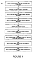
- FIG 1 is a flowchart 100 of one embodiment of a process that is used in the fabrication of a semiconductor device, specifically a monolithically integrated TMBS and MOSFET device, or SKYFET.
- a process of flowchart 100 is described in the context of a SKYFET such as that shown in Figure 10
- a subset of the process can be utilized to form only a TMBS device such as that shown in Figure 11 (that is, only the steps used to form the TMBS section of a SKYFET may be performed, in which case the steps used to form the MOSFET section are not necessarily performed).
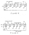
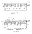
- Figure 1 is discussed in conjunction with Figures 2 through 9 , which are cross-sectional views showing selected stages in the fabrication of a semiconductor device according to an embodiment of the present invention, and also in conjunction with Figures 10 and 11 , which are top-down views of portions of embodiments of semiconductor devices that can be manufactured using the process of flowchart 100.
- a first mask 220 e.g., photoresist
- substrate 205 e.g., a p-type silicon substrate
- the trenches 210-215 are formed by etching the substrate 205 in areas not covered by the mask 220.
- the mask 220 is removed and the resulting structure is cleaned. Etching and sacrificial oxidation may follow the deaning to improve trench sidewall quality.
- a gate oxide layer 310 is grown in each of the trenches 210-215, and polysilicon 320 is deposited into each of the trenches 210-215. These steps may be followed by doping, blanket etch back, and polysilicon re-oxidation.
- the top surfaces of the regions of polysilicon 320 are recessed relative to the tops of the trenches 210-215. More specifically, the sidewalls of the trenches (or, correspondingly, the sidewalls of the mesas) have a height H1, while the polysilicon 320 is deposited within the trenches to a height H2, where H2 is less than H1.
- a second mask 410 is applied to define regions in which a body implant 420 (e.g., a p-body implant) is subsequently admitted.
- the mask 410 can then be stripped, the resulting structure can be cleaned, and the body implant 420 can be annealed and diffused to the desired junction depth.
- a third mask 510 is applied to define regions in which a source implant 520 (e.g., an n + source implant) is subsequently admitted.
- a source implant 520 e.g., an n + source implant
- the source implant 520 is not admitted into either the termination areas around the trenches 212 and 214 or the regions between the trenches 212-214, which correspond to the active region of a TMBS section of a SKYFET.
- the source implant 520 is permitted into the optional channel stopper (trench 215).
- the mask 510 can then be stripped and the resulting structure can be cleaned.
- a dielectric stack is deposited across the entire surface of the structure and densified.
- the dielectric stack includes a layer 610 of tetraethylorthosilicate (TEOS) and a layer 620 of borophosphosilicate glass (BPSG).
- TEOS tetraethylorthosilicate
- BPSG borophosphosilicate glass
- a fourth mask 710 is applied to define the contact openings 720, 721 and 722 in the active region of the MOSFET section(s) of the SKYFET. Because, prior to the etch, the upper surface of the structure is relatively flat, a thinner resist mask can be used.
- the source implant layer 520, the TEOS layer 610 and the BPSG layer 620 are etched, except for the areas under the mask 710, to form the contact openings 720-722.
- the active area of the TMBS section is masked by mask 710.
- the contact openings 720-722 permit contact between the n-type implants (layer 520) and the contact metal; however, the contact metal will not contact the regions of polysilicon 320. That is, the same metal does not contact both the source implants 520 and the polysilicon 320.
- the sidewalls of the trenches 210-215 are not exposed to the etch used to form the contact openings 720-722, thus avoiding the problem of encroachment of the contact metal (deposited in block 140) into the sidewalls of the trenches 210-215 and thereby eliminating or reducing edge leakage often attributed to such metal encroachment.
- the fourth mask 710 in order to contact the regions of polysilicon 320, the fourth mask 710 also defines contact openings in the gate pickup area (e.g., contacts 1010 and 1011) and in the polysilicon pickup area of the TMBS section (e.g., contact 1020). From the perspective of Figure 7 , for example, the polysilicon regions 320 extend a distance into the page, as shown in Figures 10 and 11 .
- the contacts 1010 and 1011 contact the polysilicon 320 that is in the MOSFET section, and the contact 1020 contacts the polysilicon 320 that is in the TMBS section.
- contact clamping implant and shallow contact implant are performed and the fourth mask 710 can be stripped.
- the contact clamping and shallow contact implants improve the contact resistance to the body and also shift avalanche breakdown from the trenches to the center of each mesa.
- the resulting structure can then be subjected to high temperature reflow in order to activate the contact implant, activate the source implant if it has not be activated, drive the source implant to its target junction depth, densify the dielectric stack if needed, and contour the dielectric stack if desired in order to soften the topography of the structure.
- a fifth mask 810 is used to pattern only the active area of the TMBS section, in order to etch away portions of the dielectric stack (e.g., TEOS layer 610 and BPSG layer 620) prior to deposition of barrier and contact metal.
- portions of the dielectric stack e.g., TEOS layer 610 and BPSG layer 620
- barrier and contact metal e.g., TEOS layer 610 and BPSG layer 620
- any remaining oxide layered on the surfaces of the mesas in the TMBS section e.g., mesas 820 and 821) is cleaned from those surfaces.
- the oxide on the TMBS mesa surfaces is dry etched to a thickness of approximately 1000 Angstroms, and then a buffered oxide etch (BOE) (e.g., a 9:1 BOE wet dip) is applied to remove any remaining oxide, so that good contact can be made between the mesa surfaces and the contact metal (deposited in block 140).
- BOE buffered oxide etch
- An objective of the wet overetch is to clean the oxide from the TMBS mesa surfaces, but not necessarily from inside the trenches 212-214.
- the top surface of the polysilicon 320 in trenches 212-214 remains recessed relative to the mesa surfaces 820-821, covered by a remaining thickness of the gate oxide layer 310.
- a source metal layer 910 is formed. More specifically, barrier and contact metal (e.g., titanium nitride, titanium, aluminum) is deposited to form the layer 910. The deposited metal can be subsequently patterned using a sixth mask (not shown). The source metal layer 910 contacts the TMBS mesas 820-821 but not the regions of polysilicon 320. That is, the source metal layer 910 is isolated from the polysilicon 320 by the oxide 310.
- barrier and contact metal e.g., titanium nitride, titanium, aluminum
- the source metal layer 910 contacts the TMBS mesas 820-821 but not the regions of polysilicon 320. That is, the source metal layer 910 is isolated from the polysilicon 320 by the oxide 310.
- a passivation layer if used, can be deposited and patterned using a seventh mask (not shown). The structure can then be ground and back metal can be applied.
- a device that includes only a TMBS section can be formed by skipping the steps described in blocks 115, 120 and 130, for example.
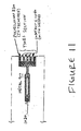
- Figures 10 and 11 show a top down view of a portion of a SKYFET device (including MOSFET sections and a TMBS section) and a similar view of a TMBS device, respectively, according to embodiments of the invention.
- the different regions of polysilicon 320 in the trenches of each MOSFET section are connected to each other and then to contacts 1010 and 1011 outside the active regions of the MOSFET section(s).
- the polysilicon 320 extends to the contacts 1010 and 1011, which are each beyond the edge of the source metal layer 910 that is disposed over the trenches 210-211 and 215 ( Figure 2 ) in the MOSFET sections that contain the polysilicon 320.
- electrical contact between the MOSFET polysilicon 320 and the gate metal is made via the contacts 1010 and 1011.
- contacts 1010 and 1011 are outside the active region of the MOSFET sections shown in Figure 10 . That is, contacts 1010 and 101 are outside the region of the source metal layer 910 that lies over the trenches in the MOSFET sections that contain the polysilicon 320.
- the different regions of polysilicon 320 in the trenches of each TMBS section are connected to each other and then to contact 1020, which is outside the active TMBS section of Figures 10 and 11 .
- the polysilicon 320 extends further than the mesas 820-821 ( Figure 8 ) in the lateral direction.
- the source metal layer 910 is disposed over the trenches 212-214 ( Figure 2 ) in the TMBS section that contain the polysilicon 320 and the mesas between those trenches.
- the source metal layer 910 is in electrical contact with the mesas but is isolated from the polysilicon 320 in the trenches.
- Contacts 1040 represent the connections between the Schottky contact metal (source metal layer 910) and the mesas 820-821 ( Figure 8 ) in the TMBS section of Figure 10 . Electrical contact between the polysilicon 320 and the source metal layer 910 is made via the contact 1020.
- contact 1020 is outside the active region of the TMBS section shown in Figures 10 and 11 . That is, contact 1020 is outside the region of the source metal layer 910 that lies over the trenches in the TMBS section that contain the polysilicon 320 and that also lies over the mesas between those trenches.
- MOSFET source contacts 1030 that provide electrical contact to the source implants 520 ( Figure 7 ).
- embodiments in accordance with the present invention resolve the problem of excessive leakage by employing remote contacts (e.g., contact 1020) to the polysilicon regions of a TMBS device, as well as to the polysilicon regions of TMBS section(s) and MOSFET section(s) of a SKYFET device.
- the polysilicon 320 is recessed relative to adjacent mesas.
- a stacked layer of TEOS 610 and BPSG 620 ( Figure 6 ) is employed to selectively leave a thin layer of oxide on top of the polysilicon 320 while making sure that the mesa surfaces in the TMBS section (e.g., mesas 820-821) are open for contact metal, but without exposing trench sidewalls to etching.
Landscapes
- Electrodes Of Semiconductors (AREA)
- Metal-Oxide And Bipolar Metal-Oxide Semiconductor Integrated Circuits (AREA)
- Insulated Gate Type Field-Effect Transistor (AREA)
Applications Claiming Priority (2)
| Application Number | Priority Date | Filing Date | Title |
|---|---|---|---|
| US92523707P | 2007-04-19 | 2007-04-19 | |
| US12/098,950 US8368126B2 (en) | 2007-04-19 | 2008-04-07 | Trench metal oxide semiconductor with recessed trench material and remote contacts |
Publications (2)
| Publication Number | Publication Date |
|---|---|
| EP1983576A2 true EP1983576A2 (fr) | 2008-10-22 |
| EP1983576A3 EP1983576A3 (fr) | 2009-09-23 |
Family
ID=39642673
Family Applications (1)
| Application Number | Title | Priority Date | Filing Date |
|---|---|---|---|
| EP08007591A Withdrawn EP1983576A3 (fr) | 2007-04-19 | 2008-04-18 | Dispositif métal-oxyde-semi-conducteur à tranchée et son procédé de fabrication |
Country Status (7)
| Country | Link |
|---|---|
| US (2) | US8368126B2 (fr) |
| EP (1) | EP1983576A3 (fr) |
| JP (1) | JP5197122B2 (fr) |
| KR (1) | KR101047947B1 (fr) |
| CN (1) | CN101295712B (fr) |
| MY (1) | MY147107A (fr) |
| TW (1) | TWI389312B (fr) |
Families Citing this family (14)
| Publication number | Priority date | Publication date | Assignee | Title |
|---|---|---|---|---|
| US8368126B2 (en) * | 2007-04-19 | 2013-02-05 | Vishay-Siliconix | Trench metal oxide semiconductor with recessed trench material and remote contacts |
| US10600902B2 (en) | 2008-02-13 | 2020-03-24 | Vishay SIliconix, LLC | Self-repairing field effect transisitor |
| US9306056B2 (en) | 2009-10-30 | 2016-04-05 | Vishay-Siliconix | Semiconductor device with trench-like feed-throughs |
| US8604525B2 (en) | 2009-11-02 | 2013-12-10 | Vishay-Siliconix | Transistor structure with feed-through source-to-substrate contact |
| JP5654818B2 (ja) * | 2010-09-27 | 2015-01-14 | ルネサスエレクトロニクス株式会社 | パワー系半導体装置の製造方法 |
| KR20120064364A (ko) * | 2010-12-09 | 2012-06-19 | 삼성전자주식회사 | 태양 전지의 제조 방법 |
| CN102569422B (zh) * | 2010-12-31 | 2015-08-26 | 比亚迪股份有限公司 | 一种肖特基整流器件及制造方法 |
| CN103151270A (zh) * | 2013-02-26 | 2013-06-12 | 上海宏力半导体制造有限公司 | 沟槽式金属氧化物半导体肖特基势垒器件制造方法 |
| CN104425628B (zh) * | 2013-08-22 | 2017-11-07 | 大中积体电路股份有限公司 | 半导体功率元件及其半导体结构 |
| CN103985627B (zh) * | 2014-05-12 | 2017-03-08 | 上海先进半导体制造股份有限公司 | 提高tmbs良率的工艺方法 |
| US9425304B2 (en) | 2014-08-21 | 2016-08-23 | Vishay-Siliconix | Transistor structure with improved unclamped inductive switching immunity |
| CN108766965B (zh) * | 2018-08-03 | 2023-06-13 | 淄博汉林半导体有限公司 | 一种漏极共用的沟槽式双mos管器件及制造方法 |
| CN115831759B (zh) * | 2023-02-22 | 2023-05-02 | 南京华瑞微集成电路有限公司 | 一种集成sbd结构的sgt mosfet及其制作方法 |
| CN119132948B (zh) * | 2024-08-22 | 2025-10-31 | 上海华虹宏力半导体制造有限公司 | 减小肖特基槽底台阶高度的方法 |
Citations (1)
| Publication number | Priority date | Publication date | Assignee | Title |
|---|---|---|---|---|
| EP1168455A2 (fr) * | 2000-06-30 | 2002-01-02 | Kabushiki Kaisha Toshiba | Element de commutation semiconducteur a puissance |
Family Cites Families (74)
| Publication number | Priority date | Publication date | Assignee | Title |
|---|---|---|---|---|
| JPS57206073A (en) | 1981-06-12 | 1982-12-17 | Hitachi Ltd | Mis semiconductor device |
| NL8302092A (nl) | 1983-06-13 | 1985-01-02 | Philips Nv | Halfgeleiderinrichting bevattende een veldeffekttransistor. |
| JPH0612828B2 (ja) | 1983-06-30 | 1994-02-16 | 株式会社東芝 | 半導体装置 |
| JPS60136378A (ja) | 1983-12-26 | 1985-07-19 | Hitachi Ltd | 半導体装置およびその製造方法 |
| US4837606A (en) | 1984-02-22 | 1989-06-06 | General Electric Company | Vertical MOSFET with reduced bipolar effects |
| JPS60196974A (ja) | 1984-03-19 | 1985-10-05 | Toshiba Corp | 導電変調型mosfet |
| GB2165090A (en) | 1984-09-26 | 1986-04-03 | Philips Electronic Associated | Improving the field distribution in high voltage semiconductor devices |
| JPS6239069A (ja) | 1985-08-13 | 1987-02-20 | Mitsubishi Electric Corp | 電界効果型半導体装置 |
| US4760431A (en) | 1985-09-30 | 1988-07-26 | Kabushiki Kaisha Toshiba | Gate turn-off thyristor with independent turn-on/off controlling transistors |
| US4779123A (en) | 1985-12-13 | 1988-10-18 | Siliconix Incorporated | Insulated gate transistor array |
| IT1204243B (it) | 1986-03-06 | 1989-03-01 | Sgs Microelettronica Spa | Procedimento autoallineato per la fabbricazione di celle dmos di piccole dimensioni e dispositivi mos ottenuti mediante detto procedimento |
| IT1213411B (it) | 1986-12-17 | 1989-12-20 | Sgs Microelettronica Spa | Struttura mos di potenza con dispositivo di protezione contro le sovratensioni e processo per lasua fabbricazione. |
| US4775879A (en) | 1987-03-18 | 1988-10-04 | Motorola Inc. | FET structure arrangement having low on resistance |
| JPS63252480A (ja) | 1987-04-09 | 1988-10-19 | Mitsubishi Electric Corp | 縦形モス電界効果トランジスタ |
| US5283201A (en) | 1988-05-17 | 1994-02-01 | Advanced Power Technology, Inc. | High density power device fabrication process |
| US5072266A (en) | 1988-12-27 | 1991-12-10 | Siliconix Incorporated | Trench DMOS power transistor with field-shaping body profile and three-dimensional geometry |
| DE69029180T2 (de) | 1989-08-30 | 1997-05-22 | Siliconix Inc | Transistor mit Spannungsbegrenzungsanordnung |
| US5326711A (en) | 1993-01-04 | 1994-07-05 | Texas Instruments Incorporated | High performance high voltage vertical transistor and method of fabrication |
| US5410170A (en) | 1993-04-14 | 1995-04-25 | Siliconix Incorporated | DMOS power transistors with reduced number of contacts using integrated body-source connections |
| JPH07122749A (ja) | 1993-09-01 | 1995-05-12 | Toshiba Corp | 半導体装置及びその製造方法 |
| JPH07294961A (ja) | 1994-04-22 | 1995-11-10 | Semiconductor Energy Lab Co Ltd | アクティブマトリクス型表示装置の駆動回路および設計方法 |
| JP3338178B2 (ja) | 1994-05-30 | 2002-10-28 | 株式会社東芝 | 半導体装置およびその製造方法 |
| JP3291958B2 (ja) | 1995-02-21 | 2002-06-17 | 富士電機株式会社 | バックソースmosfet |
| US6049108A (en) | 1995-06-02 | 2000-04-11 | Siliconix Incorporated | Trench-gated MOSFET with bidirectional voltage clamping |
| JP3850054B2 (ja) | 1995-07-19 | 2006-11-29 | 三菱電機株式会社 | 半導体装置 |
| US6133587A (en) | 1996-01-23 | 2000-10-17 | Denso Corporation | Silicon carbide semiconductor device and process for manufacturing same |
| US5742076A (en) | 1996-06-05 | 1998-04-21 | North Carolina State University | Silicon carbide switching devices having near ideal breakdown voltage capability and ultralow on-state resistance |
| DE69739206D1 (de) | 1996-07-19 | 2009-02-26 | Siliconix Inc | Hochdichte-graben-dmos-transistor mit grabenbodemimplantierung |
| US6057558A (en) | 1997-03-05 | 2000-05-02 | Denson Corporation | Silicon carbide semiconductor device and manufacturing method thereof |
| US5864158A (en) | 1997-04-04 | 1999-01-26 | Advanced Micro Devices, Inc. | Trench-gated vertical CMOS device |
| US6346438B1 (en) | 1997-06-30 | 2002-02-12 | Kabushiki Kaisha Toshiba | Method of manufacturing a semiconductor device |
| US20010003367A1 (en) | 1998-06-12 | 2001-06-14 | Fwu-Iuan Hshieh | Trenched dmos device with low gate charges |
| US6621121B2 (en) | 1998-10-26 | 2003-09-16 | Silicon Semiconductor Corporation | Vertical MOSFETs having trench-based gate electrodes within deeper trench-based source electrodes |
| US5998833A (en) | 1998-10-26 | 1999-12-07 | North Carolina State University | Power semiconductor devices having improved high frequency switching and breakdown characteristics |
| US6351018B1 (en) * | 1999-02-26 | 2002-02-26 | Fairchild Semiconductor Corporation | Monolithically integrated trench MOSFET and Schottky diode |
| US6413822B2 (en) | 1999-04-22 | 2002-07-02 | Advanced Analogic Technologies, Inc. | Super-self-aligned fabrication process of trench-gate DMOS with overlying device layer |
| US6211018B1 (en) | 1999-08-14 | 2001-04-03 | Electronics And Telecommunications Research Institute | Method for fabricating high density trench gate type power device |
| JP2001085685A (ja) | 1999-09-13 | 2001-03-30 | Shindengen Electric Mfg Co Ltd | トランジスタ |
| US7186609B2 (en) * | 1999-12-30 | 2007-03-06 | Siliconix Incorporated | Method of fabricating trench junction barrier rectifier |
| US6407435B1 (en) * | 2000-02-11 | 2002-06-18 | Sharp Laboratories Of America, Inc. | Multilayer dielectric stack and method |
| US6838735B1 (en) * | 2000-02-24 | 2005-01-04 | International Rectifier Corporation | Trench FET with non overlapping poly and remote contact therefor |
| US6246090B1 (en) | 2000-03-14 | 2001-06-12 | Intersil Corporation | Power trench transistor device source region formation using silicon spacer |
| JP3910335B2 (ja) | 2000-03-22 | 2007-04-25 | セイコーインスツル株式会社 | 縦形mosトランジスタ及びその製造方法 |
| GB0010041D0 (en) | 2000-04-26 | 2000-06-14 | Koninkl Philips Electronics Nv | Trench semiconductor device manufacture |
| EP1170803A3 (fr) | 2000-06-08 | 2002-10-09 | Siliconix Incorporated | MOSFET à grille en tranchée et sa méthode de fabrication |
| US6593620B1 (en) * | 2000-10-06 | 2003-07-15 | General Semiconductor, Inc. | Trench DMOS transistor with embedded trench schottky rectifier |
| US6586833B2 (en) | 2000-11-16 | 2003-07-01 | Silicon Semiconductor Corporation | Packaged power devices having vertical power mosfets therein that are flip-chip mounted to slotted gate electrode strip lines |
| JP2002203966A (ja) * | 2000-12-27 | 2002-07-19 | Toshiba Corp | 半導体装置 |
| JP2002270840A (ja) | 2001-03-09 | 2002-09-20 | Toshiba Corp | パワーmosfet |
| JP4852792B2 (ja) | 2001-03-30 | 2012-01-11 | 株式会社デンソー | 半導体装置の製造方法 |
| JP4421144B2 (ja) | 2001-06-29 | 2010-02-24 | 株式会社東芝 | 半導体装置 |
| US6569738B2 (en) | 2001-07-03 | 2003-05-27 | Siliconix, Inc. | Process for manufacturing trench gated MOSFET having drain/drift region |
| US6882000B2 (en) | 2001-08-10 | 2005-04-19 | Siliconix Incorporated | Trench MIS device with reduced gate-to-drain capacitance |
| US7045859B2 (en) * | 2001-09-05 | 2006-05-16 | International Rectifier Corporation | Trench fet with self aligned source and contact |
| DE10212144B4 (de) | 2002-03-19 | 2005-10-06 | Infineon Technologies Ag | Transistoranordnung mit einer Struktur zur elektrischen Kontaktierung von Elektroden einer Trench-Transistorzelle |
| US6838722B2 (en) | 2002-03-22 | 2005-01-04 | Siliconix Incorporated | Structures of and methods of fabricating trench-gated MIS devices |
| DE10239310B4 (de) | 2002-08-27 | 2005-11-03 | Infineon Technologies Ag | Verfahren zur Herstellung einer elektrisch leitenden Verbindung zwischen einer ersten und einer zweiten vergrabenen Halbleiterschicht |
| TW588460B (en) | 2003-01-24 | 2004-05-21 | Ind Tech Res Inst | Trench power MOSFET and method of making the same |
| JP2004241413A (ja) * | 2003-02-03 | 2004-08-26 | Toshiba Corp | 半導体装置 |
| US6919248B2 (en) | 2003-03-14 | 2005-07-19 | International Rectifier Corporation | Angled implant for shorter trench emitter |
| JP3964819B2 (ja) | 2003-04-07 | 2007-08-22 | 株式会社東芝 | 絶縁ゲート型半導体装置 |
| US6974750B2 (en) | 2003-06-11 | 2005-12-13 | International Rectifier Corporation | Process for forming a trench power MOS device suitable for large diameter wafers |
| JP3703816B2 (ja) * | 2003-06-18 | 2005-10-05 | 株式会社東芝 | 半導体装置 |
| GB0314392D0 (en) * | 2003-06-20 | 2003-07-23 | Koninkl Philips Electronics Nv | Trench mos structure |
| US6987305B2 (en) * | 2003-08-04 | 2006-01-17 | International Rectifier Corporation | Integrated FET and schottky device |
| US7279743B2 (en) | 2003-12-02 | 2007-10-09 | Vishay-Siliconix | Closed cell trench metal-oxide-semiconductor field effect transistor |
| JP4829473B2 (ja) * | 2004-01-21 | 2011-12-07 | オンセミコンダクター・トレーディング・リミテッド | 絶縁ゲート型半導体装置およびその製造方法 |
| US20050199918A1 (en) * | 2004-03-15 | 2005-09-15 | Daniel Calafut | Optimized trench power MOSFET with integrated schottky diode |
| US6906380B1 (en) | 2004-05-13 | 2005-06-14 | Vishay-Siliconix | Drain side gate trench metal-oxide-semiconductor field effect transistor |
| JP2006012967A (ja) | 2004-06-23 | 2006-01-12 | Toshiba Corp | 半導体装置 |
| US20060273390A1 (en) * | 2005-06-06 | 2006-12-07 | M-Mos Sdn. Bhd. | Gate contact and runners for high density trench MOSFET |
| JP2007299970A (ja) * | 2006-05-01 | 2007-11-15 | Toshiba Corp | 半導体装置及びその製造方法 |
| US8368126B2 (en) * | 2007-04-19 | 2013-02-05 | Vishay-Siliconix | Trench metal oxide semiconductor with recessed trench material and remote contacts |
| CN101868856B (zh) * | 2007-09-21 | 2014-03-12 | 飞兆半导体公司 | 用于功率器件的超结结构及制造方法 |
-
2008
- 2008-04-07 US US12/098,950 patent/US8368126B2/en active Active
- 2008-04-17 TW TW097113917A patent/TWI389312B/zh active
- 2008-04-18 MY MYPI20081154A patent/MY147107A/en unknown
- 2008-04-18 JP JP2008108751A patent/JP5197122B2/ja active Active
- 2008-04-18 KR KR1020080036192A patent/KR101047947B1/ko active Active
- 2008-04-18 EP EP08007591A patent/EP1983576A3/fr not_active Withdrawn
- 2008-04-21 CN CN2008100904941A patent/CN101295712B/zh active Active
-
2012
- 2012-12-27 US US13/728,997 patent/US8883580B2/en active Active
Patent Citations (1)
| Publication number | Priority date | Publication date | Assignee | Title |
|---|---|---|---|---|
| EP1168455A2 (fr) * | 2000-06-30 | 2002-01-02 | Kabushiki Kaisha Toshiba | Element de commutation semiconducteur a puissance |
Also Published As
| Publication number | Publication date |
|---|---|
| KR101047947B1 (ko) | 2011-07-12 |
| TWI389312B (zh) | 2013-03-11 |
| JP5197122B2 (ja) | 2013-05-15 |
| KR20080094617A (ko) | 2008-10-23 |
| US8368126B2 (en) | 2013-02-05 |
| EP1983576A3 (fr) | 2009-09-23 |
| CN101295712A (zh) | 2008-10-29 |
| JP2008270811A (ja) | 2008-11-06 |
| US20080258212A1 (en) | 2008-10-23 |
| US8883580B2 (en) | 2014-11-11 |
| US20140235023A1 (en) | 2014-08-21 |
| CN101295712B (zh) | 2012-06-06 |
| TW200901469A (en) | 2009-01-01 |
| MY147107A (en) | 2012-10-31 |
Similar Documents
| Publication | Publication Date | Title |
|---|---|---|
| US8368126B2 (en) | Trench metal oxide semiconductor with recessed trench material and remote contacts | |
| US10685955B2 (en) | Trench diode and method of forming the same | |
| US9735266B2 (en) | Self-aligned contact for trench MOSFET | |
| US8241978B2 (en) | Method of manufacturing semiconductor device having integrated MOSFET and Schottky diode | |
| US20190273152A1 (en) | Method of manufacturing shielded gate trench mosfet devices | |
| US20110233659A1 (en) | Semiconductor power device and manufacturing method thereof | |
| CN109872974B (zh) | 具有集成pn二极管温度传感器的半导体器件 | |
| CN105226020A (zh) | 含功率晶体管单元和横向晶体管的半导体器件及制造方法 | |
| US6800509B1 (en) | Process for enhancement of voltage endurance and reduction of parasitic capacitance for a trench power MOSFET | |
| US8017494B2 (en) | Termination trench structure for mosgated device and process for its manufacture | |
| US20150255565A1 (en) | High density mosfet array with self-aligned contacts enhancement plug and method | |
| CN113519054A (zh) | 制造屏蔽栅极沟槽mosfet装置的方法 | |
| US20090166731A1 (en) | Vertical-type field-effect transistor and manufacturing method thereof | |
| CN114284149B (zh) | 一种屏蔽栅沟槽场效应晶体管的制备方法 | |
| US12199091B2 (en) | Shallow trench isolation processing with local oxidation of silicon | |
| CN110957370A (zh) | 横向双扩散晶体管的制造方法 | |
| US12051745B2 (en) | Manufacturing method of a semiconductor device | |
| CN106935645B (zh) | 具有底部栅极的金氧半场效晶体管功率元件 | |
| US20250120209A1 (en) | Image sensor device and method of manufacturing the same | |
| US8227858B2 (en) | Power MOSFET | |
| JP2011101018A (ja) | トレンチ金属酸化物半導体電界効果トランジスタの製造方法 | |
| US7741693B1 (en) | Method for integrating trench MOS Schottky barrier devices into integrated circuits and related semiconductor devices | |
| US11949010B2 (en) | Metal oxide semiconductor device and method for manufacturing the same | |
| CN222356845U (zh) | 一种功率半导体器件 | |
| CN222692196U (zh) | 一种功率半导体器件 |
Legal Events
| Date | Code | Title | Description |
|---|---|---|---|
| PUAI | Public reference made under article 153(3) epc to a published international application that has entered the european phase |
Free format text: ORIGINAL CODE: 0009012 |
|
| AK | Designated contracting states |
Kind code of ref document: A2 Designated state(s): AT BE BG CH CY CZ DE DK EE ES FI FR GB GR HR HU IE IS IT LI LT LU LV MC MT NL NO PL PT RO SE SI SK TR |
|
| AX | Request for extension of the european patent |
Extension state: AL BA MK RS |
|
| PUAL | Search report despatched |
Free format text: ORIGINAL CODE: 0009013 |
|
| AK | Designated contracting states |
Kind code of ref document: A3 Designated state(s): AT BE BG CH CY CZ DE DK EE ES FI FR GB GR HR HU IE IS IT LI LT LU LV MC MT NL NO PL PT RO SE SI SK TR |
|
| AX | Request for extension of the european patent |
Extension state: AL BA MK RS |
|
| RIC1 | Information provided on ipc code assigned before grant |
Ipc: H01L 29/45 20060101ALN20080801BHEP Ipc: H01L 29/872 20060101ALI20090814BHEP Ipc: H01L 21/329 20060101ALI20090814BHEP Ipc: H01L 21/336 20060101ALI20090814BHEP Ipc: H01L 29/78 20060101AFI20080801BHEP |
|
| 17P | Request for examination filed |
Effective date: 20100316 |
|
| AKX | Designation fees paid |
Designated state(s): AT BE BG CH CY CZ DE DK EE ES FI FR GB GR HR HU IE IS IT LI LT LU LV MC MT NL NO PL PT RO SE SI SK TR |
|
| 17Q | First examination report despatched |
Effective date: 20101112 |
|
| STAA | Information on the status of an ep patent application or granted ep patent |
Free format text: STATUS: THE APPLICATION HAS BEEN WITHDRAWN |
|
| 18W | Application withdrawn |
Effective date: 20130308 |