EP1993137A2 - Méthode pour la fabrication d'un dispositif à l'état solide pour la prise d'image - Google Patents
Méthode pour la fabrication d'un dispositif à l'état solide pour la prise d'image Download PDFInfo
- Publication number
- EP1993137A2 EP1993137A2 EP08162529A EP08162529A EP1993137A2 EP 1993137 A2 EP1993137 A2 EP 1993137A2 EP 08162529 A EP08162529 A EP 08162529A EP 08162529 A EP08162529 A EP 08162529A EP 1993137 A2 EP1993137 A2 EP 1993137A2
- Authority
- EP
- European Patent Office
- Prior art keywords
- region
- layer
- semiconductor region
- control electrode
- mos transistor
- Prior art date
- Legal status (The legal status is an assumption and is not a legal conclusion. Google has not performed a legal analysis and makes no representation as to the accuracy of the status listed.)
- Withdrawn
Links
Images



Classifications
-
- H—ELECTRICITY
- H10—SEMICONDUCTOR DEVICES; ELECTRIC SOLID-STATE DEVICES NOT OTHERWISE PROVIDED FOR
- H10F—INORGANIC SEMICONDUCTOR DEVICES SENSITIVE TO INFRARED RADIATION, LIGHT, ELECTROMAGNETIC RADIATION OF SHORTER WAVELENGTH OR CORPUSCULAR RADIATION
- H10F39/00—Integrated devices, or assemblies of multiple devices, comprising at least one element covered by group H10F30/00, e.g. radiation detectors comprising photodiode arrays
- H10F39/80—Constructional details of image sensors
- H10F39/803—Pixels having integrated switching, control, storage or amplification elements
- H10F39/8033—Photosensitive area
-
- H—ELECTRICITY
- H10—SEMICONDUCTOR DEVICES; ELECTRIC SOLID-STATE DEVICES NOT OTHERWISE PROVIDED FOR
- H10F—INORGANIC SEMICONDUCTOR DEVICES SENSITIVE TO INFRARED RADIATION, LIGHT, ELECTROMAGNETIC RADIATION OF SHORTER WAVELENGTH OR CORPUSCULAR RADIATION
- H10F39/00—Integrated devices, or assemblies of multiple devices, comprising at least one element covered by group H10F30/00, e.g. radiation detectors comprising photodiode arrays
- H10F39/011—Manufacture or treatment of image sensors covered by group H10F39/12
- H10F39/014—Manufacture or treatment of image sensors covered by group H10F39/12 of CMOS image sensors
-
- H—ELECTRICITY
- H10—SEMICONDUCTOR DEVICES; ELECTRIC SOLID-STATE DEVICES NOT OTHERWISE PROVIDED FOR
- H10F—INORGANIC SEMICONDUCTOR DEVICES SENSITIVE TO INFRARED RADIATION, LIGHT, ELECTROMAGNETIC RADIATION OF SHORTER WAVELENGTH OR CORPUSCULAR RADIATION
- H10F39/00—Integrated devices, or assemblies of multiple devices, comprising at least one element covered by group H10F30/00, e.g. radiation detectors comprising photodiode arrays
- H10F39/10—Integrated devices
- H10F39/12—Image sensors
- H10F39/18—Complementary metal-oxide-semiconductor [CMOS] image sensors; Photodiode array image sensors
-
- H—ELECTRICITY
- H10—SEMICONDUCTOR DEVICES; ELECTRIC SOLID-STATE DEVICES NOT OTHERWISE PROVIDED FOR
- H10F—INORGANIC SEMICONDUCTOR DEVICES SENSITIVE TO INFRARED RADIATION, LIGHT, ELECTROMAGNETIC RADIATION OF SHORTER WAVELENGTH OR CORPUSCULAR RADIATION
- H10F39/00—Integrated devices, or assemblies of multiple devices, comprising at least one element covered by group H10F30/00, e.g. radiation detectors comprising photodiode arrays
- H10F39/80—Constructional details of image sensors
- H10F39/803—Pixels having integrated switching, control, storage or amplification elements
-
- H—ELECTRICITY
- H10—SEMICONDUCTOR DEVICES; ELECTRIC SOLID-STATE DEVICES NOT OTHERWISE PROVIDED FOR
- H10F—INORGANIC SEMICONDUCTOR DEVICES SENSITIVE TO INFRARED RADIATION, LIGHT, ELECTROMAGNETIC RADIATION OF SHORTER WAVELENGTH OR CORPUSCULAR RADIATION
- H10F77/00—Constructional details of devices covered by this subclass
- H10F77/10—Semiconductor bodies
- H10F77/14—Shape of semiconductor bodies; Shapes, relative sizes or dispositions of semiconductor regions within semiconductor bodies
- H10F77/147—Shapes of bodies
-
- Y—GENERAL TAGGING OF NEW TECHNOLOGICAL DEVELOPMENTS; GENERAL TAGGING OF CROSS-SECTIONAL TECHNOLOGIES SPANNING OVER SEVERAL SECTIONS OF THE IPC; TECHNICAL SUBJECTS COVERED BY FORMER USPC CROSS-REFERENCE ART COLLECTIONS [XRACs] AND DIGESTS
- Y02—TECHNOLOGIES OR APPLICATIONS FOR MITIGATION OR ADAPTATION AGAINST CLIMATE CHANGE
- Y02E—REDUCTION OF GREENHOUSE GAS [GHG] EMISSIONS, RELATED TO ENERGY GENERATION, TRANSMISSION OR DISTRIBUTION
- Y02E10/00—Energy generation through renewable energy sources
- Y02E10/50—Photovoltaic [PV] energy
Definitions
- the present invention relates to a solid state image pickup device and a method for manufacturing the same.
- CCD sensor consisting of photodiodes and CCD shift registers
- CMOS sensor such as APS (active pixel sensor) consisting of photodiodes and MOS transistors.
- the APS is provided, in each pixel, with a photodiode, an MOS switch, an amplifier circuit for amplifying the signal from the photodiode etc., and has various advantages of enabling XY addressing and single-chip integration of the sensor and the signal processing circuit.
- the APS is associated with a smaller pixel aperture rate and difficulty in reducing the chip size which determines the dimension of the optical system, and, for these reasons, the majority of the commercially available solid state image pickup devices is represented by the CCD.
- CMOS sensor is recently attracting attention, because of the progress in the technology for size reduction of the MOS transistors and the increasing demand for the single-chip integration of the sensor and the signal processing circuit and for the lower electric power consumption.
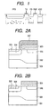
- Fig. 1 is an equivalent circuit diagram of a pixel region of the conventional APS and a solid state image pickup device utilizing the same, as reported by Eric R. Fossum et al. at the 1995 IEEE Work Shop. In the following there will be briefly explained the configuration of the prior technology.
- the photoelectric conversion unit is composed of a buried photodiode of the type employed in the CCD.
- the buried photodiode with a surfacially highly doped p-layer can suppress the dark current generated at the SiO 2 surface, and there can also be formed a junction capacitance between the n-layer in the accumulation unit and the surfacial p-layer, thereby increasing the saturation charge amount of the photodiode.
- a photo-induced signal charge Q sig accumulated in a photoelectric conversion unit (photodiode) PPD is transferred, through a transfer unit TX consisting of a MOS transistor, to a floating diffusion region FD.
- the signal charge Q sig is converted by the capacitance C FD of the floating diffusion region into a voltage Q sig /C FD , which is read through a source follower circuit.
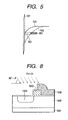
- Fig. 5 shows the potentials of the channel region in a conventional MOS transistor and the transferring MOS transistor.
- the light enters from the left-hand side, and, on the right-hand side there are formed in succession a transparent insulation layer such as of SiO 2 or SiN, a highly doped p-layer and an n-layer constituting the photodiode.
- the curve show changes in the potential level under the voltage application.
- an oxide layer 301 Fermi level 302 of the n-layer of the photodiode, Fermi level 303 of a bypass region, a potential 304 under the application of a threshold voltage of the present invention, and a potential 305 under the application of the threshold voltage of the prior technology.
- the potential has to be varied larger since the n-layer is separated from the surface.
- V th 2 ⁇ ⁇ F + V S * 2 ⁇ ⁇ Si * q ⁇ N sub C OX + 2 ⁇ ⁇ F + V S + V FB wherein:
- the threshold voltage of the ordinary MOS transistor is about 0.7 V while that of the buried source becomes as high as 5.0 V.
- the charge remains in the photodiode, thus forming a retentive image or a noise, thus significantly deteriorating the image quality.
- the object of the present invention is to provide a solid state image pickup device capable of efficiently transferring the charge accumulated in the photoelectric conversion element, and a manufacturing method therefor.
- a solid state image pickup device comprising a photoelectric conversion unit including a first region of a first conductive type formed on a semiconductor substrate having a main surface, a second region of a second conductive type formed in the first region, and a third region of the first conductive type formed between the second region and the main surface; a fourth region of the second conductive type formed in the first region; and a charge transfer unit including the first region, an insulation layer on the first region and a control electrode on the insulating layer, for transferring a signal charge accumulated in the photoelectric conversion unit to the fourth region; wherein the photoelectric conversion unit and the charge transfer unit are connected through a fifth region of the second conductive type.
- a method for forming a solid state image pickup device including at least (1) a photoelectric conversion unit including a first region of a first conductive type formed on a semiconductor substrate having a main surface, a second region of a second conductive type formed in the first region, and a third region of the first conductive type formed between the second region and the main surface, (2) a fourth region of the second conductive type formed in the first region, (3) a charge transfer unit including the first region, an insulation layer on the first region and a control electrode on the insulation layer, for transferring the signal charge accumulated in the photoelectric conversion unit to the fourth region, wherein the method comprising an ion implantation step of doping an impurity for forming the second conductive type into the second region, utilizing the control electrode of the charge transfer unit as a mask.
- a method for forming a solid state image pickup device comprising a photoelectric conversion unit including a first region of a first conductive type formed on a semiconductor substrate having a main surface, a second region of a second conductive type formed in the first region, and a third region of the first conductive type formed between the second region and the main surface; a fourth region of the second conductive type formed in the first region; and a charge transfer unit including the first region, an insulation layer on the first region and a control electrode on the insulation layer, for transferring the signal charge accumulated in the photoelectric conversion unit to the fourth region, wherein a fifth region of the second conductive type is formed between the photoelectric conversion unit and the charge transfer unit.
- an region of a conductive type same as that of the charge accumulation layer there is provided, between the photodiode and the transfer MOS transistor, an region of a conductive type same as that of the charge accumulation layer.
- an n-doped region In case of a photodiode consisting of a charge accumulation region formed in a p-well and a surfacially highly doped p-layer formed on the surface of the charge accumulation region, there is provided an n-doped region.
- Such the region is hereinafter called a bypass region.
- the electrons in the charge accumulation region move to the floating diffusion region through the bypass region of the low potential and the surface of the transfer MOS transistor, whereby the threshold voltage thereof can be made lower than in the prior art.
- bypass region consisting of a surfacially highly doped p-layer 505 is prepared for example by forming a resist layer 507 as shown in Fig. 2A .
- Figs. 2A and 2B there are shown an n-type substrate 501, a p-well 502, a CCD vertical transfer electrode 503, an n-layer 504 constituting the photodiode, and a CCD vertical register 506.
- the bypass region is required to meet the following conditions:
- the conditions (1) and (2) respectively determine the lower limit and the upper limit of the impurity concentration and the width of the bypass region. If the impurity concentration of the substrate increase as a result of pixel size reduction, the margin for the impurity concentration and the width of the bypass region is inevitably reduced.
- the configuration of the present embodiment has the following features:
- the lines of electric force from the drain region can be made to influence the photodiode, thereby assisting the extraction of electrons from the charge accumulation layer.
- the photoelectric conversion element (photodiode) is obtained by forming a p-well 102 on an n-type substrate 101, then forming an n-layer 104 in the p-well 102, and forming a p-layer 105 with a highly doped surface on the n-layer 104.
- a floating diffusion region FD 107 is obtained by forming an n-layer 107 in the p-well 102.
- a gate region 103 of the transfer MOS transistor is formed above the region between the photodiode and the floating diffusion region 107 across an insulation layer, and, between the photodiode and the floating diffusion region FD 107 there is formed a bypass region continued from the n-layer of the photodiode.
- a floating diffusion region FD 107 is connected to the gate of an amplifying MOS transistor of an output circuit, while the source of the amplifying MOS transistor is connected to the drain of a line selecting switch MOS transistor 111, of which source is connected to a current source I 112 constituting the load of the amplifying MOS transistor, whereby a source follower amplifying circuit is constituted.
- the floating diffusion region FD 107 is also connected to the source of a resetting MOS transistor for setting the floating diffusion region FD, and the drain of the resetting MOS transistor is connected to a resetting power source 109.
- the transfer MOS transistor In response to the incident light, the electrons generated by photoelectric conversion are accumulated in the n-layer of the photodiode. In this state, the transfer MOS transistor is in the turned-off state. After the lapse of a predetermined accumulation time, a positive voltage is applied to the control electrode (gate region) of the transfer MOS transistor, thereby turning on the same and transferring the charge accumulated in the n-layer of the photodiode to the floating diffusion region. Before the transfer MOS transistor is turned on, the floating diffusion region is reset to a predetermined potential.
- the potential is lowered by Q sig /C FD from the reset potential, wherein Q sig is the transferred charge and C FD is the floating diffusion capacitance. If the charge accumulation layer of the photodiode is p-type, the voltage is elevated because the transferred charge consists of positive holes.
- the n-layer of the photodiode is given an inverse bias VFD sig1 with respect to the ground potential of the p-well and the surfacially highly doped p-layer, wherein VFD Sig1 is the voltage of the floating diffusion region lowered by Q sig /C FD from the reset voltage after the signal reading.
- VFD Sig1 is the voltage of the floating diffusion region lowered by Q sig /C FD from the reset voltage after the signal reading.
- a depletion layer extends from the p-well and the surfacially highly doped p-layer to the n-layer to deplete the entire n-layer of the photodiode, whereby the signal charge can be read to the floating diffusion region, almost without the remaining signal charge in the photodiode.
- the final output from the integrated circuit formed as the region sensor further includes a noise ⁇ V n2 of the read-out system after the output circuit for each pixel.
- V dep means a voltage at which the entire n-layers starts to be depleted.
- the depletion voltage of the photodiode generally means an inverse bias voltage realizing a condition: Number of accumulated charges in the accumulation unit ⁇ net number of impurities.
- the remaining signal level should be sufficiently smaller than the aforementioned noises ⁇ V n1 , ⁇ V n2 .
- the present invention utilizes the bypass region 106 between the buried photodiode and the transfer MOS transistor.
- the bypass region need not necessarily be in contact with the semiconductor surface, as shown in Fig. 4 . Because, the bypass region is provided between the n-layer of the photodiode and the channel of the transfer MOS transistor, and, being a buried channel, it need not reach the surface.
- the bypass region desirably reach the surfacial channel, but, even if it does not reach the surfacial channel, there can be obtained a transfer MOS transistor with a sufficiently lower threshold voltage in comparison with that in the prior art, according to the aforementioned equations.
- bypass region is present under the gate of the transfer MOS transistor.
- the potential under the gate is pushed up, and this effect is also applied to the bypass region, thereby further reducing the potential.
- the present embodiment is featured by a configuration in which the transfer MOS transistor is connected to the floating diffusion region, and the present inventors have found that this configuration provides following effects:
- each pixel contains many transistors, the transistors themselves have to be made smaller for reducing the pixel size, thus inevitably resulting in an elevated impurity concentration of the wells of the photodiode and the transfer MOS transistor. Also the power supply voltage has to be lowered in reducing the size of the transistors.
- the depletion voltage V dep while maintaining a constant amount of charge processed in the photodiode, it is necessary to design the accumulation layer (n-layer in Fig. 3 ) of the photodiode with a higher impurity concentration and with a smaller thickness. Also it is necessary to reduce the width of the bypass region since it has to be depleted together with the n-layer of the photodiode.
- the width of the bypass region being in the direction along the surface of the silicon substrate and generally less precise than the dimension in depth, constitutes a major factor in the deterioration of the production yield.
- the present invention increases the tolerance of the width of the bypass region by the above-mentioned effect (3), thereby improving the production yield.
- the present invention also allows to increase the production yield, by improving the working precision of the width of the bypass region, through the manufacturing process to be explained in the following.
- the bypass region in the conventional CCD has a significantly fluctuating width, depending on the aligning accuracy of the exposure apparatus, since it is formed by ion implantation of the n-layer of the photodiode prior to the formation of the control electrode of the transfer MOS transistor and ion implantation of the surfacially highly doped p-layer, utilizing the control electrode of the transfer MOS transistor as a mask.
- the present embodiment can improve the dimensional precision, since the bypass region is formed by ion implantation, utilizing the control electrode of the transfer MOS transistor as a mask.
- FIG. 6A to 6D for explaining a second embodiment of the present invention, relating to a method of forming the solid state image pickup device explained in the first embodiment.
- the photodiode and the peripheral configuration were formed in the following manner.
- n-type substrate 901 Boron was introduced by ion implantation into an n-type substrate 901, which was heat treated to form a p-well 902 with a surfacial impurity concentration of ca. 2 ⁇ 10 16 cm -3 . Then a photoresist layer 908 was formed and an n-layer 904 of the photodiode was obtained ( Fig. 6A ).
- a gate oxide layer 910 of a thickness of 30 nm was formed on the entire substrate surface by thermal oxidation, and a control electrode 903 of the transfer MOS transistor was formed ( Fig. 6B ).
- a photoresist layer 909 was formed on the photodiode and a part of the control electrode on the substrate surface, and, after a heat treatment of 950°C/20 min. in nitrogen atmosphere, a surfacially highly doped p-layer 905 was formed, utilizing the control electrode 903 as a mask ( Fig. 6C ).
- a first interlayer insulation layer, a contact, a first metal wiring, a second interlayer insulation layer, a via connecting the first and second metal wirings, a second metal wiring and a passivation layer were formed one after another according to an ordinary semiconductor process.
- the threshold voltage of an ordinary MOS transistor having highly doped n-type diffusion layers on both sides thereof, the threshold voltage of a transfer MOS transistor having a source consisting of a buried n-layer without the bypass region and the threshold voltage with the bypass region (configuration of the present invention) were respectively evaluated as 0.7 V, 2.2 V and 0.7 V. These results indicate that the threshold voltage is lowered to the level of the ordinary MOS transistor. The reduction in the threshold voltage widens the dynamic range of the floating diffusion region by at least 1.5 V.
- FIG. 7A to 7D for explaining a third embodiment of the present invention, relating to a method of forming the solid state image pickup device explained in the first embodiment.
- the photodiode and the peripheral configuration were formed in the following manner.
- n-type substrate 601 Boron was introduced by ion implantation into an n-type substrate 601, which was heat treated to form a p-well 602 with a surfacial impurity concentration of ca. 4 x 10 16 cm -3 .
- a gate oxide layer 610 of a thickness of 15 nm by thermal oxidation polycrystalline silicon was deposited with a thickness of 400 nm, thereby forming a control electrode 603 of the transfer MOS transistor ( Fig. 7A ).
- phosphor ions were implanted under 100 keV, utilizing a photoresist layer 608 and the control electrode 603.
- the projection stroke and standard deviation of phosphor were respectively 120 and 45 nm, whereby the polycrystalline silicon served satisfactorily as a mask ( Fig. 7B ).
- an As floating diffusion region 607 was formed by an ordinary semiconductor process ( Fig. 7D ). In this operation there were formed source and drain regions of the ordinary MOS transistor. In Fig. 7D , 606 indicates a bypass region.
- a first interlayer insulation layer, a contact, a first metal wiring, a second interlayer insulation layer, a via connecting the first and second metal wirings, a second metal wiring and a passivation layer were formed one after another according to an ordinary semiconductor process.
- FIG. 7A, 7B and 8 for explaining a fourth embodiment of the present invention, relating to a method of forming the solid state image pickup device explained in the first embodiment.
- the photodiode and the peripheral configuration were formed in the following manner.
- n-type substrate 601 Boron was introduced by ion implantation into an n-type substrate 601, which was heat treated to form a p-well 602 with a surfacial impurity concentration of ca. 4 x 10 16 cm -3 .
- a gate oxide layer 610 of a thickness of 15 nm by thermal oxidation polycrystalline silicon was deposited with a thickness of 400 nm, thereby forming a control electrode 603 of the transfer MOS transistor ( Fig. 7A ).
- oblique ion implantation of phosphor was conducted under 100 keV, utilizing a photoresist layer 1008 and the control electrode 1003 as the mask.
- the ion implantation angle ⁇ was selected as 20°. Because of such oblique ion implantation, the phosphor was present under the control electrode 1003 even immediately after the ion implantation.
- the projection stroke and standard deviation of phosphor were respectively 120 and 45 nm, whereby the polycrystalline silicon served satisfactorily as a mask ( Fig. 8 ).
- Fig. 8 there are also shown an n-type substrate 1001, a p-well 1002, and an n-layer 1004 of the photodiode.
- a photoresist layer 609 was formed again, and ion implantation of BF 2 was conducted at 35 keV, utilizing the photoresist layer 609 and the control electrode 603 as a mask ( Fig. 7C ).
- 605 indicates a surfacially highly doped p-layer.
- a first interlayer insulation layer, a contact, a first metal wiring, a second interlayer insulation layer, a via connecting the first and second metal wirings, a second metal wiring and a passivation layer were formed one after another according to an ordinary semiconductor process.
- the thermal treatment of 20 minutes at 950°C employed in the example 2 for diffusing phosphor is omitted.
- the thermal treatment time in the semiconductor process could be shortened, so that the peripheral MOS transistors for signal processing could be reduced in size.
- the phosphor ion implantation is divided into a first ion implantation for forming the bypass region and a second ion implantation for forming the n-layer of the photodiode.
- the first ion implantation was conducted with an ion implantation angle of 45°, and under a voltage of 80 keV.
- the ion implantation angle was selected larger than 20° in order to position the peak in the vicinity of the surface and to secure the bypass region.
- the second ion implantation was conducted with an ion implantation angle of 7° and under a voltage of 90 keV, in order to control the depletion voltage of the p-layer of the photodiode.
- FIG. 9A to 9D for explaining a sixth embodiment of the present invention, relating to a method of forming the solid state image pickup device explained in the first embodiment.
- the photodiode and the peripheral configuration were formed in the following manner.
- n-type substrate 1101 Boron was introduced by ion implantation into an n-type substrate 1101, which was heat treated to form a p-well 1102 with a surfacial impurity concentration of ca. 2 ⁇ 10 16 cm -3 , thereby forming the n-layer of the photodiode.
- a gate oxide layer 1110 of a thickness of 30 nm by thermal oxidation
- a control electrode 1103 of the transfer MOS transistor there was formed a control electrode 1103 of the transfer MOS transistor.
- phosphor ions were implanted under a voltage of 100 keV, utilizing a photoresist layer 1108 and the control electrode 1103 as the mask ( Fig. 9A ).
- 1104 indicates the n-layer of the photodiode.
- a side spacer 1111 was formed with a width of 150 nm.
- a photoresist layer 1109 was formed, and ion implantation of BF 2 was conducted at 35 keV, utilizing the photoresist layer 1109, the control electrode 1103 and the spacer as a mask.
- the ion implantation angle was selected as 7° in order to control channeling ( Fig. 9C ).
- 1105 indicates a surfacially highly doped p-layer.
- a first interlayer insulation layer, a contact, a first metal wiring, a second interlayer insulation film, a via connecting the first and second metal wirings, a second metal wiring and a passivation layer were formed one after another according to an ordinary semiconductor process.
- a bypass region 1106 of a width of about 150 nm As a result, there was formed a bypass region 1106 of a width of about 150 nm.
- the threshold voltage of an ordinary MOS transistor having highly doped n-type diffusion layers on both sides, the threshold voltage of a transfer MOS transistor having a source consisting of a buried n-layer without the bypass region and the threshold voltage with the bypass region (configuration of the present invention) were respectively evaluated as 0.7 V, 3.5 V and 0.7 V. These results indicate that the threshold voltage is lowered to the level of the ordinary MOS transistor.
- the above-mentioned side spacer corresponds to the mask means.
- the mask means may naturally be composed also by a silicide layer or the like instead of the side spacer.
- Figs. 7A, 7B , 8 and 10 for explaining a seventh embodiment of the present invention, relating to a method of forming the solid state image pickup device explained in the first embodiment.
- the photodiode and the peripheral configuration were formed in the following manner.
- n-type substrate 601 Boron was introduced by ion implantation into an n-type substrate 601, which was heat treated to form a p-well 602 with a surfacial impurity concentration of ca. 4 ⁇ 10 16 cm -3 .
- a gate oxide layer 610 of a thickness of 15 nm by thermal oxidation polycrystalline silicon was deposited with a thickness of 400 nm, thereby forming a control electrode 603 of the transfer MOS transistor ( Fig. 7A ).
- oblique ion implantation of phosphor was conducted under 100 keV, utilizing a photoresist layer 1008 and the control electrode 1003 a mask.
- the ion implantation angle ⁇ was selected as 10°. Because of such oblique ion implantation, the phosphor was present under the control electrode 1003 even immediately after the ion implantation.
- the projection stroke and standard deviation of phosphor were respectively 120 and 45 nm, whereby the polycrystalline silicon served satisfactorily as a mask ( Fig. 8 ).
- a photoresist layer 1209 was formed again, and ion implantation of BF 2 was conducted at 35 keV, utilizing the photoresist layer 1209 and the control electrode 1203 as a mask.
- the ion implantation angle was selected as -15° ( Fig. 10 ).
- Fig. 10 there are shown an n-type substrate 1201, a p-well 1202 and an n-layer 1204 of the photodiode.
- a floating diffusion region 607 including arsenic was formed by an ordinary semiconductor process ( Fig. 7D ). In this operation there were formed source and drain regions of the ordinary MOS transistor.
- a first interlayer insulation layer, a contact, a first metal wiring, a second interlayer insulation layer, a via connecting the first and second metal wirings, a second metal wiring and a passivation layer were formed one after another according to an ordinary semiconductor process.
- the thermal treatment of 20 minutes at 950°C employed in the example 2 for diffusing phosphor was omitted.
- the thermal treatment time in the semiconductor process could be shortened, so that the peripheral MOS transistors for signal processing could be reduced in size.
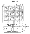
- the solid state image pickup device of the embodiment 1 or formed by methods explained in the second to eighth embodiments is an region sensor having a pixel configuration of Fig. 11 employing the photodiode 705 and the transfer MOS transistor, and also having a read-out circuit shown in Fig. 12 .
- a transfer switch Q1 consisting of a transfer MOS transistor for a photodiode 705
- a reset switch Q2 consisting of a reset MOS transistor for resetting the floating diffusion region
- an input MOS transistor Q3 of a source follower amplifying circuit consisting of a constant-current source 812, of which gate is connected to the floating diffusion region and which is connected as a load of the source side
- a selection switch Q4 for selecting the pixel to be read.
- Fig. 12 illustrates a solid state image pickup device, employing the pixel cells of the above-described photoelectric conversion elements, in a 3 x 3 matrix. There are shown a power supply line 801, a reset switch line 802, a selection switch line 806, a signal output line 804 and a transfer switch line 813.
- the light signal component is obtained by calculating the difference between the outputs 811, 811' to eliminate the resetting noise and the fixed pattern noise, thereby providing an image signal of a high S/N ratio.
- the foregoing embodiment allows to widen the dynamic range, by reducing the threshold value of the transfer MOS transistor, serving to transfer the photo-induced charge accumulated in the photodiode of the solid state image pickup device.
- the floating diffusion region of a bypass region capable of effectively transferring the charge accumulated by electrons or positive holes, the following advantages can be obtained:
Landscapes
- Solid State Image Pick-Up Elements (AREA)
- Light Receiving Elements (AREA)
- Facsimile Heads (AREA)
- Facsimile Scanning Arrangements (AREA)
Applications Claiming Priority (2)
| Application Number | Priority Date | Filing Date | Title |
|---|---|---|---|
| JP10070537A JPH11274454A (ja) | 1998-03-19 | 1998-03-19 | 固体撮像装置及びその形成方法 |
| EP99302095.7A EP0948056B9 (fr) | 1998-03-19 | 1999-03-18 | Dispositif de prise d'image à l'état solide et méthode pour sa fabrication |
Related Parent Applications (3)
| Application Number | Title | Priority Date | Filing Date |
|---|---|---|---|
| EP99302095.7A Division-Into EP0948056B9 (fr) | 1998-03-19 | 1999-03-18 | Dispositif de prise d'image à l'état solide et méthode pour sa fabrication |
| EP99302095.7A Division EP0948056B9 (fr) | 1998-03-19 | 1999-03-18 | Dispositif de prise d'image à l'état solide et méthode pour sa fabrication |
| EP99302095.7 Division | 1999-03-18 |
Publications (2)
| Publication Number | Publication Date |
|---|---|
| EP1993137A2 true EP1993137A2 (fr) | 2008-11-19 |
| EP1993137A3 EP1993137A3 (fr) | 2010-06-16 |
Family
ID=13434392
Family Applications (2)
| Application Number | Title | Priority Date | Filing Date |
|---|---|---|---|
| EP08162529A Withdrawn EP1993137A3 (fr) | 1998-03-19 | 1999-03-18 | Méthode pour la fabrication d'un dispositif à l'état solide pour la prise d'image |
| EP99302095.7A Expired - Lifetime EP0948056B9 (fr) | 1998-03-19 | 1999-03-18 | Dispositif de prise d'image à l'état solide et méthode pour sa fabrication |
Family Applications After (1)
| Application Number | Title | Priority Date | Filing Date |
|---|---|---|---|
| EP99302095.7A Expired - Lifetime EP0948056B9 (fr) | 1998-03-19 | 1999-03-18 | Dispositif de prise d'image à l'état solide et méthode pour sa fabrication |
Country Status (4)
| Country | Link |
|---|---|
| US (7) | US6661459B1 (fr) |
| EP (2) | EP1993137A3 (fr) |
| JP (1) | JPH11274454A (fr) |
| DE (1) | DE69940332D1 (fr) |
Families Citing this family (59)
| Publication number | Priority date | Publication date | Assignee | Title |
|---|---|---|---|---|
| JP4200545B2 (ja) * | 1998-06-08 | 2008-12-24 | ソニー株式会社 | 固体撮像素子およびその駆動方法、並びにカメラシステム |
| KR100384836B1 (ko) * | 1999-06-28 | 2003-05-22 | 주식회사 하이닉스반도체 | 이미지센서 및 그 제조방법 |
| US7324144B1 (en) * | 1999-10-05 | 2008-01-29 | Canon Kabushiki Kaisha | Solid image pickup device, image pickup system and method of driving solid image pickup device |
| JP3467013B2 (ja) | 1999-12-06 | 2003-11-17 | キヤノン株式会社 | 固体撮像装置 |
| JP2003524345A (ja) * | 2000-02-23 | 2003-08-12 | フォトビット コーポレーション | 分離記憶ノードを備えたフレームシャッターピクセル |
| US6407440B1 (en) * | 2000-02-25 | 2002-06-18 | Micron Technology Inc. | Pixel cell with high storage capacitance for a CMOS imager |
| KR100397665B1 (ko) * | 2001-03-29 | 2003-09-17 | (주) 픽셀플러스 | 감도를 향상시키는 씨모스 액티브 픽셀 |
| JP4135360B2 (ja) * | 2001-12-25 | 2008-08-20 | ソニー株式会社 | 固体撮像装置 |
| US7405757B2 (en) * | 2002-07-23 | 2008-07-29 | Fujitsu Limited | Image sensor and image sensor module |
| JP3951879B2 (ja) * | 2002-10-04 | 2007-08-01 | ソニー株式会社 | 固体撮像素子及びその駆動方法 |
| US7078745B2 (en) * | 2003-03-05 | 2006-07-18 | Micron Technology, Inc. | CMOS imager with enhanced transfer of charge and low voltage operation |
| JP3977285B2 (ja) | 2003-05-15 | 2007-09-19 | キヤノン株式会社 | 固体撮像素子の製造方法 |
| US7187018B2 (en) * | 2003-06-25 | 2007-03-06 | Micron Technology, Inc. | Reduced barrier photodiode/transfer gate device structure of high efficiency charge transfer and reduced lag and method of formation |
| JP4161855B2 (ja) * | 2003-09-10 | 2008-10-08 | ソニー株式会社 | 固体撮像装置、駆動制御方法及び駆動制御装置 |
| JP4268492B2 (ja) | 2003-10-02 | 2009-05-27 | 浜松ホトニクス株式会社 | 光検出装置 |
| US7420233B2 (en) * | 2003-10-22 | 2008-09-02 | Micron Technology, Inc. | Photodiode for improved transfer gate leakage |
| JP4194544B2 (ja) | 2003-12-05 | 2008-12-10 | キヤノン株式会社 | 固体撮像装置及び固体撮像装置の駆動方法 |
| US7323731B2 (en) | 2003-12-12 | 2008-01-29 | Canon Kabushiki Kaisha | Photoelectric conversion device, method of manufacturing photoelectric conversion device, and image pickup system |
| JP5224633B2 (ja) | 2004-03-30 | 2013-07-03 | キヤノン株式会社 | 半導体装置の製造方法 |
| JP4495512B2 (ja) * | 2004-05-11 | 2010-07-07 | パナソニック株式会社 | 固体撮像装置 |
| US7667250B2 (en) * | 2004-07-16 | 2010-02-23 | Aptina Imaging Corporation | Vertical gate device for an image sensor and method of forming the same |
| JP4744828B2 (ja) | 2004-08-26 | 2011-08-10 | 浜松ホトニクス株式会社 | 光検出装置 |
| JP4646577B2 (ja) * | 2004-09-01 | 2011-03-09 | キヤノン株式会社 | 光電変換装置、その製造方法及び撮像システム |
| JP5089017B2 (ja) * | 2004-09-01 | 2012-12-05 | キヤノン株式会社 | 固体撮像装置及び固体撮像システム |
| JP2006210583A (ja) * | 2005-01-27 | 2006-08-10 | Matsushita Electric Ind Co Ltd | 固体撮像装置及びその製造方法 |
| JP4508891B2 (ja) | 2005-01-28 | 2010-07-21 | キヤノン株式会社 | 光電変換装置、マルチチップ型イメージセンサ、密着型イメージセンサおよび画像読取装置 |
| JP4878123B2 (ja) | 2005-02-07 | 2012-02-15 | 浜松ホトニクス株式会社 | 固体撮像装置 |
| JP4224036B2 (ja) * | 2005-03-17 | 2009-02-12 | 富士通マイクロエレクトロニクス株式会社 | フォトダイオード領域を埋め込んだイメージセンサ及びその製造方法 |
| JP4794877B2 (ja) * | 2005-03-18 | 2011-10-19 | キヤノン株式会社 | 固体撮像装置及びカメラ |
| JP4839008B2 (ja) * | 2005-03-28 | 2011-12-14 | 富士フイルム株式会社 | 単板式カラー固体撮像素子 |
| FR2884351A1 (fr) * | 2005-04-11 | 2006-10-13 | St Microelectronics Sa | Procede de fabrication d'un circuit integre comprenant une photodiode et circuit integre correspondant. |
| JP4518996B2 (ja) * | 2005-04-22 | 2010-08-04 | シャープ株式会社 | 固体撮像装置の製造方法および電子情報装置 |
| EP1722422A3 (fr) * | 2005-05-13 | 2007-04-18 | Stmicroelectronics Sa | Circuit intégré comprenant une photodiode de type à substrat flottant et procédé de fabrication correspondant |
| EP1722421A3 (fr) * | 2005-05-13 | 2007-04-18 | Stmicroelectronics Sa | Photodiode intégrée de type à substrat flottant |
| FR2888404A1 (fr) * | 2005-07-05 | 2007-01-12 | St Microelectronics Sa | Procede de fabrication d'un circuit integre comprenant une photodiode et circuit integre correspondant |
| KR100760142B1 (ko) * | 2005-07-27 | 2007-09-18 | 매그나칩 반도체 유한회사 | 고해상도 cmos 이미지 센서를 위한 스택형 픽셀 |
| US8446508B2 (en) * | 2005-07-27 | 2013-05-21 | Sony Corporation | Solid state imaging device with optimized locations of internal electrical components |
| KR100748342B1 (ko) * | 2005-09-14 | 2007-08-09 | 매그나칩 반도체 유한회사 | 씨모스 이미지 센서의 제조방법 |
| JP4940607B2 (ja) * | 2005-09-22 | 2012-05-30 | ソニー株式会社 | 固体撮像装置およびその製造方法、並びにカメラ |
| KR100871714B1 (ko) * | 2005-12-05 | 2008-12-05 | 한국전자통신연구원 | 트랜스퍼 트랜지스터 및 이를 구비한 저잡음 이미지 센서 |
| KR100731065B1 (ko) * | 2005-12-28 | 2007-06-22 | 동부일렉트로닉스 주식회사 | 씨모스 이미지 센서 |
| JP2007234874A (ja) * | 2006-03-01 | 2007-09-13 | Matsushita Electric Ind Co Ltd | 固体撮像装置の製造方法 |
| JP5164370B2 (ja) * | 2006-12-13 | 2013-03-21 | キヤノン株式会社 | 撮像装置の製造方法 |
| JP5063223B2 (ja) | 2007-07-02 | 2012-10-31 | キヤノン株式会社 | 光電変換装置及び撮像システム |
| FR2930841B1 (fr) * | 2008-04-30 | 2010-08-13 | E2V Semiconductors | Capteur d'image a coins coupes avec un multiplexeur entre deux lignes adjacentes de pixels. |
| JP5717329B2 (ja) * | 2009-10-09 | 2015-05-13 | キヤノン株式会社 | 固体撮像装置及びその製造方法 |
| JP5539029B2 (ja) * | 2010-05-28 | 2014-07-02 | キヤノン株式会社 | 固体撮像装置の製造方法 |
| JP5295188B2 (ja) * | 2010-08-27 | 2013-09-18 | キヤノン株式会社 | 光電変換装置、その製造方法及び撮像システム |
| JP2012109540A (ja) | 2010-10-26 | 2012-06-07 | Canon Inc | 固体撮像装置の製造方法 |
| JP2012124515A (ja) * | 2012-02-08 | 2012-06-28 | Canon Inc | 固体撮像装置およびその製造方法 |
| JP5458135B2 (ja) | 2012-03-28 | 2014-04-02 | シャープ株式会社 | 固体撮像素子の製造方法 |
| JP5409976B1 (ja) * | 2012-04-09 | 2014-02-05 | オリンパスメディカルシステムズ株式会社 | 固体撮像装置 |
| JP2014150230A (ja) * | 2013-02-04 | 2014-08-21 | Toshiba Corp | 固体撮像装置の製造方法および固体撮像装置 |
| JP5624644B2 (ja) * | 2013-05-08 | 2014-11-12 | キヤノン株式会社 | 光電変換装置の製造方法 |
| JP6595750B2 (ja) * | 2014-03-14 | 2019-10-23 | キヤノン株式会社 | 固体撮像装置及び撮像システム |
| US9526468B2 (en) | 2014-09-09 | 2016-12-27 | General Electric Company | Multiple frame acquisition for exposure control in X-ray medical imagers |
| EP3232479B1 (fr) * | 2016-04-15 | 2020-05-06 | STMicroelectronics (Tours) SAS | Structure de diode |
| JP7121468B2 (ja) * | 2017-02-24 | 2022-08-18 | ブリルニクス シンガポール プライベート リミテッド | 固体撮像装置、固体撮像装置の製造方法、および電子機器 |
| KR20230000277A (ko) | 2021-06-24 | 2023-01-02 | 삼성전자주식회사 | 플렉서블 디스플레이 및 그 플렉서블 디스플레이를 포함하는 전자 장치 |
Citations (3)
| Publication number | Priority date | Publication date | Assignee | Title |
|---|---|---|---|---|
| US5191399A (en) | 1990-12-21 | 1993-03-02 | Mitsubishi Denki Kabushiki Kaisha | Solid-state imaging device with improved photodetector |
| US5378641A (en) | 1993-02-22 | 1995-01-03 | Micron Semiconductor, Inc. | Electrically conductive substrate interconnect continuity region and method of forming same with an angled implant |
| JPH08335690A (ja) | 1995-06-08 | 1996-12-17 | Toshiba Corp | 固体撮像装置の製造方法 |
Family Cites Families (37)
| Publication number | Priority date | Publication date | Assignee | Title |
|---|---|---|---|---|
| JPS59198756A (ja) * | 1983-04-27 | 1984-11-10 | Hitachi Ltd | 固体撮像素子およびその製造方法 |
| US4862242A (en) | 1983-12-05 | 1989-08-29 | General Electric Company | Semiconductor wafer with an electrically-isolated semiconductor device |
| CA1242532A (fr) | 1984-05-03 | 1988-09-27 | Chong M. Lin | Dispositif de protection d'entree pour circuits vlsi |
| JP2723520B2 (ja) | 1987-07-08 | 1998-03-09 | 日本電気株式会社 | 固体撮像素子 |
| JPH047396Y2 (fr) | 1987-07-20 | 1992-02-27 | ||
| US4984047A (en) * | 1988-03-21 | 1991-01-08 | Eastman Kodak Company | Solid-state image sensor |
| US4974043A (en) * | 1989-10-12 | 1990-11-27 | Eastman Kodak Company | Solid-state image sensor |
| JP3125303B2 (ja) * | 1990-11-26 | 2001-01-15 | 日本電気株式会社 | 固体撮像素子 |
| US5238864A (en) * | 1990-12-21 | 1993-08-24 | Mitsubishi Denki Kabushiki Kaisha | Method of making solid-state imaging device |
| JP2765635B2 (ja) | 1991-01-11 | 1998-06-18 | キヤノン株式会社 | 光電変換装置 |
| JP2970158B2 (ja) * | 1991-12-20 | 1999-11-02 | 日本電気株式会社 | 固体撮像装置の製造方法 |
| KR960002100B1 (ko) * | 1993-03-27 | 1996-02-10 | 삼성전자주식회사 | 전하결합소자형 이미지센서 |
| JP2621767B2 (ja) * | 1993-07-30 | 1997-06-18 | 日本電気株式会社 | 固体撮像素子 |
| JP3467858B2 (ja) * | 1993-11-02 | 2003-11-17 | ソニー株式会社 | 光電変換素子 |
| JPH07161958A (ja) * | 1993-12-09 | 1995-06-23 | Nec Corp | 固体撮像装置 |
| KR0136934B1 (ko) * | 1994-02-23 | 1998-04-24 | 문정환 | 선형 고체영상소자 |
| US5625210A (en) * | 1995-04-13 | 1997-04-29 | Eastman Kodak Company | Active pixel sensor integrated with a pinned photodiode |
| JP2848268B2 (ja) * | 1995-04-20 | 1999-01-20 | 日本電気株式会社 | 固体撮像装置およびその製造方法 |
| US5739562A (en) * | 1995-08-01 | 1998-04-14 | Lucent Technologies Inc. | Combined photogate and photodiode active pixel image sensor |
| US5614744A (en) * | 1995-08-04 | 1997-03-25 | National Semiconductor Corporation | CMOS-based, low leakage active pixel array with anti-blooming isolation |
| DE69738645T2 (de) * | 1996-05-22 | 2009-06-10 | Eastman Kodak Co. | Aktiver Pixelsensor mit Durchbruch-Rücksetzstruktur und Unterdrückung des Übersprechsignales |
| US5881184A (en) * | 1996-05-22 | 1999-03-09 | Eastman Kodak Company | Active pixel sensor with single pixel reset |
| US5872371A (en) | 1997-02-27 | 1999-02-16 | Eastman Kodak Company | Active pixel sensor with punch-through reset and cross-talk suppression |
| KR100192954B1 (ko) * | 1996-07-18 | 1999-06-15 | 김광호 | 수직형 전달게이트를 가지는 전하결합형 고체촬상소자 및 그 제조방법 |
| JPH1098176A (ja) * | 1996-09-19 | 1998-04-14 | Toshiba Corp | 固体撮像装置 |
| US5892253A (en) * | 1997-03-26 | 1999-04-06 | Foveonics, Inc. | Active pixel sensor cell with balanced blue response and reduced noise |
| US6107655A (en) * | 1997-08-15 | 2000-08-22 | Eastman Kodak Company | Active pixel image sensor with shared amplifier read-out |
| JPH11126893A (ja) * | 1997-10-23 | 1999-05-11 | Nikon Corp | 固体撮像素子とその製造方法 |
| US6023081A (en) * | 1997-11-14 | 2000-02-08 | Motorola, Inc. | Semiconductor image sensor |
| US5877521A (en) * | 1998-01-08 | 1999-03-02 | International Business Machines Corporation | SOI active pixel cell design with grounded body contact |
| US5880495A (en) | 1998-01-08 | 1999-03-09 | Omnivision Technologies, Inc. | Active pixel with a pinned photodiode |
| US6331873B1 (en) * | 1998-12-03 | 2001-12-18 | Massachusetts Institute Of Technology | High-precision blooming control structure formation for an image sensor |
| JP2003031787A (ja) | 2001-07-17 | 2003-01-31 | Canon Inc | 固体撮像素子及びその駆動方法 |
| JP3536832B2 (ja) * | 2001-09-17 | 2004-06-14 | ソニー株式会社 | 固体撮像装置およびその製造方法 |
| US6528376B1 (en) * | 2001-11-30 | 2003-03-04 | Taiwan Semiconductor Manufacturing Co., Ltd. | Sacrificial spacer layer method for fabricating field effect transistor (FET) device |
| JP2006073885A (ja) | 2004-09-03 | 2006-03-16 | Canon Inc | 固体撮像装置、その製造方法、およびデジタルカメラ |
| JP5110820B2 (ja) | 2006-08-02 | 2012-12-26 | キヤノン株式会社 | 光電変換装置、光電変換装置の製造方法及び撮像システム |
-
1998
- 1998-03-19 JP JP10070537A patent/JPH11274454A/ja active Pending
-
1999
- 1999-03-18 EP EP08162529A patent/EP1993137A3/fr not_active Withdrawn
- 1999-03-18 EP EP99302095.7A patent/EP0948056B9/fr not_active Expired - Lifetime
- 1999-03-18 DE DE69940332T patent/DE69940332D1/de not_active Expired - Lifetime
- 1999-03-18 US US09/271,887 patent/US6661459B1/en not_active Expired - Lifetime
-
2003
- 2003-07-21 US US10/622,540 patent/US7274394B2/en not_active Expired - Fee Related
-
2007
- 2007-07-05 US US11/773,731 patent/US7705373B2/en not_active Expired - Fee Related
-
2010
- 2010-03-03 US US12/716,488 patent/US8138528B2/en not_active Expired - Fee Related
-
2012
- 2012-02-02 US US13/364,601 patent/US8395193B2/en not_active Expired - Fee Related
-
2013
- 2013-01-30 US US13/753,682 patent/US20130187199A1/en not_active Abandoned
- 2013-12-23 US US14/138,277 patent/US9257479B2/en not_active Expired - Fee Related
Patent Citations (3)
| Publication number | Priority date | Publication date | Assignee | Title |
|---|---|---|---|---|
| US5191399A (en) | 1990-12-21 | 1993-03-02 | Mitsubishi Denki Kabushiki Kaisha | Solid-state imaging device with improved photodetector |
| US5378641A (en) | 1993-02-22 | 1995-01-03 | Micron Semiconductor, Inc. | Electrically conductive substrate interconnect continuity region and method of forming same with an angled implant |
| JPH08335690A (ja) | 1995-06-08 | 1996-12-17 | Toshiba Corp | 固体撮像装置の製造方法 |
Non-Patent Citations (1)
| Title |
|---|
| S.M. SZE: "Semiconductor devices", 1985, J. WILEY & SONS, pages: 412 - 415 |
Also Published As
| Publication number | Publication date |
|---|---|
| US20130187199A1 (en) | 2013-07-25 |
| EP1993137A3 (fr) | 2010-06-16 |
| US20070257281A1 (en) | 2007-11-08 |
| US9257479B2 (en) | 2016-02-09 |
| US7705373B2 (en) | 2010-04-27 |
| US8138528B2 (en) | 2012-03-20 |
| US20140106496A1 (en) | 2014-04-17 |
| EP0948056B9 (fr) | 2014-02-26 |
| EP0948056B1 (fr) | 2009-01-21 |
| EP0948056A3 (fr) | 2000-02-23 |
| US8395193B2 (en) | 2013-03-12 |
| US6661459B1 (en) | 2003-12-09 |
| US20040017496A1 (en) | 2004-01-29 |
| US20100155787A1 (en) | 2010-06-24 |
| US20120146100A1 (en) | 2012-06-14 |
| US7274394B2 (en) | 2007-09-25 |
| JPH11274454A (ja) | 1999-10-08 |
| DE69940332D1 (de) | 2009-03-12 |
| EP0948056A2 (fr) | 1999-10-06 |
Similar Documents
| Publication | Publication Date | Title |
|---|---|---|
| EP0948056B9 (fr) | Dispositif de prise d'image à l'état solide et méthode pour sa fabrication | |
| US5841159A (en) | Active pixel sensor integrated with a photocapacitor | |
| US6784013B2 (en) | Method of forming an imaging device | |
| CN101320744B (zh) | 固态成像装置及其制造方法 | |
| US8093089B2 (en) | Methods of manufacturing image sensors including gettering regions | |
| JP2002043557A (ja) | 固体撮像素子を有する半導体装置およびその製造方法 | |
| US7205591B2 (en) | Pixel sensor cell having reduced pinning layer barrier potential and method thereof | |
| US20060138491A1 (en) | Method for fabricating CMOS image sensor | |
| US6306679B1 (en) | Photodiode having transparent insulating film around gate islands above P-N junction | |
| US6492668B2 (en) | Solid imaging device and production method thereof | |
| US6350127B1 (en) | Method of manufacturing for CMOS image sensor | |
| US6403994B1 (en) | Solid-state imaging device and method of fabricating the same | |
| US7432543B2 (en) | Image sensor pixel having photodiode with indium pinning layer | |
| JP5274118B2 (ja) | 固体撮像装置 | |
| US20070023796A1 (en) | Pinning layer for pixel sensor cell and method thereof | |
| JP4185807B2 (ja) | Mos型固体撮像装置の製造方法 | |
| CN115295568B (zh) | 图像传感器及其制作方法 | |
| US20160093660A1 (en) | Semiconductor apparatus and method of manufacturing semiconductor apparatus | |
| JP2005039219A (ja) | 固体撮像装置 | |
| JP2005123517A (ja) | 固体撮像装置およびその製造方法、ラインセンサ、および固体撮像ユニット | |
| JPH06310702A (ja) | 固体撮像装置およびその製造方法 | |
| JP2001308311A (ja) | 光電変換素子 | |
| JP2012124515A (ja) | 固体撮像装置およびその製造方法 |
Legal Events
| Date | Code | Title | Description |
|---|---|---|---|
| PUAI | Public reference made under article 153(3) epc to a published international application that has entered the european phase |
Free format text: ORIGINAL CODE: 0009012 |
|
| AC | Divisional application: reference to earlier application |
Ref document number: 0948056 Country of ref document: EP Kind code of ref document: P |
|
| AK | Designated contracting states |
Kind code of ref document: A2 Designated state(s): DE FR GB IT NL |
|
| PUAL | Search report despatched |
Free format text: ORIGINAL CODE: 0009013 |
|
| RIC1 | Information provided on ipc code assigned before grant |
Ipc: H01L 27/146 20060101AFI20081008BHEP Ipc: H01L 31/0352 20060101ALI20100505BHEP |
|
| AK | Designated contracting states |
Kind code of ref document: A3 Designated state(s): DE FR GB IT NL |
|
| 17P | Request for examination filed |
Effective date: 20101216 |
|
| AKX | Designation fees paid |
Designated state(s): DE FR GB IT NL |
|
| 17Q | First examination report despatched |
Effective date: 20151222 |
|
| STAA | Information on the status of an ep patent application or granted ep patent |
Free format text: STATUS: THE APPLICATION HAS BEEN WITHDRAWN |
|
| 18W | Application withdrawn |
Effective date: 20170118 |