EP2007012B1 - Filterschaltung, Filterschaltungsvorrichtung, mehrschichtige Leiterplatte und Schaltungsmodul, alle mit der Filterschaltung - Google Patents
Filterschaltung, Filterschaltungsvorrichtung, mehrschichtige Leiterplatte und Schaltungsmodul, alle mit der Filterschaltung Download PDFInfo
- Publication number
- EP2007012B1 EP2007012B1 EP08252146A EP08252146A EP2007012B1 EP 2007012 B1 EP2007012 B1 EP 2007012B1 EP 08252146 A EP08252146 A EP 08252146A EP 08252146 A EP08252146 A EP 08252146A EP 2007012 B1 EP2007012 B1 EP 2007012B1
- Authority
- EP
- European Patent Office
- Prior art keywords
- impedance element
- filter circuit
- circuit
- resonance circuit
- distributed constant
- Prior art date
- Legal status (The legal status is an assumption and is not a legal conclusion. Google has not performed a legal analysis and makes no representation as to the accuracy of the status listed.)
- Not-in-force
Links
- 239000003990 capacitor Substances 0.000 claims description 102
- 230000005540 biological transmission Effects 0.000 claims description 89
- 239000004020 conductor Substances 0.000 description 56
- 238000010586 diagram Methods 0.000 description 26
- 238000012986 modification Methods 0.000 description 14
- 230000004048 modification Effects 0.000 description 14
- 239000000758 substrate Substances 0.000 description 12
- 238000000034 method Methods 0.000 description 9
- 239000000919 ceramic Substances 0.000 description 8
- 230000000737 periodic effect Effects 0.000 description 6
- 230000008878 coupling Effects 0.000 description 4
- 238000010168 coupling process Methods 0.000 description 4
- 238000005859 coupling reaction Methods 0.000 description 4
- 101100350187 Caenorhabditis elegans odd-2 gene Proteins 0.000 description 2
- 239000013256 coordination polymer Substances 0.000 description 2
- 230000008030 elimination Effects 0.000 description 2
- 238000003379 elimination reaction Methods 0.000 description 2
- 238000003780 insertion Methods 0.000 description 2
- 230000037431 insertion Effects 0.000 description 2
- 230000000903 blocking effect Effects 0.000 description 1
- 238000004891 communication Methods 0.000 description 1
- 238000010276 construction Methods 0.000 description 1
- 238000013461 design Methods 0.000 description 1
- 238000011161 development Methods 0.000 description 1
- 230000010355 oscillation Effects 0.000 description 1
- 239000011347 resin Substances 0.000 description 1
- 229920005989 resin Polymers 0.000 description 1
- 230000008054 signal transmission Effects 0.000 description 1
- 230000001629 suppression Effects 0.000 description 1
- 238000011144 upstream manufacturing Methods 0.000 description 1
- KGPGQDLTDHGEGT-JCIKCJKQSA-N zeven Chemical compound C=1C([C@@H]2C(=O)N[C@H](C(N[C@H](C3=CC(O)=C4)C(=O)NCCCN(C)C)=O)[C@H](O)C5=CC=C(C(=C5)Cl)OC=5C=C6C=C(C=5O[C@H]5[C@@H]([C@@H](O)[C@H](O)[C@H](O5)C(O)=O)NC(=O)CCCCCCCCC(C)C)OC5=CC=C(C=C5)C[C@@H]5C(=O)N[C@H](C(N[C@H]6C(=O)N2)=O)C=2C(Cl)=C(O)C=C(C=2)OC=2C(O)=CC=C(C=2)[C@H](C(N5)=O)NC)=CC=C(O)C=1C3=C4O[C@H]1O[C@H](CO)[C@@H](O)[C@H](O)[C@@H]1O KGPGQDLTDHGEGT-JCIKCJKQSA-N 0.000 description 1
Images


Classifications
-
- H—ELECTRICITY
- H03—ELECTRONIC CIRCUITRY
- H03H—IMPEDANCE NETWORKS, e.g. RESONANT CIRCUITS; RESONATORS
- H03H7/00—Multiple-port networks comprising only passive electrical elements as network components
- H03H7/01—Frequency selective two-port networks
- H03H7/0123—Frequency selective two-port networks comprising distributed impedance elements together with lumped impedance elements
-
- H—ELECTRICITY
- H03—ELECTRONIC CIRCUITRY
- H03H—IMPEDANCE NETWORKS, e.g. RESONANT CIRCUITS; RESONATORS
- H03H7/00—Multiple-port networks comprising only passive electrical elements as network components
- H03H7/01—Frequency selective two-port networks
- H03H7/17—Structural details of sub-circuits of frequency selective networks
- H03H7/1708—Comprising bridging elements, i.e. elements in a series path without own reference to ground and spanning branching nodes of another series path
-
- H—ELECTRICITY
- H03—ELECTRONIC CIRCUITRY
- H03H—IMPEDANCE NETWORKS, e.g. RESONANT CIRCUITS; RESONATORS
- H03H7/00—Multiple-port networks comprising only passive electrical elements as network components
- H03H7/01—Frequency selective two-port networks
- H03H7/17—Structural details of sub-circuits of frequency selective networks
- H03H7/1741—Comprising typical LC combinations, irrespective of presence and location of additional resistors
- H03H7/1758—Series LC in shunt or branch path
-
- H—ELECTRICITY
- H03—ELECTRONIC CIRCUITRY
- H03H—IMPEDANCE NETWORKS, e.g. RESONANT CIRCUITS; RESONATORS
- H03H1/00—Constructional details of impedance networks whose electrical mode of operation is not specified or applicable to more than one type of network
- H03H2001/0021—Constructional details
- H03H2001/0085—Multilayer, e.g. LTCC, HTCC, green sheets
Definitions
- the present invention relates to a band-pass type filter circuit having a wide passband, and also relates to a filter circuit device, a multilayered circuit board, and a circuit module, each of which includes the filter circuit.
- a BPF Band Pass Filter
- Japanese Unexamined Patent Application Publication No. 2005-295316 discloses a high-frequency ring filter which can freely change a fractional band and can realize a wide band characteristic, which has a small insertion loss and a group delay characteristic with a flat and constant passband, and which can provide sharp attenuation. It also discloses a wide-band band pass filter utilizing the high-frequency ring filter.
- Japanese Unexamined Patent Application Publication No. 2005-318428 discloses a filter device having a small size and providing a band pass characteristic of a wide band, and a circuit module including the filter device. More specifically, it discloses a filter device having a band pass characteristic that is provided by a first filter means which is constituted by a distributed constant circuit and which has a band elimination characteristic, and by a second filter means for attenuating a frequency band which is not higher than a lower attenuation pole frequency and not lower than a higher attenuation pole frequency in the band elimination characteristic of the first filter. In addition, a circuit module including such a filter device is disclosed.
- Japanese Unexamined Patent Application Publication No. 2007-068123 discloses a band pass filter which has a fractional band characteristic of 20% or more and has a small attenuation in the frequency band according to the UWB (Ultra Wide Band) standards.
- the band pass filter is constituted by a plurality of broadside-coupled coupling conductors, an input-side waveguide which comprises a ground conductor and a waveguide conductor and which receives an electric signal at one of the coupling conductors, and an output-side waveguide which comprises a ground conductor and a waveguide conductor and which outputs an electric signal from one of the coupling conductors.
- the filters disclosed in Japanese Unexamined Patent Application Publication No. 2005-295316 and Japanese Unexamined Patent Application Publication No. 2005-318428 are wide band filters each employing a ring resonator. Those filters can be realized in a planar and simple structure, but a problem arises in that the filter has a bulky shape because a transmission line of one or more wavelengths is required to constitute one resonance circuit.
- Japanese Unexamined Patent Application Publication No. 2007-068123 discloses a method using broadside coupled resonators. To realize a wider band with the disclosed method, however, coupling between the resonators needs to be extremely intensified and a high-precision process is essential as a necessary condition for that purpose. Further, because the disclosed method realizes one resonance circuit by two lines, a circuit scale is increased in comparison with a stab type resonator.
- any of the above-described known methods is a method using a distributed constant circuit. Stated another way, there is not yet known an example of realizing a wide band filter in a frequency band of 3 to 10 GHz without using a distribution constant element.
- JP58190113 discloses a bridged T-type equalizer circuit for radio communication systems which is made of distributed constant elements together with concentrated elements to provide a constant delay and compensate for quality loss in a transmission signal.
- JP2005136836 discloses a multiplication oscillation circuit with realise a low cost and reduced size filter circuit and comprises a resonance element illustrated by an open stab element.
- US5202651 discloses a band stop filter circuit made into MMIC and showing excellent signal transmission characteristics.
- an object of the present invention is to provide a band-pass type filter circuit which has a small size and can realize a wide passband characteristic, and to provide a filter circuit device, a multilayered circuit board, and a circuit module, each of which includes the filter circuit.
- the above object can be achieved with a filter circuit comprising a first impedance element disposed in an input side, a second impedance element disposed in an output side, having an input end connected to an output end of the first impedance element, and made of the same component as that of the first impedance element, a distributed constant resonance circuit having one end connected to a junction between the output end of the first impedance element and the input end of the second impedance element, and a third impedance element having one end connected to the input end of the first impedance element and the other end connected to the output end of the second impedance element, wherein at least one of the first to third impedance elements is constituted by an element having a predetermined concentrated constant, and the other impedance elements are each constituted by an element having a predetermined distributed constant.
- the present invention can provide not only a filter circuit adapted for an ultra wide band, but also a wide band filter circuit having a plurality of attenuation poles. Further, the attenuation poles can be set to frequencies of harmonic resonances that are generated by the distributed constant resonance circuit. As a result, a wide band filter circuit having a small size and various characteristics can be realized.
- the present invention is featured in realizing a filter circuit having a smaller size and a superior wide band characteristic, which have been difficult to realize with the related art, by optionally combining the distributed constant resonance circuit with an element having a concentrated constant and an element having a distributed constant.
- the present invention provides a filter circuit device wherein the above-described filter circuit is formed in a device member constituting a device body, a multilayered circuit board in which the above-described filter circuit is formed, and a circuit module in which the above-described filter circuit is formed.
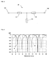
- Fig. 1 is a diagram of a filter circuit according to a first embodiment of the present invention
- Fig. 2 is a graph showing frequency characteristics of the filter circuit according to the first embodiment of the present invention.
- Fig. 3 is a diagram of a filter circuit as a reference example for comparison with the present invention.
- Fig. 4 is a graph showing frequency characteristics of the filter circuit as a reference example for comparison with the present invention.
- Fig. 5 is a diagram for explaining one example of a theoretical analysis in the first embodiment of the present invention.
- Fig. 6 is a diagram for explaining an even-mode equivalent circuit in one example of the theoretical analysis in the first embodiment of the present invention.
- Fig. 7 is a diagram for explaining an odd-mode equivalent circuit in one example of the theoretical analysis in the first embodiment of the present invention.
- Fig. 8 is a graph showing frequency characteristics of Example 1 in the first embodiment
- Fig. 9 is a graph showing frequency characteristics of Example 2 in the first embodiment
- Fig. 10 is a graph showing frequency characteristics of another Example in the first embodiment
- Fig. 11 is a graph showing frequency characteristics of still another Example in the first embodiment
- Fig. 12 is a diagram of a filter circuit according to a second embodiment of the present invention.
- Fig. 13 is a graph showing frequency characteristics of the filter circuit according to the second embodiment of the present invention.
- Fig. 14 is a diagram of a filter circuit according to a third embodiment of the present invention.
- Fig. 15 is a graph showing frequency characteristics of the filter circuit according to the third embodiment of the present invention.
- Fig. 16 is a diagram of a filter circuit according to a fourth embodiment of the present invention.
- Fig. 17 is a graph showing frequency characteristics of the filter circuit according to the fourth embodiment of the present invention.
- Fig. 18 illustrates one modification of a distributed constant resonance circuit in the present invention
- Fig. 19 illustrates another modification of the distributed constant resonance circuit in the present invention
- Fig. 20 illustrates still another modification of the distributed constant resonance circuit in the present invention
- Fig. 21 illustrates still another modification of the distributed constant resonance circuit in the present invention
- Fig. 22 illustrates another modification of the distributed constant resonance circuit in the present invention
- Fig. 23 is a diagram of a filter circuit according to a fifth embodiment of the present invention.
- Fig. 24 is a graph showing frequency characteristics of the filter circuit according to the fifth embodiment of the present invention.
- Fig. 25 is a diagram of a filter circuit according to a sixth embodiment of the present invention.
- Fig. 26 is a graph showing frequency characteristics of the filter circuit according to the sixth embodiment of the present invention.
- Fig. 27 is a diagram of a filter circuit according to a seventh embodiment of the present invention.
- Fig. 28 is a graph showing frequency characteristics of the filter circuit according to the seventh embodiment of the present invention.
- Fig. 29 is a diagram of a filter circuit according to an eighth embodiment of the present invention.
- Fig. 30 is a graph showing frequency characteristics of the filter circuit according to the eighth embodiment of the present invention.
- Fig. 31 is a diagram of a filter circuit according to a ninth embodiment of the present invention.
- Fig. 32 is a graph showing frequency characteristics of the filter circuit according to the ninth embodiment of the present invention.
- Fig. 33 is a diagram of a band pass filter according to a tenth embodiment of the present invention.
- Fig. 34 is a graph showing frequency characteristics of the band pass filter according to the tenth embodiment of the present invention.
- Fig. 35 is a diagram of a band pass filter according to an eleventh embodiment of the present invention.
- Fig. 36 is a graph showing frequency characteristics of the band pass filter according to the eleventh embodiment of the present invention.
- Fig. 37 is a perspective view showing an external appearance of a filter circuit device according to a twelfth embodiment of the present invention.
- Fig. 38 is an explanatory view for explaining shapes and layout of conductor patterns of the filter circuit device according to the twelfth embodiment of the present invention.
- Fig. 39 is an explanatory view for explaining shapes and layout of the conductor patterns of the filter circuit device according to the twelfth embodiment of the present invention.
- Fig. 40 is an explanatory view for explaining shapes and layout of conductor patterns of the filter circuit device according to the twelfth embodiment of the present invention.
- Fig. 41 is a diagram showing an equivalent circuit of the filter circuit device according to the twelfth embodiment of the present invention.
- Fig. 42 is a graph showing frequency characteristics of the filter circuit device according to the twelfth embodiment of the present invention.
- Fig. 43 is a side view showing, in a seeing-through way, a high-frequency wireless circuit module according to a thirteenth embodiment of the present invention.
- Fig. 44 is a block diagram showing an electric circuit of the high-frequency wireless circuit module according to the thirteenth embodiment of the present invention.
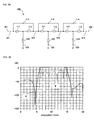
- FIG. 1 shows a filter circuit according to a first embodiment of the present invention.
- a filter circuit 100 according to the first embodiment shown in Fig. 1 which represents a filter circuit of the present invention, comprises a first impedance element 111 having an input end connected to an input terminal 101, a second impedance element 112 having an input end connected to an output end of the first impedance element 111 and an output end connected to an output terminal 102 and made of the same component as that of the first impedance element 111, a distributed constant resonance circuit 113 having one end connected to a junction between the output end of the first impedance element 111 and the input end of the second impedance element 112, and a third impedance element 114 having one end connected to the input end of the first impedance element 111 and the other end connected to the output end of the second impedance element 112.
- the first impedance element 111 and the second impedance element 112 are each made of a distributed constant resonance circuit constituted by a transmission line which has a predetermined distributed constant.
- the distributed constant resonance circuit 113 is made of an open stub type resonance circuit constituted by a transmission line which has a predetermined distributed constant and is opened at the other end of the distributed constant resonance circuit 113.
- the third impedance element 114 is made of a capacitor having a predetermined concentrated constant.
- the filter circuit 100 is a band-pass type filter circuit in which a wide band is realized by cancelling periodic attenuation poles that are in principle specific to the distributed-constant stub type resonance circuit serving as the distributed constant resonance circuit 113, and it has a very simple structure comprising one distributed-constant stub type resonance circuit, two transmission lines (i.e., very short transmission lines of about 1/10 wavelength), and one capacitor.
- the open stub type resonance circuit serving as the distributed constant resonance circuit 113 is set such that an electrical length is 180° and a characteristic impedance is 40 ⁇ at the resonance frequency of 6 GHz.
- Fig. 3 shows a filter circuit as a reference example for comparison with the present invention.
- a filter circuit 10 as the reference example has a structure that the third impedance element 114 is removed from the filter circuit 100.
- a distributed constant filter such as a laminated filter, like the filter circuit 10 shown in Fig. 3 , is mainly constituted by a method using, as a basis, a stub type resonance circuit with a 1/4 or 1/2 wavelength.
- the horizontal axis represents frequency
- the vertical axis represents amounts of attenuation and reflection.
- a characteristic curve A and a characteristic curve B in Fig. 4 represent a band pass characteristic and a reflection characteristic, respectively.
- the distributed-constant stub type resonance circuit serving as the distributed constant resonance circuit 113 in the filter circuit 10 of Fig. 3 has such a characteristic that an electrical length is 180° and a characteristic impedance is 40 ⁇ at the frequency of 6 GHz.
- Fig. 2 shows a characteristic example of the filter circuit 100 according to the first embodiment.
- the horizontal axis represents frequency
- the vertical axis represents amounts of attenuation and reflection.
- a characteristic curve A and a characteristic curve B in Fig. 2 represent a band pass characteristic and a reflection characteristic, respectively.
- the attenuation pole at 9 GHz among the periodic attenuation poles specific to the stub type resonance circuit disappears. It is also seen that the number of matching frequencies is increased to three. Stated another way, the filter circuit 100 can cancel the attenuation pole that is in principle specific to the distributed-constant stub type resonance circuit, and can widen a passband of the distributed-constant stub type resonance circuit by increasing the number of matching frequencies.
- Conditions for generation of the attenuation pole can be easily determined by a theoretical analysis, and the position, etc. of the attenuation pole in the frequency characteristics of the filter circuit 100 can be adjusted by setting the constants of the impedance elements, etc. so as to satisfy the conditions.
- each of the transmission lines forming the first impedance element 111 and the second impedance element 112 has a characteristic impedance Z 2 and an electrical length ⁇ 2
- the distributed constant resonance circuit 113 is made of a 1/2-wavelength open stub and has a characteristic impedance Z 1 and an electrical length ⁇ 1
- the fourth impedance element 114 is made of a capacitor with a capacitance C 1 .
- a characteristic impedance in each of the input terminal side and the output terminal side is Z 0 .
- Figs. 1 and 5 have a bilaterally symmetric circuit configuration, an even-odd mode analysis can be performed.
- Fig. 6 shows an even-mode equivalent circuit
- Fig. 7 shows an odd-mode equivalent circuit.
- the even-mode equivalent circuit shown in Fig. 6 , comprises a transmission line TL1 having one end connected to a terminal Port1, and a 1/2-wavelength open stub OES connected to the other end of the transmission line TL1.
- the terminal Port1 has a characteristic impedance Z 0
- the transmission line TL1 has a characteristic impedance Z 2 and an electrical length ⁇ 2
- the open stub OES has a characteristic impedance 2Z 1 and an electrical length ⁇ 1 .
- the odd-mode equivalent circuit shown in Fig. 7 , comprises a transmission line TL2 having one end connected to the terminal Port1 and the other end grounded, and a capacitor CP having one end connected to the terminal Port1 and the other end grounded.
- the terminal Port1 has the characteristic impedance Z 0
- the transmission line TL2 has a characteristic impedance Z 2 and an electrical length ⁇ 2
- the capacitor CP has a capacitance 2C 1 .
- an input impedance Z even and a reflection coefficient ⁇ even in the even mode are expressed by the following formulae (1) and (2), respectively:
- Z even j ⁇ Z 2 ⁇ Z 2 ⁇ tan ⁇ 1 tan ⁇ 2 - 2 ⁇ Z 1 Z 2 ⁇ tan ⁇ 1 + 2 ⁇ Z 1 tan ⁇ 2
- an input impedance Z odd and a reflection coefficient ⁇ odd in the odd mode are expressed by the following formulae (3) and (4), respectively:
- Z odd 1 2 ⁇ j ⁇ ⁇ C 1 + 1 j ⁇ Z 2 tan ⁇ 2
- the attenuation pole frequency and the matching frequency in each of those circuits can also be determined by executing the theoretical analysis in the even and odd modes as described above.
- Fig. 8 shows frequency characteristics of Example 1.
- the horizontal axis represents frequency
- the vertical axis represents amounts of attenuation and reflection.
- a characteristic curve A and a characteristic curve B in Fig. 8 represent a band pass characteristic and a reflection characteristic, respectively.
- each of the transmission lines constituting the first impedance element 111 and the second impedance element 112 has a characteristic impedance of 30 ⁇ and an electrical length of 18° at the frequency of 6 GHz.
- the transmission line constituting the distributed constant resonance circuit 113 has a characteristic impedance of 40 ⁇ and an electrical length of 180° at the frequency of 6 GHz.
- the capacitor constituting the third impedance element 114 has a capacitance of 0.68 pF.
- Fig. 9 shows frequency characteristics of Example 2.
- the horizontal axis represents frequency
- the vertical axis represents amounts of attenuation and reflection.
- a characteristic curve A and a characteristic curve B in Fig. 9 represent a band pass characteristic and a reflection characteristic, respectively.
- each of the transmission lines constituting the first impedance element 111 and the second impedance element 112 has a characteristic impedance of 32 ⁇ and an electrical length of 56° at the frequency of 6 GHz.
- the transmission line constituting the distributed constant resonance circuit 113 has a characteristic impedance of 40 ⁇ and an electrical length of 180° at the frequency of 6 GHz.
- the capacitor constituting the third impedance element 114 has a capacitance of 0.14 pF.
- the position of the attenuation pole in the lower frequency side i.e., the position of the attenuation pole at 3 GHz in the frequency characteristics of Figs. 8 and 9 , depends only on the length of the open stub type resonance circuit constituting the distributed constant resonance circuit 113.
- the attenuation pole in the higher frequency side i.e., the attenuation pole present in the higher frequency side than 8 GHz in the frequency characteristics of Figs. 8 and 9 , can be controlled by the transmission lines constituting the first impedance element 111 and the second impedance element 112 and the capacitor constituting the third impedance element 114.
- the attenuation pole in the higher frequency side is shifted toward the lower frequency side.
- the attenuation pole in the higher frequency side is shifted toward the even higher frequency side.
- two or more attenuation poles adjacent to each other can be produced in the higher frequency side.
- the position of the attenuation pole in the lower frequency side depends only on the length of the open stub type resonance circuit constituting the distributed constant resonance circuit 113.
- the number and positions of the attenuation poles in the higher frequency side depend on the characteristic impedance and the electrical length of each of the transmission lines constituting the first impedance element 111 and the second impedance element 112, the characteristic impedance of the open stub type resonance circuit constituting the distributed constant resonance circuit 113, and the capacitance of the capacitor constituting the third impedance element 114.
- Fig. 12 is a diagram of a filter circuit according to the second embodiment of the present invention
- Fig. 13 is a graph showing frequency characteristics of the filter circuit according to the second embodiment.
- the second embodiment will be described in connection with a filter circuit which is adapted for realizing a band pass filter having a wide frequency passband of 3 - 10 GHz.
- a filter circuit 100B shown in Fig. 12 comprises a first impedance element 111 having an input end connected to an input terminal 101, a second impedance element 112 having an input end connected to an output end of the first impedance element 111 and an output end connected to an output terminal 102 and made of the same component as that of the first impedance element 111, a distributed constant resonance circuit 113 having one end connected to a junction between the output end of the first impedance element 111 and the input end of the second impedance element 112, and a third impedance element 114 having one end connected to the input end of the first impedance element 111 and the other end connected to the output end of the second impedance element 112.
- the first impedance element 111 and the second impedance element 112 are each made of an inductor having a predetermined concentrated constant.
- the distributed constant resonance circuit 113 is made of an open stub type resonance circuit constituted by a transmission line which has a predetermined distributed constant and is opened at the other end of the distributed constant resonance circuit 113.
- the third impedance element 114 is made of a capacitor having a predetermined concentrated constant.
- the filter circuit 100B of the second embodiment is also a band-pass type filter circuit in which a wide band is realized by cancelling periodic attenuation poles that are in principle specific to the distributed-constant stub type resonance circuit serving as the distributed constant resonance circuit 113, and it has a very simple structure comprising one distributed-constant stub type resonance circuit, two inductors, and one capacitor.
- each of the inductors constituting the first and second impedance elements 111, 112 has an inductance of 0.35 nH.
- the transmission line constituting the distributed constant resonance circuit 113 has a characteristic impedance of 18 ⁇ and an electrical length of 18° at the frequency of 6 GHz.
- the capacitor constituting the third impedance element 114 has a capacitance of 0.54 pF.
- this second embodiment also realizes, as shown in Fig. 13 , the band-pass type filter circuit having a wide frequency passband of 3 - 10 GHz.
- conditions for generation of the attenuation pole can be easily determined by a theoretical analysis, and the position, etc. of the attenuation pole in the frequency characteristics of the filter circuit 100B can be adjusted by setting the constants of the impedance elements, etc. so as to satisfy the conditions.
- Fig. 14 is a diagram of a filter circuit according to the third embodiment of the present invention
- Fig. 15 is a graph showing frequency characteristics of the filter circuit according to the third embodiment.
- the third embodiment will be described in connection with a filter circuit which is adapted for realizing a band pass filter having a wide frequency passband of 3 - 10 GHz.
- a filter circuit 100C shown in Fig. 14 comprises a first impedance element 111 having an input end connected to an input terminal 101, a second impedance element 112 having an input end connected to an output end of the first impedance element 111 and an output end connected to an output terminal 102 and made of the same component as that of the first impedance element 111, a distributed constant resonance circuit 113 having one end connected to a junction between the output end of the first impedance element 111 and the input end of the second impedance element 112, and a third impedance element 114 having one end connected to the input end of the first impedance element 111 and the other end connected to the output end of the second impedance element 112.
- the first impedance element 111 and the second impedance element 112 are each made of a capacitor having a predetermined concentrated constant.
- the distributed constant resonance circuit 113 is made of an open stub type resonance circuit constituted by a transmission line which has a predetermined distributed constant and is opened at the other end of the distributed constant resonance circuit 113.
- the third impedance element 114 is made of a transmission line having a predetermined distributed constant.
- the filter circuit 100C of the third embodiment is also a band-pass type filter circuit in which a wide band is realized by cancelling periodic attenuation poles that are in principle specific to the distributed-constant stub type resonance circuit serving as the distributed constant resonance circuit 113, and it has a very simple structure comprising one distributed-constant stub type resonance circuit, two capacitors, and one distributed-constant type transmission line.
- each of the capacitors constituting the first and second impedance elements 111, 112 has a capacitance of 1.14 pF.
- the transmission line constituting the distributed constant resonance circuit 113 has a characteristic impedance of 32.5 ⁇ and an electrical length of 180° at the frequency of 6 GHz.
- the transmission line constituting the third impedance element 114 has a characteristic impedance of 30 ⁇ and an electrical length of 36° at the frequency of 6 GHz.
- this third embodiment also realizes, as shown in Fig. 15 , the band-pass type filter circuit having a wide frequency passband of 3 - 10 GHz.
- conditions for generation of the attenuation pole can be easily determined by a theoretical analysis, and the position, etc. of the attenuation pole in the frequency characteristics of the filter circuit 100C can be adjusted by setting the constants of the impedance elements, etc. so as to satisfy the conditions.
- Fig. 16 is a diagram of a filter circuit according to the fourth embodiment of the present invention
- Fig. 17 is a graph showing frequency characteristics of the filter circuit according to the fourth embodiment.
- the fourth embodiment will be described in connection with a filter circuit which is adapted for realizing a band pass filter having a wide frequency passband of 4 - 14 GHz.
- a filter circuit 100D shown in Fig. 16 comprises a first impedance element 111 having an input end connected to an input terminal 101, a second impedance element 112 having an input end connected to an output end of the first impedance element 111 and an output end connected to an output terminal 102 and made of the same component as that of the first impedance element 111, a distributed constant resonance circuit 113 having one end connected to a junction between the output end of the first impedance element 111 and the input end of the second impedance element 112, and a third impedance element 114 having one end connected to the input end of the first impedance element 111 and the other end connected to the output end of the second impedance element 112.
- the first impedance element 111 and the second impedance element 112 are each made of a capacitor having a predetermined concentrated constant.
- the distributed constant resonance circuit 113 is made of an open stub type resonance circuit constituted by a transmission line which has a predetermined distributed constant and is opened at the other end of the distributed constant resonance circuit 113.
- the third impedance element 114 is made of an inductor having a predetermined concentrated constant.
- the filter circuit 100D of the fourth embodiment is also a band-pass type filter circuit in which a wide band is realized by cancelling periodic attenuation poles that are in principle specific to the distributed-constant stub type resonance circuit serving as the distributed constant resonance circuit 113, and it has a very simple structure comprising one distributed-constant stub type resonance circuit, two capacitors, and one inductor.
- each of the capacitors constituting the first and second impedance elements 111, 112 has a capacitance of 1.416 pF.
- the transmission line constituting the distributed constant resonance circuit 113 has a characteristic impedance of 35.2 ⁇ and an electrical length of 180° at the frequency of 6 GHz.
- the inductor constituting the third impedance element 114 has an inductance of 0.42 nH.
- this fourth embodiment realizes, as shown in Fig. 17 , the band-pass type filter circuit having a wide frequency passband of 4 - 14 GHz.
- conditions for generation of the attenuation pole can be easily determined by a theoretical analysis, and the position, etc. of the attenuation pole in the frequency characteristics of the filter circuit 100D can be adjusted by setting the constants of the impedance elements, etc. so as to satisfy the conditions.
- the distributed constant resonance circuit 113 can be constituted, for example, as shown in Figs. 18-22 .
- the distributed constant resonance circuit 113 is made of a short stub type resonance circuit constituted by a transmission line 121 which has a predetermined distributed constant and is grounded at the other end thereof.
- the distributed constant resonance circuit 113 is made of a transmission line 122 which has a predetermined distributed constant and is grounded at the other end thereof through a capacitor 123.
- Fig. 18 the distributed constant resonance circuit 113 is made of a short stub type resonance circuit constituted by a transmission line 121 which has a predetermined distributed constant and is grounded at the other end thereof.
- the distributed constant resonance circuit 113 is made of a transmission line 122 which has a predetermined distributed constant and is grounded at the other end thereof through a capacitor 123.
- the distributed constant resonance circuit 113 is made of a transmission line 125 which has a predetermined distributed constant and which is connected at one end thereof to a capacitor 124 and is grounded at the other end thereof.
- the distributed constant resonance circuit 113 is constituted by interconnecting respective one ends of two transmission lines 126 and 127, each of which has a predetermined distributed constant and is opened at the other end thereof.
- the distributed constant resonance circuit 113 is constituted by interconnecting respective one ends of two transmission lines (distributed constant resonance circuits) 128 and 129, each of which has a predetermined distributed constant and is grounded at the other end thereof.
- a fifth embodiment of the present invention will be described below in relation to the case where the transmission line 121 shown in Fig. 18 is employed as the distributed constant resonance circuit 113.
- Fig. 23 is a diagram of a filter circuit according to the fifth embodiment of the present invention
- Fig. 24 is a graph showing frequency characteristics of the filter circuit according to the fifth embodiment.
- the fifth embodiment will be described in connection with a filter circuit which is adapted for realizing a band pass filter having a wide frequency passband of 3 - 10 GHz.
- a filter circuit 100E shown in Fig. 23 comprises a first impedance element 111 having an input end connected to an input terminal 101, a second impedance element 112 having an input end connected to an output end of the first impedance element 111 and an output end connected to an output terminal 102 and made of the same component as that of the first impedance element 111, a distributed constant resonance circuit 121 having one end connected to a junction between the output end of the first impedance element 111 and the input end of the second impedance element 112, and a third impedance element 114 having one end connected to the input end of the first impedance element 111 and the other end connected to the output end of the second impedance element 112.
- the first impedance element 111 and the second impedance element 112 are each made of a distributed constant resonance circuit constituted by a transmission line which has a predetermined distributed constant.
- the distributed constant resonance circuit 121 is made of a short stub type resonance circuit constituted by a transmission line which has a predetermined distributed constant and is grounded at the other end of the distributed constant resonance circuit 121.
- the third impedance element 114 is made of a capacitor having a predetermined concentrated constant.
- the filter circuit 100E of the fifth embodiment is also a band-pass type filter circuit realizing a wide band, and it has a very simple structure comprising one distributed-constant stub type resonance circuit, two transmission lines, and one capacitor.
- each of the transmission lines (distributed constant resonance circuits) constituting the first and second impedance elements 111, 112 has a characteristic impedance of 50 ⁇ and an electrical length of 180° at the frequency of 6 GHz.
- the transmission line constituting the distributed constant resonance circuit 121 has a characteristic impedance of 50 ⁇ and an electrical length of 20° at the frequency of 6 GHz.
- the capacitor constituting the third impedance element 114 has a capacitance of 0.85 pF.
- this fifth embodiment also realizes, as shown in Fig. 24 , the band-pass type filter circuit having a wide frequency passband of 3 - 10 GHz.
- conditions for generation of the attenuation pole can be easily determined by a theoretical analysis, and the position, etc. of the attenuation pole in the frequency characteristics of the filter circuit 100E can be adjusted by setting the constants of the impedance elements, etc. so as to satisfy the conditions.
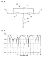
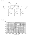
- a sixth embodiment of the present invention will be described below in relation to the case where the transmission line 122 and the capacitor 123, shown in Fig. 19 , are employed as the distributed constant resonance circuit 113.
- Fig. 25 is a diagram of a filter circuit according to the sixth embodiment of the present invention
- Fig. 26 is a graph showing frequency characteristics of the filter circuit according to the sixth embodiment.
- the sixth embodiment will be described in connection with a filter circuit which is adapted for realizing a band pass filter having a wide frequency passband of 7 - 13 GHz.
- a filter circuit 100F shown in Fig. 25 comprises a first impedance element 111 having an input end connected to an input terminal 101, a second impedance element 112 having an input end connected to an output end of the first impedance element 111 and an output end connected to an output terminal 102 and made of the same component as that of the first impedance element 111, a transmission line 122 having one end connected to a junction between the output end of the first impedance element 111 and the input end of the second impedance element 112, a capacitor 123 having one end connected to the other end of the transmission line 122 and the other end grounded, and a third impedance element 114 having one end connected to the input end of the first impedance element 111 and the other end connected to the output end of the second impedance element 112.
- the first impedance element 111 and the second impedance element 112 are each made of a distributed constant resonance circuit constituted by a transmission line which has a predetermined distributed constant.
- the third impedance element 114 is made of a capacitor having a predetermined concentrated constant.
- the filter circuit 100F of the sixth embodiment is also a band-pass type filter circuit realizing a wide band, and it has a very simple structure comprising one distributed-constant stub type resonance circuit, two transmission lines, and two capacitors.
- each of the transmission lines (distributed constant resonance circuits) constituting the first and second impedance elements 111, 112 has a characteristic impedance of 35 ⁇ and an electrical length of 18° at the frequency of 6 GHz.
- the transmission line 122 and the capacitor 123 both constituting the distributed constant resonance circuit 113 the transmission line 122 has a characteristic impedance of 50 ⁇ and an electrical length of 180° at the frequency of 6 GHz, and the capacitor 123 has a capacitance of 2 pF.
- the capacitor constituting the third impedance element 114 has a capacitance of 1.15 pF.
- this sixth embodiment realizes, as shown in Fig. 26 , the band-pass type filter circuit having a wide frequency passband of 7 - 13 GHz.
- conditions for generation of the attenuation pole can be easily determined by a theoretical analysis, and the position, etc. of the attenuation pole in the frequency characteristics of the filter circuit 100F can be adjusted by setting the constants of the impedance elements, etc. so as to satisfy the conditions.
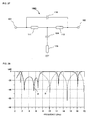
- a seventh embodiment of the present invention will be described below in relation to the case where the capacitor 124 and the transmission line 125, shown in Fig. 20 , are employed as the distributed constant resonance circuit 113.
- Fig. 27 is a diagram of a filter circuit according to the seventh embodiment of the present invention
- Fig. 28 is a graph showing frequency characteristics of the filter circuit according to the seventh embodiment.
- the seventh embodiment will be described in connection with a filter circuit which is adapted for realizing a band pass filter having a wide frequency passband of 7 - 12 GHz.
- a filter circuit 100G shown in Fig. 27 comprises a first impedance element 111 having an input end connected to an input terminal 101, a second impedance element 112 having an input end connected to an output end of the first impedance element 111 and an output end connected to an output terminal 102 and made of the same component as that of the first impedance element 111, a capacitor 124 having one end connected to a junction between the output end of the first impedance element 111 and the input end of the second impedance element 112, a transmission line 125 having one end connected to the other end of the capacitor 124 and the other end grounded, and a third impedance element 114 having one end connected to the input end of the first impedance element 111 and the other end connected to the output end of the second impedance element 112.
- the first impedance element 111 and the second impedance element 112 are each made of a distributed constant resonance circuit constituted by a transmission line which has a predetermined distributed constant.
- the third impedance element 114 is made of a capacitor having a predetermined concentrated constant.
- the filter circuit 100G of the seventh embodiment is also a band-pass type filter circuit realizing a wide band, and it has a very simple structure comprising one distributed-constant stub type resonance circuit, two transmission lines, and two capacitors.
- each of the transmission lines constituting the first and second impedance elements 111, 112 has a characteristic impedance of 37 ⁇ and an electrical length of 30° at the frequency of 6 GHz.
- the transmission line 125 and the capacitor 124 both constituting the distributed constant resonance circuit 113 the transmission line 125 has a characteristic impedance of 40 ⁇ and an electrical length of 180° at the frequency of 6 GHz, and the capacitor 124 has a capacitance of 2 pF.
- the capacitor constituting the third impedance element 114 has a capacitance of 0.65 pF.
- this seventh embodiment realizes, as shown in Fig. 28 , the band-pass type filter circuit having a wide frequency passband of 7 - 12 GHz.
- conditions for generation of the attenuation pole can be easily determined by a theoretical analysis, and the position, etc. of the attenuation pole in the frequency characteristics of the filter circuit 100G can be adjusted by setting the constants of the impedance elements, etc. so as to satisfy the conditions.
- Fig. 29 is a diagram of a filter circuit according to the eighth embodiment of the present invention
- Fig. 30 is a graph showing frequency characteristics of the filter circuit according to the eighth embodiment.
- the eighth embodiment will be described in connection with a filter circuit which is adapted for realizing a band pass filter having a wide frequency passband of 4 - 18 GHz.
- a filter circuit 100H shown in Fig. 29 comprises a first impedance element 111 having an input end connected to an input terminal 101, a second impedance element 112 having an input end connected to an output end of the first impedance element 111 and an output end connected to an output terminal 102 and made of the same component as that of the first impedance element 111, two transmission lines 126 and 127 each of which has one end connected to a junction between the output end of the first impedance element 111 and the input end of the second impedance element 112 and has the other end being opened, and a third impedance element 114 having one end connected to the input end of the first impedance element 111 and the other end connected to the output end of the second impedance element 112.
- the first impedance element 111 and the second impedance element 112 are each made of a distributed constant resonance circuit constituted by a transmission line which has a predetermined distributed constant.
- the third impedance element 114 is made of a capacitor having a predetermined concentrated constant.
- the filter circuit 100H of the eighth embodiment is also a band-pass type filter circuit realizing a wide band, and it has a very simple structure comprising two distributed-constant stub type resonance circuits, two transmission lines, and one capacitor.
- each of the transmission lines constituting the first and second impedance elements 111, 112 has a characteristic impedance of 45 ⁇ and an electrical length L1 of 18° at the frequency of 2 GHz.
- the transmission line 126 and 127 constituting the distributed constant resonance circuit 113 the transmission line 126 has a characteristic impedance of 50 ⁇ and an electrical length L2 of 45° at the frequency of 2 GHz
- the capacitor constituting the third impedance element 114 has a capacitance of 1 pF.
- this sixth embodiment realizes, as shown in Fig. 30 , the band-pass type filter circuit having a wide frequency passband of 4 - 18 GHz.
- conditions for generation of the attenuation pole can be easily determined by a theoretical analysis, and the position, etc. of the attenuation pole in the frequency characteristics of the filter circuit 100H can be adjusted by setting the constants of the impedance elements, etc. so as to satisfy the conditions.
- a ninth embodiment of the present invention will be described below in relation to the case where the transmission lines 128 and 129, shown in Fig. 22 , are employed as the distributed constant resonance circuit 113.
- Fig. 31 is a diagram of a filter circuit according to the ninth embodiment of the present invention
- Fig. 32 is a graph showing frequency characteristics of the filter circuit according to the ninth embodiment.
- the ninth embodiment will be described in connection with a filter circuit which is adapted for realizing a band pass filter having a wide frequency passband of 1 - 13 GHz.
- a filter circuit 100I shown in Fig. 31 comprises a first impedance element 111 having an input end connected to an input terminal 101, a second impedance element 112 having an input end connected to an output end of the first impedance element 111 and an output end connected to an output terminal 102 and made of the same component as that of the first impedance element 111, two transmission lines 128 and 129 each of which has one end connected to a junction between the output end of the first impedance element 111 and the input end of the second impedance element 112 and has the other end being grounded, and a third impedance element 114 having one end connected to the input end of the first impedance element 111 and the other end connected to the output end of the second impedance element 112.
- the first impedance element 111 and the second impedance element 112 are each made of a distributed constant resonance circuit constituted by a transmission line which has a predetermined distributed constant.
- the third impedance element 114 is made of a capacitor having a predetermined concentrated constant.
- the filter circuit 100I of the ninth embodiment is also a band-pass type filter circuit realizing a wide band, and it has a very simple structure comprising two distributed-constant stub type resonance circuits, two transmission lines, and one capacitor.
- each of the transmission lines constituting the first and second impedance elements 111, 112 has a characteristic impedance of 45 ⁇ and an electrical length L1 of 18° at the resonance frequency of 6 GHz.
- the transmission line 128 and 129 constituting the distributed constant resonance circuit 113 the transmission line 128 has a characteristic impedance of 30 ⁇ and an electrical length L2 of 45° at the frequency of 6 GHz
- the capacitor constituting the third impedance element 114 has a capacitance of 0.6 pF.
- this ninth embodiment realizes, as shown in Fig. 32 , the band-pass type filter circuit having a wide frequency passband of 1 - 13 GHz.
- conditions for generation of the attenuation pole can be easily determined by a theoretical analysis, and the position, etc. of the attenuation pole in the frequency characteristics of the filter circuit 100I can be adjusted by setting the constants of the impedance elements, etc. so as to satisfy the conditions.
- the filter circuits according to the foregoing embodiments are very useful filter circuits which can realize an "ultra wide band characteristic", a “multiple attenuation-pole characteristic”, and a “harmonic resonance suppression characteristic" by proper setting of the element values.
- a BPF Band Pass Filter
- a BPF 300 is constituted by connecting two sets of filter circuits 100F between an input terminal 301 and an output terminal 302 in series with capacitors 311-313 interposed as shown.
- Fig. 34 shows frequency characteristics of the BPF 300.
- a curve A represents an attenuation characteristic curve
- a curve B represents a reflection characteristic curve.
- the vertical axis represents amounts [dB] of attenuation and reflection
- the horizontal axis represents frequency [GHz].
- the attenuation characteristic curve A the amount of attenuation is maximized at 4.8 GHz and 17.5 GHz.
- the reflection characteristic curve B the amount of reflection is minimized at 6.7 GHz, 8.6 GHz, 12.0 GHz and 14.3 GHz.
- the filter circuit 300 is designed to have a passband of 6 - 10 GHz.
- a BPF 400 is constituted by connecting three sets of filter circuits 100F between an input terminal 401 and an output terminal 402 in series with capacitors 411-414 interposed as shown.
- Fig. 36 shows frequency characteristics of the BPF 400.
- a curve A represents an attenuation characteristic curve
- a curve B represents a reflection characteristic curve.
- the vertical axis represents amounts [dB] of attenuation and reflection
- the horizontal axis represents frequency [GHz].
- the attenuation characteristic curve A the amount of attenuation is maximized at 4.5 GHz, 5.0 GHz, 16.5 GHz and 20.0 GHz.
- the reflection characteristic curve B the amount of reflection is minimized at 6.3 GHz, 7.0 GHz, 9.0 GHz, 11.8 GHz, 13.8 GHz and 14.8 GHz.
- the filter circuit 400 is designed to have a passband of 6 - 15 GHz.
- a BPF having superior frequency characteristics can be constituted by connecting two or more sets of the above-described filter circuits 100 - 100I in series with capacitors interposed therebetween.
- a filter circuit, a diplexer circuit, etc. realizing desired characteristics and shapes can be obtained by changing combinations of the above-described filter circuits and connections between them.
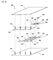
- Fig. 37 shows, as a twelfth embodiment, an external appearance of a filter circuit device 530 that is obtained by forming the filter circuit 100 as one unit of device. More specifically, the filter circuit device 530 is constituted such that the filter circuit 100 is formed in a multilayered structure within a rectangular parallelepiped multilayered member 531 which is mainly made of a dielectric ceramic, and external terminal electrodes 532-535 are formed on an outer surface of the multilayered member 531.
- the external terminal electrode 532 corresponds to the input terminal 101
- the external terminal electrode 533 corresponds to the output terminal 102.
- the external terminal electrodes 534 and 535 are grounded terminals.
- Figs. 38-40 illustrate shapes and layouts of conductor patterns in the case where another example of a BPF employing the above-described filter circuit 100F is formed inside a multilayered circuit board.
- Fig. 38 is a layout view looking, from above, only conductor patterns of a filter circuit device having a modified circuit in which filter circuits are added to the upstream and downstream sides in the twelfth embodiment.
- Fig. 39 illustrates layout of electrodes and layout of via conductors 544 in a state resulting from adding a ceramic multilayered substrate to the conductor patters, shown in Fig. 38 , in a way seeing through the interior from the right side indicated by A-A ( Fig. 38 ) instead of viewing it taken along a cross-section.
- Fig. 40 is an exploded perspective view for explaining, in a disassembled form, positional relationships among only the conductor patterns shown in Fig. 38 .
- numeral 540 denotes a multilayered circuit board which is mainly made of a dielectric ceramic 540a and in which a plurality of conductor patterns are arranged in a multilayered structure to form a later-described filter circuit 590 shown in Fig. 41 (modification of Fig. 25 ). More specifically, in an area of the multilayered circuit board 540 where the filter circuit 590 is formed, grounded conductor patterns 541 and 542 parallel to each other are arranged respectively on a front surface and a rear surface. Other grounded conductor patterns 543 each having a predetermined size are disposed between and parallel to the grounded conductor patterns 541 and 542.
- the grounded conductor patterns 543 are connected to the grounded conductor patterns 541 and 542 for electrical conduction through a plurality of via conductors 544. Further, an input-side conductor pattern 550, an output-side conductor pattern 560, a resonance conductor pattern 570, and a connecting conductor pattern 580 are disposed between the grounded conductor patterns 541 and 542.
- the input-side conductor pattern 550 is disposed parallel to the grounded conductor patterns 541 and 542, and it constitutes a second main resonance portion comprising an input-side strip line 551, a capacitor electrode 552 connected to the input-side conductor pattern 550 and constituting a second capacitor portion, a strip line 553 having one end connected to the capacitor electrode 552, and a capacitor electrode 554 connected to the other end of the strip line 553.
- a capacitor electrode 554 is arranged to face the grounded conductor pattern 543.
- the output-side conductor pattern 560 is disposed parallel to the grounded conductor patterns 541 and 542 in the same plane as the input-side conductor pattern 550, and it constitutes a third main resonance portion comprising an output-side strip line 561, a capacitor electrode 562 connected to the output-side conductor pattern 560 and constituting a third capacitor portion, a strip line 563 having one end connected to the capacitor electrode 562 and arranged parallel to the strip line 553, and a capacitor electrode 564 connected to the other end of the strip line 563.
- the capacitor electrode 564 is arranged to face the grounded conductor pattern 543.
- the resonance conductor pattern 570 is disposed between the input-side conductor pattern 550 and the output-side conductor pattern 560 in the same plane as them, and it constitutes a first main resonance portion comprising a strip line 571 arranged parallel to the strip line 553 and a capacitor electrode 572 connected to the other end of the strip line 571.
- a capacitor electrode 572 is arranged to face the grounded conductor pattern 543.
- the connecting conductor pattern 580 is arranged in a layer differing from a layer in which the input-side conductor pattern 550, the output-side conductor pattern 560 and the resonance conductor pattern 570 are arranged, with the dielectric ceramic 540a interposed between those two layers.
- the connecting conductor pattern 580 comprises an integral conductor pattern and a capacitor electrode 587.
- the integral conductor patter is made up of a capacitor electrode 581 which is arranged to face the capacitor electrode 552 and constitutes the second capacitor portion, a capacitor electrode 585 which is arranged to face the capacitor electrode 562 and constitutes the third capacitor portion, a strip line 582 having one end connected to the capacitor electrode 581, a connecting electrode 583 connected to the other end of the strip line 582, a strip line 584 having one end connected to the connecting electrode 583 and the other end connected to the capacitor electrode 585, and a capacitor electrode 586 which is connected to the capacitor electrode 581 and constitutes the first capacitor portion.
- the capacitor electrode 587 has one open end arranged to face an open end of the capacitor electrode 586 with the dielectric ceramic 540a interposed between them and the other end connected to the capacitor electrode 585 through a via conductor 588, and it constitutes the first capacitor portion. Further, the connecting electrode 583 is connected to one end of the strip line 571 through a via conductor 573.
- Fig. 41 shows an equivalent circuit of the filter circuit device formed inside the multilayered circuit board 540.
- components of the equivalent circuit shown in Fig. 41 are constituted as follows.
- a transmission line 593 connected to an input terminal 591 is constituted by the strip line 553, a capacitor 597 is constituted by the capacitor electrode 552 and the capacitor electrode 581, and a transmission line 111 is constituted by the strip line 582.
- a transmission line 594 connected to an output terminal 592 is constituted by the strip line 563
- a capacitor 598 is constituted by the capacitor electrode 562 and the capacitor electrode 585
- a transmission line 112 is constituted by the strip line 584.
- the main resonance portion comprising a transmission line 122 and a capacitor 123 is constituted by the strip line 571, the capacitor electrode 572, and the grounded conductor pattern 543.
- a capacitor 114 connected between an input end of the input-side transmission line 111 and an output end of the output-side transmission line 112 is constituted by the capacitor electrode 586 and the capacitor electrode 587 arranged to face the former.
- a serial resonance circuit connected to the input terminal 591 and comprising the transmission line 593 and the capacitor 595 is constituted by the strip line 553, the capacitor electrode 554, and the grounded conductor patterns 543.
- a serial resonance circuit connected to the output terminal 592 and comprising the transmission line 594 and the capacitor 596 is constituted by the strip line 563, the capacitor electrode 564, and the grounded conductor patterns 543.
- Fig. 42 shows frequency characteristics of the filter circuit (band pass filter) 590 that is formed in the multilayered circuit board 540 as described above.
- a curve A represents an attenuation characteristic curve
- a curve B represents a reflection characteristic curve.
- the vertical axis represents amounts [dB] of attenuation and reflection
- the horizontal axis represents frequency [GHz].
- the attenuation characteristic curve A the amount of attenuation is maximized at 1.8 GHz, 5.2 GHz and 11.3 GHz.
- the reflection characteristic curve B the amount of reflection is minimized at 6.5 GHz, 7.0 GHz, 8.8 GHz and 10.5 GHz.
- the filter circuit 590 is designed to have a passband of 6 - 11 GHz on the basis of the above-described filter circuit 100F.
- the filter circuit device 530 shown in Fig. 37 can be constructed by removing the strip lines 551 and 553 and the capacitor electrode 554 of the input-side conductor pattern 550 and the strip lines 561 and 563 and the capacitor electrode 564 of the output-side conductor pattern 560, which are shown in Figs. 38-40 .
- the filter circuit of the present invention can be realized in a very small structure in the case using an LTCC (Low Temperature Co-fired Ceramics) substrate, an LTCC device, or the like in which a capacitor can be easily fabricated.
- LTCC Low Temperature Co-fired Ceramics
- a high-frequency wireless circuit module is constructed which includes a band pass filter (BPF) using the above-described filter circuit.
- BPF band pass filter
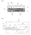
- Figs. 43 and 44 illustrate the thirteenth embodiment of the present invention. More specifically, Fig. 43 is a side view showing, in a seeing-through way, the high-frequency wireless circuit module according to the thirteenth embodiment of the present invention, and Fig. 44 is a block diagram showing an electric circuit of the high-frequency wireless circuit module according to the thirteenth embodiment of the present invention.
- numeral 600 denotes the high-frequency wireless circuit module in which electronic parts, such as an IC 621 and a passive element 622 both constituting a wireless transmit/receive function section (wireless function section), are mounted on a module substrate 601 that is made of a ceramic substrate, e.g., an LTCC (Low Temperature Co-fired Ceramics) substrate, or a resin substrate. Further, an upper surface of the module substrate 601 is covered with a shield member 602.
- the module substrate 601 includes therein conductor pattern electrodes 611 forming a band pass filter (BPF) 631, and conductor pattern electrodes 612 forming a balun 632.
- BPF band pass filter
- a circuit thus constituted can be connected to an external circuit through a plurality of external electrodes 641 which are formed on a bottom surface of the module substrate 601.
- the electric circuit of the high-frequency wireless circuit module 600 comprises the IC 621, the band pass filter (BPF) 631, and the balun 632.
- the input side of the band pass filter (BPF) 631 is connected to an external antenna 651 through the external electrode 641.
- the output side of the band pass filter (BPF) 631 is connected, inside the module substrate 601, to the input side of the balun 621, and the output side of the balun 621 is connected, inside the module substrate 601, to the IC 621 which constitutes the wireless transmit/receive function section (wireless function section).
- the band pass filter (BPF) 631 employing the filter circuit of the present invention can also be formed in a very small structure. Therefore, the high-frequency wireless circuit module 600 including the band pass filter (BPF) 631 can be obtained in a small size.
Landscapes
- Control Of Motors That Do Not Use Commutators (AREA)
- Filters And Equalizers (AREA)
Claims (11)
- Bandpassfilterschaltung, umfassend:ein in einer Eingangsseite angeordnetes erstes Impedanzelement (111);ein in einer Ausgangsseite angeordnetes zweites Impedanzelement (112) mit einem Eingangsende, das mit einem Ausgangsende des ersten Impedanzelements verbunden ist, und das aus derselben Komponente wie der des ersten Impedanzelements besteht;eine Resonanzschaltung (113) mit verteilter Konstante mit einem Ende, das mit einem Knoten zwischen dem Ausgangsende des ersten Impedanzelements und dem Eingangsende des zweiten Impedanzelements verbunden ist; undein drittes Impedanzelement (114) mit einem Ende, das mit dem Eingangsende des ersten Impedanzelements verbunden ist, und das andere Ende ist mit dem Ausgangsende des zweiten Impedanzelements verbunden,wobei mindestens eines des ersten bis dritten Impedanzelements durch ein Element dargestellt wird, das eine vorbestimmte konzentrierte Konstante aufweist, und die anderen Impedanzelemente jeweils durch ein Element dargestellt werden, das eine vorbestimmte verteilte Konstante aufweist.
- Bandpassfilterschaltung nach Anspruch 1, wobei das erste Impedanzelement und das zweite Impedanzelement jeweils aus einer Übertragungsleitung bestehen, die eine vorbestimmte verteilte Konstante aufweist,
wobei die Resonanzschaltung mit verteilter Konstante aus einer Resonanzschaltung des offenen Blindleitungstyps besteht, die durch eine Übertragungsleitung dargestellt wird, die eine vorbestimmte Verteilungskonstante aufweist und an dem anderen Ende der Resonanzschaltung mit verteilter Konstante geöffnet ist, und wobei das dritte Impedanzelement aus einem Kondensator besteht. - Bandpassfilterschaltung nach Anspruch 1, wobei das erste Impedanzelement und das zweite Impedanzelement jeweils aus einer Induktivität bestehen,
wobei die Resonanzschaltung mit verteilter Konstante aus einer Resonanzschaltung des offenen Blindleitungstyps besteht, die durch eine Übertragungsleitung dargestellt wird, die eine vorbestimmte Verteilungskonstante aufweist und an dem anderen Ende der Resonanzschaltung mit verteilter Konstante geöffnet ist, und
wobei das dritte Impedanzelement aus einem Kondensator besteht. - Bandpassfilterschaltung nach Anspruch 1, wobei das erste Impedanzelement und das zweite Impedanzelement jeweils aus einem Kondensator bestehen,
wobei die Resonanzschaltung mit verteilter Konstante aus einer Resonanzschaltung des offenen Blindleitungstyps besteht, die durch eine Übertragungsleitung dargestellt wird, die eine vorbestimmte Verteilungskonstante aufweist und an dem anderen Ende der Resonanzschaltung mit verteilter Konstante geöffnet ist, und
wobei das dritte Impedanzelement aus einer Übertragungsleitung besteht. - Bandpassfilterschaltung nach Anspruch 1, wobei das erste Impedanzelement und das zweite Impedanzelement jeweils aus einem Kondensator bestehen,
wobei die Resonanzschaltung mit verteilter Konstante aus einer Resonanzschaltung des offenen Blindleitungstyps besteht, die durch eine Übertragungsleitung dargestellt wird, die eine vorbestimmte Verteilungskonstante aufweist und an dem anderen Ende der Resonanzschaltung mit verteilter Konstante geöffnet ist, und
wobei das dritte Impedanzelement aus einer Induktivität besteht. - Bandpassfilterschaltung nach Anspruch 1, wobei die Resonanzschaltung mit verteilter Konstante aus einer oder mehreren Resonanzschaltungen des offenen Blindleitungstyps besteht, die jeweils durch eine Übertragungsleitung dargestellt werden, die eine vorbestimmte Verteilungskonstante aufweist und an dem anderen Ende der Resonanzschaltung mit verteilter Konstante geöffnet ist.
- Bandpassfilterschaltung nach Anspruch 1, wobei die Resonanzschaltung mit verteilter Konstante aus einer oder mehreren Resonanzschaltungen des kurzen Blindleitungstyps besteht, die jeweils durch eine Übertragungsleitung dargestellt werden, die eine vorbestimmte Verteilungskonstante aufweist und an dem anderen Ende der Resonanzschaltung mit verteilter Konstante mit Masse verbunden ist.
- Bandpassfilterschaltung nach Anspruch 1, wobei die Resonanzschaltung mit verteilter Konstante durch eine serielle Verbindung einer Resonanzschaltung des Blindleitungstyps dargestellt wird, die durch eine Übertragungsleitung, die eine vorbestimmte Verteilungskonstante aufweist, und einen Kondensator dargestellt wird.
- Bandpassfilterschaltungseinrichtung, wobei die Bandpassfilterschaltung nach einem der Ansprüche 1 bis 8 in einem Einrichtungsglied, das einen Einrichtungskörper darstellt, gebildet ist.
- Mehrschichtige Leiterplatte, in der die Bandpassfilterschaltung nach einem der Ansprüche 1 bis 8 gebildet ist.
- Schaltungsmodul, in dem die Bandpassfilterschaltung nach einem der Ansprüche 1 bis 8 gebildet ist.
Applications Claiming Priority (3)
| Application Number | Priority Date | Filing Date | Title |
|---|---|---|---|
| JP2007165298 | 2007-06-22 | ||
| JP2007333601 | 2007-12-26 | ||
| JP2008106440A JP4550915B2 (ja) | 2007-06-22 | 2008-04-16 | フィルタ回路及びフィルタ回路素子、これを備えた多層回路基板並びに回路モジュール |
Publications (3)
| Publication Number | Publication Date |
|---|---|
| EP2007012A2 EP2007012A2 (de) | 2008-12-24 |
| EP2007012A3 EP2007012A3 (de) | 2010-03-31 |
| EP2007012B1 true EP2007012B1 (de) | 2011-12-28 |
Family
ID=39816880
Family Applications (1)
| Application Number | Title | Priority Date | Filing Date |
|---|---|---|---|
| EP08252146A Not-in-force EP2007012B1 (de) | 2007-06-22 | 2008-06-20 | Filterschaltung, Filterschaltungsvorrichtung, mehrschichtige Leiterplatte und Schaltungsmodul, alle mit der Filterschaltung |
Country Status (2)
| Country | Link |
|---|---|
| US (1) | US20090027141A1 (de) |
| EP (1) | EP2007012B1 (de) |
Families Citing this family (15)
| Publication number | Priority date | Publication date | Assignee | Title |
|---|---|---|---|---|
| JP5757397B2 (ja) * | 2010-03-29 | 2015-07-29 | 株式会社ニコン | 露光方法及び露光装置、並びにデバイス製造方法 |
| JP2012191521A (ja) | 2011-03-11 | 2012-10-04 | Fujitsu Ltd | 可変フィルタ装置および通信装置 |
| US9438200B2 (en) * | 2014-03-26 | 2016-09-06 | Teledyne Wireless, Llc | Compact broadband impedance transformer |
| US10425480B2 (en) * | 2014-06-26 | 2019-09-24 | Hitachi Vantara Corporation | Service plan tiering, protection, and rehydration strategies |
| CN105141274B (zh) * | 2015-09-24 | 2018-08-07 | 重庆大及电子科技有限公司 | 滤波组件及其应用 |
| CN109075771B (zh) * | 2016-04-08 | 2022-08-16 | 谐振公司 | 射频滤波器,高选择性三工器和通信设备 |
| US10700666B2 (en) * | 2017-02-08 | 2020-06-30 | Taiyo Yuden Co., Ltd. | Filter circuit, multiplexer, and module |
| WO2020132011A1 (en) | 2018-12-20 | 2020-06-25 | Avx Corporation | High frequency multilayer filter |
| WO2020132183A1 (en) * | 2018-12-20 | 2020-06-25 | Avx Corporation | Multilayer electronic device including a capacitor having a precisely controlled capacitive area |
| US11509276B2 (en) | 2018-12-20 | 2022-11-22 | KYOCERA AVX Components Corporation | Multilayer filter including a return signal reducing protrusion |
| CN113273029B (zh) * | 2018-12-20 | 2022-08-02 | 京瓷Avx元器件公司 | 包括电容器的多层滤波器和形成多层滤波器的方法 |
| US11201602B1 (en) | 2020-09-17 | 2021-12-14 | Analog Devices, Inc. | Apparatus and methods for tunable filtering |
| EP3975330B1 (de) * | 2020-09-28 | 2025-01-22 | Nokia Technologies Oy | Funkkommunikation |
| US11201600B1 (en) | 2020-10-05 | 2021-12-14 | Analog Devices, Inc. | Apparatus and methods for control and calibration of tunable filters |
| CN116114179A (zh) * | 2020-10-12 | 2023-05-12 | 株式会社村田制作所 | 元件安装基板以及调整方法 |
Family Cites Families (19)
| Publication number | Priority date | Publication date | Assignee | Title |
|---|---|---|---|---|
| US2177761A (en) * | 1938-09-15 | 1939-10-31 | Hazeltine Corp | M-derived band-pass filter |
| JPS58190113A (ja) * | 1982-04-30 | 1983-11-07 | Fujitsu Ltd | 遅延等化器 |
| JPH04207706A (ja) * | 1990-11-30 | 1992-07-29 | Mitsubishi Electric Corp | フィルタ回路 |
| JPH04225601A (ja) * | 1990-12-27 | 1992-08-14 | Sharp Corp | 帯域除去フィルタ回路 |
| US5187457A (en) * | 1991-09-12 | 1993-02-16 | Eni Div. Of Astec America, Inc. | Harmonic and subharmonic filter |
| JPH06224644A (ja) * | 1993-01-25 | 1994-08-12 | Nec Corp | 半導体装置 |
| JPH11243306A (ja) * | 1998-02-25 | 1999-09-07 | Murata Mfg Co Ltd | 高周波モジュールおよびそれを用いた通信装置 |
| JP2000236201A (ja) * | 1999-02-16 | 2000-08-29 | Fujitsu Ltd | スプリアス低減回路 |
| US6621370B1 (en) * | 2000-09-15 | 2003-09-16 | Atheros Communications, Inc. | Method and system for a lumped-distributed balun |
| JP2005136836A (ja) * | 2003-10-31 | 2005-05-26 | Seiko Epson Corp | 逓倍発振回路及びこれを使用した無線通信装置 |
| JP4155576B2 (ja) | 2004-04-01 | 2008-09-24 | 国立大学法人東京工業大学 | リングフィルタ及びそれを用いた広帯域の帯域通過フィルタ |
| JP4250718B2 (ja) | 2004-04-30 | 2009-04-08 | 富士通コンポーネント株式会社 | フィルタ装置及び回路モジュール |
| JP4658644B2 (ja) * | 2005-03-10 | 2011-03-23 | 双信電機株式会社 | 遅延線 |
| JP2008115079A (ja) * | 2005-03-11 | 2008-05-22 | Mitsui Norin Co Ltd | 抗炎症剤 |
| JP4565145B2 (ja) | 2005-09-02 | 2010-10-20 | 独立行政法人情報通信研究機構 | 超広帯域バンドパスフィルタ |
| US20070120627A1 (en) * | 2005-11-28 | 2007-05-31 | Kundu Arun C | Bandpass filter with multiple attenuation poles |
| JP5016219B2 (ja) * | 2005-12-27 | 2012-09-05 | 太陽誘電株式会社 | 共振回路、フィルタ回路、及び多層基板 |
| US7535321B1 (en) * | 2006-01-17 | 2009-05-19 | Xilinx, Inc. | Method and apparatus for a printed circuit board (PCB) embedded filter |
| US7671706B2 (en) * | 2006-04-14 | 2010-03-02 | Murata Manufacturing Co., Ltd | High frequency multilayer bandpass filter |
-
2008
- 2008-06-18 US US12/141,870 patent/US20090027141A1/en not_active Abandoned
- 2008-06-20 EP EP08252146A patent/EP2007012B1/de not_active Not-in-force
Also Published As
| Publication number | Publication date |
|---|---|
| EP2007012A2 (de) | 2008-12-24 |
| US20090027141A1 (en) | 2009-01-29 |
| EP2007012A3 (de) | 2010-03-31 |
Similar Documents
| Publication | Publication Date | Title |
|---|---|---|
| EP2007012B1 (de) | Filterschaltung, Filterschaltungsvorrichtung, mehrschichtige Leiterplatte und Schaltungsmodul, alle mit der Filterschaltung | |
| US6114925A (en) | Miniaturized multilayer ceramic filter with high impedance lines connected to parallel coupled lines | |
| US9154104B2 (en) | Miniaturized passive low pass filter | |
| JPH0372701A (ja) | 並列多段型帯域通過フィルタ | |
| CN102403562A (zh) | 集成了双频带通滤波器的功率分配器 | |
| CN108493534B (zh) | 一种四模基片集成波导宽带滤波器 | |
| US7541888B2 (en) | Dual band coupled-line balanced-to-unbalanced bandpass filter | |
| JP2000114807A (ja) | フィルタ装置、デュプレクサ及び通信機装置 | |
| JP4550915B2 (ja) | フィルタ回路及びフィルタ回路素子、これを備えた多層回路基板並びに回路モジュール | |
| US9030277B2 (en) | Compact microwave distributed-element dual-mode bandpass filter | |
| CN105161805A (zh) | 一种基于堆叠式介质集成波导的小型化差分带通滤波器 | |
| JP3531603B2 (ja) | 高周波フィルタおよびそれを用いたフィルタ装置およびそれらを用いた電子装置 | |
| US11095010B2 (en) | Bandpass filter with induced transmission zeros | |
| US20060091979A1 (en) | Dual-band bandpass filter with stepped-impedance resonators | |
| US5994978A (en) | Partially interdigitated combline ceramic filter | |
| US20090121807A1 (en) | Electronic component | |
| US20100253448A1 (en) | Diplexer, and Wireless Communication Module and Wireless Communication Apparatus Using the Same | |
| JP2000357903A (ja) | 平面型フィルタ | |
| JP4565145B2 (ja) | 超広帯域バンドパスフィルタ | |
| US6064281A (en) | Semi-lumped bandpass filter | |
| CN105914436A (zh) | 全集总与半集总组合双频滤波器 | |
| CN102386464A (zh) | 一种双频带阻滤波器 | |
| US8494008B2 (en) | Multiplexing circuit and designing method therefor | |
| CN219017891U (zh) | 一种带通滤波器 | |
| US20070236305A1 (en) | Compact RF circuit with high common mode attenuation |
Legal Events
| Date | Code | Title | Description |
|---|---|---|---|
| PUAI | Public reference made under article 153(3) epc to a published international application that has entered the european phase |
Free format text: ORIGINAL CODE: 0009012 |
|
| AK | Designated contracting states |
Kind code of ref document: A2 Designated state(s): AT BE BG CH CY CZ DE DK EE ES FI FR GB GR HR HU IE IS IT LI LT LU LV MC MT NL NO PL PT RO SE SI SK TR |
|
| AX | Request for extension of the european patent |
Extension state: AL BA MK RS |
|
| PUAL | Search report despatched |
Free format text: ORIGINAL CODE: 0009013 |
|
| AK | Designated contracting states |
Kind code of ref document: A3 Designated state(s): AT BE BG CH CY CZ DE DK EE ES FI FR GB GR HR HU IE IS IT LI LT LU LV MC MT NL NO PL PT RO SE SI SK TR |
|
| AX | Request for extension of the european patent |
Extension state: AL BA MK RS |
|
| 17P | Request for examination filed |
Effective date: 20100625 |
|
| 17Q | First examination report despatched |
Effective date: 20100720 |
|
| AKX | Designation fees paid |
Designated state(s): DE ES FR GB NL |
|
| GRAP | Despatch of communication of intention to grant a patent |
Free format text: ORIGINAL CODE: EPIDOSNIGR1 |
|
| RIC1 | Information provided on ipc code assigned before grant |
Ipc: H03H 7/01 20060101AFI20110510BHEP |
|
| GRAS | Grant fee paid |
Free format text: ORIGINAL CODE: EPIDOSNIGR3 |
|
| GRAA | (expected) grant |
Free format text: ORIGINAL CODE: 0009210 |
|
| AK | Designated contracting states |
Kind code of ref document: B1 Designated state(s): DE ES FR GB NL |
|
| REG | Reference to a national code |
Ref country code: GB Ref legal event code: FG4D |
|
| REG | Reference to a national code |
Ref country code: DE Ref legal event code: R096 Ref document number: 602008012315 Country of ref document: DE Effective date: 20120308 |
|
| REG | Reference to a national code |
Ref country code: NL Ref legal event code: T3 |
|
| PGFP | Annual fee paid to national office [announced via postgrant information from national office to epo] |
Ref country code: NL Payment date: 20120626 Year of fee payment: 5 Ref country code: DE Payment date: 20120622 Year of fee payment: 5 |
|
| PGFP | Annual fee paid to national office [announced via postgrant information from national office to epo] |
Ref country code: GB Payment date: 20120622 Year of fee payment: 5 |
|
| PLBE | No opposition filed within time limit |
Free format text: ORIGINAL CODE: 0009261 |
|
| STAA | Information on the status of an ep patent application or granted ep patent |
Free format text: STATUS: NO OPPOSITION FILED WITHIN TIME LIMIT |
|
| 26N | No opposition filed |
Effective date: 20121001 |
|
| REG | Reference to a national code |
Ref country code: DE Ref legal event code: R097 Ref document number: 602008012315 Country of ref document: DE Effective date: 20121001 |
|
| REG | Reference to a national code |
Ref country code: FR Ref legal event code: ST Effective date: 20130228 |
|
| PG25 | Lapsed in a contracting state [announced via postgrant information from national office to epo] |
Ref country code: FR Free format text: LAPSE BECAUSE OF NON-PAYMENT OF DUE FEES Effective date: 20120702 Ref country code: ES Free format text: LAPSE BECAUSE OF FAILURE TO SUBMIT A TRANSLATION OF THE DESCRIPTION OR TO PAY THE FEE WITHIN THE PRESCRIBED TIME-LIMIT Effective date: 20120408 |
|
| REG | Reference to a national code |
Ref country code: NL Ref legal event code: V1 Effective date: 20140101 |
|
| GBPC | Gb: european patent ceased through non-payment of renewal fee |
Effective date: 20130620 |
|
| REG | Reference to a national code |
Ref country code: DE Ref legal event code: R119 Ref document number: 602008012315 Country of ref document: DE Effective date: 20140101 |
|
| PG25 | Lapsed in a contracting state [announced via postgrant information from national office to epo] |
Ref country code: NL Free format text: LAPSE BECAUSE OF NON-PAYMENT OF DUE FEES Effective date: 20140101 Ref country code: DE Free format text: LAPSE BECAUSE OF NON-PAYMENT OF DUE FEES Effective date: 20140101 Ref country code: GB Free format text: LAPSE BECAUSE OF NON-PAYMENT OF DUE FEES Effective date: 20130620 |