EP2015286A1 - Flüssigkristallanzeigevorrichtung und verfahren zu ihrer ansteuerung - Google Patents
Flüssigkristallanzeigevorrichtung und verfahren zu ihrer ansteuerung Download PDFInfo
- Publication number
- EP2015286A1 EP2015286A1 EP07741084A EP07741084A EP2015286A1 EP 2015286 A1 EP2015286 A1 EP 2015286A1 EP 07741084 A EP07741084 A EP 07741084A EP 07741084 A EP07741084 A EP 07741084A EP 2015286 A1 EP2015286 A1 EP 2015286A1
- Authority
- EP
- European Patent Office
- Prior art keywords
- voltage
- effective
- effective voltage
- pixel
- negative polarity
- Prior art date
- Legal status (The legal status is an assumption and is not a legal conclusion. Google has not performed a legal analysis and makes no representation as to the accuracy of the status listed.)
- Withdrawn
Links
Images


Classifications
-
- G—PHYSICS
- G09—EDUCATION; CRYPTOGRAPHY; DISPLAY; ADVERTISING; SEALS
- G09G—ARRANGEMENTS OR CIRCUITS FOR CONTROL OF INDICATING DEVICES USING STATIC MEANS TO PRESENT VARIABLE INFORMATION
- G09G3/00—Control arrangements or circuits, of interest only in connection with visual indicators other than cathode-ray tubes
- G09G3/20—Control arrangements or circuits, of interest only in connection with visual indicators other than cathode-ray tubes for presentation of an assembly of a number of characters, e.g. a page, by composing the assembly by combination of individual elements arranged in a matrix no fixed position being assigned to or needed to be assigned to the individual characters or partial characters
- G09G3/34—Control arrangements or circuits, of interest only in connection with visual indicators other than cathode-ray tubes for presentation of an assembly of a number of characters, e.g. a page, by composing the assembly by combination of individual elements arranged in a matrix no fixed position being assigned to or needed to be assigned to the individual characters or partial characters by control of light from an independent source
- G09G3/36—Control arrangements or circuits, of interest only in connection with visual indicators other than cathode-ray tubes for presentation of an assembly of a number of characters, e.g. a page, by composing the assembly by combination of individual elements arranged in a matrix no fixed position being assigned to or needed to be assigned to the individual characters or partial characters by control of light from an independent source using liquid crystals
- G09G3/3611—Control of matrices with row and column drivers
- G09G3/3696—Generation of voltages supplied to electrode drivers
-
- G—PHYSICS
- G02—OPTICS
- G02F—OPTICAL DEVICES OR ARRANGEMENTS FOR THE CONTROL OF LIGHT BY MODIFICATION OF THE OPTICAL PROPERTIES OF THE MEDIA OF THE ELEMENTS INVOLVED THEREIN; NON-LINEAR OPTICS; FREQUENCY-CHANGING OF LIGHT; OPTICAL LOGIC ELEMENTS; OPTICAL ANALOGUE/DIGITAL CONVERTERS
- G02F1/00—Devices or arrangements for the control of the intensity, colour, phase, polarisation or direction of light arriving from an independent light source, e.g. switching, gating or modulating; Non-linear optics
- G02F1/01—Devices or arrangements for the control of the intensity, colour, phase, polarisation or direction of light arriving from an independent light source, e.g. switching, gating or modulating; Non-linear optics for the control of the intensity, phase, polarisation or colour
- G02F1/13—Devices or arrangements for the control of the intensity, colour, phase, polarisation or direction of light arriving from an independent light source, e.g. switching, gating or modulating; Non-linear optics for the control of the intensity, phase, polarisation or colour based on liquid crystals, e.g. single liquid crystal display cells
- G02F1/133—Constructional arrangements; Operation of liquid crystal cells; Circuit arrangements
- G02F1/1333—Constructional arrangements; Manufacturing methods
- G02F1/133305—Flexible substrates, e.g. plastics, organic film
-
- G—PHYSICS
- G09—EDUCATION; CRYPTOGRAPHY; DISPLAY; ADVERTISING; SEALS
- G09G—ARRANGEMENTS OR CIRCUITS FOR CONTROL OF INDICATING DEVICES USING STATIC MEANS TO PRESENT VARIABLE INFORMATION
- G09G3/00—Control arrangements or circuits, of interest only in connection with visual indicators other than cathode-ray tubes
- G09G3/20—Control arrangements or circuits, of interest only in connection with visual indicators other than cathode-ray tubes for presentation of an assembly of a number of characters, e.g. a page, by composing the assembly by combination of individual elements arranged in a matrix no fixed position being assigned to or needed to be assigned to the individual characters or partial characters
- G09G3/34—Control arrangements or circuits, of interest only in connection with visual indicators other than cathode-ray tubes for presentation of an assembly of a number of characters, e.g. a page, by composing the assembly by combination of individual elements arranged in a matrix no fixed position being assigned to or needed to be assigned to the individual characters or partial characters by control of light from an independent source
- G09G3/36—Control arrangements or circuits, of interest only in connection with visual indicators other than cathode-ray tubes for presentation of an assembly of a number of characters, e.g. a page, by composing the assembly by combination of individual elements arranged in a matrix no fixed position being assigned to or needed to be assigned to the individual characters or partial characters by control of light from an independent source using liquid crystals
- G09G3/3611—Control of matrices with row and column drivers
- G09G3/3648—Control of matrices with row and column drivers using an active matrix
- G09G3/3655—Details of drivers for counter electrodes, e.g. common electrodes for pixel capacitors or supplementary storage capacitors
-
- G—PHYSICS
- G09—EDUCATION; CRYPTOGRAPHY; DISPLAY; ADVERTISING; SEALS
- G09G—ARRANGEMENTS OR CIRCUITS FOR CONTROL OF INDICATING DEVICES USING STATIC MEANS TO PRESENT VARIABLE INFORMATION
- G09G2320/00—Control of display operating conditions
- G09G2320/02—Improving the quality of display appearance
- G09G2320/0204—Compensation of DC component across the pixels in flat panels
-
- G—PHYSICS
- G09—EDUCATION; CRYPTOGRAPHY; DISPLAY; ADVERTISING; SEALS
- G09G—ARRANGEMENTS OR CIRCUITS FOR CONTROL OF INDICATING DEVICES USING STATIC MEANS TO PRESENT VARIABLE INFORMATION
- G09G2320/00—Control of display operating conditions
- G09G2320/02—Improving the quality of display appearance
- G09G2320/0209—Crosstalk reduction, i.e. to reduce direct or indirect influences of signals directed to a certain pixel of the displayed image on other pixels of said image, inclusive of influences affecting pixels in different frames or fields or sub-images which constitute a same image, e.g. left and right images of a stereoscopic display
-
- G—PHYSICS
- G09—EDUCATION; CRYPTOGRAPHY; DISPLAY; ADVERTISING; SEALS
- G09G—ARRANGEMENTS OR CIRCUITS FOR CONTROL OF INDICATING DEVICES USING STATIC MEANS TO PRESENT VARIABLE INFORMATION
- G09G2320/00—Control of display operating conditions
- G09G2320/02—Improving the quality of display appearance
- G09G2320/0247—Flicker reduction other than flicker reduction circuits used for single beam cathode-ray tubes
-
- G—PHYSICS
- G09—EDUCATION; CRYPTOGRAPHY; DISPLAY; ADVERTISING; SEALS
- G09G—ARRANGEMENTS OR CIRCUITS FOR CONTROL OF INDICATING DEVICES USING STATIC MEANS TO PRESENT VARIABLE INFORMATION
- G09G2320/00—Control of display operating conditions
- G09G2320/04—Maintaining the quality of display appearance
- G09G2320/043—Preventing or counteracting the effects of ageing
- G09G2320/046—Dealing with screen burn-in prevention or compensation of the effects thereof
-
- G—PHYSICS
- G09—EDUCATION; CRYPTOGRAPHY; DISPLAY; ADVERTISING; SEALS
- G09G—ARRANGEMENTS OR CIRCUITS FOR CONTROL OF INDICATING DEVICES USING STATIC MEANS TO PRESENT VARIABLE INFORMATION
- G09G3/00—Control arrangements or circuits, of interest only in connection with visual indicators other than cathode-ray tubes
- G09G3/20—Control arrangements or circuits, of interest only in connection with visual indicators other than cathode-ray tubes for presentation of an assembly of a number of characters, e.g. a page, by composing the assembly by combination of individual elements arranged in a matrix no fixed position being assigned to or needed to be assigned to the individual characters or partial characters
- G09G3/34—Control arrangements or circuits, of interest only in connection with visual indicators other than cathode-ray tubes for presentation of an assembly of a number of characters, e.g. a page, by composing the assembly by combination of individual elements arranged in a matrix no fixed position being assigned to or needed to be assigned to the individual characters or partial characters by control of light from an independent source
- G09G3/36—Control arrangements or circuits, of interest only in connection with visual indicators other than cathode-ray tubes for presentation of an assembly of a number of characters, e.g. a page, by composing the assembly by combination of individual elements arranged in a matrix no fixed position being assigned to or needed to be assigned to the individual characters or partial characters by control of light from an independent source using liquid crystals
- G09G3/3611—Control of matrices with row and column drivers
- G09G3/3614—Control of polarity reversal in general
Definitions
- the present invention relates to a liquid crystal display apparatus driven by a polarity inversion driving in which a voltage having the positive polarity and a voltage having the negative polarity are alternately applied to a pixel between a counter electrode and a pixel electrode and to method for driving the same.
- a conventional liquid crystal display apparatus causes the following problem. Specifically, in a case where, after a fixed pattern, in which a black display includes white square displays as illustrated in Fig. 15 (a) , is displayed for a long time, it is changed into another display, for example, an entire half tone display, retentions occur at edge parts of the white square displays as burnings as illustrated in Fig. 15 (b) . This allows a degradation in display quality.
- Fig. 15 (b) shows an initial stage at which changing of displays are carried out and so a burning emerges only on one side of each of the white squares. After elapse of a long period of time, burnings emerge on four sides of the white squares.
- patent document 1 discloses an arrangement in which a counter electrode electric potential is adjusted to be a pixel electrode center electric potential (an electric potential of a center part of a pixel electrode) as illustrated in Fig. 16 .
- a voltage having the positive polarity and a voltage having the negative polarity are alternately applied to a pixel between a counter electrode and a pixel electrode.
- the voltage having the positive polarity and the voltage having the negative polarity which have an identical effective voltage for an identical tone value, are applied to the pixel between the counter electrode and the pixel electrode, and so become symmetric with respect to the counter electrode voltage. This is carried out for all of the tones that can be displayed.
- patent document 2 discloses another conventional arrangement in which a direct-current component is removed to deal with the burning problem.
- the conventional liquid crystal display apparatus and methods for driving the same are only for overcoming the problem of a plane burning, and still have a problem that an edge burning which would occur when a display of a fixed pattern, after having been displayed for a long time, is changed into a half tone display.
- the present invention is made in view of the problem and an object of the present invention is to provide a liquid crystal display apparatus and a method for driving the same which can prevent an edge burning which would occur when the display of a fixed pattern, after having been displayed for a long time, is changed into a half tone image.
- a liquid crystal display apparatus of the present invention in which a voltage having the positive polarity and a voltage having the negative polarity are alternately applied to a pixel between a counter electrode and a pixel electrode, including: an effective voltage control section that controls effective voltages for an identical tone so that an effective voltage having a positive polarity and an effective voltage having a negative polarity have asymmetrical values to be applied to the pixel for all of tones which can be displayed, wherein the effective voltage control section shifts a counter electrode voltage or a source voltage by 0.3 V or more from a voltage causing the effective voltages in the positive and the negative polarity to be symmetrically applied to the pixel.
- a method for driving a liquid crystal display apparatus in which a voltage having a positive polarity and a voltage having a negative polarity are alternately applied to a pixel between a counter electrode and a pixel electrode, including the steps of: controlling effective voltages for an identical tone so that an effective voltage having the positive polarity and an effective voltage having the negative polarity have asymmetrical values to be applied to the pixel for all of tones which can be displayed; and shifting a counter electrode voltage or a source voltage by 0.3 V or more from a voltage causing the effective voltages in the positive polarity and the negative polarity to be symmetrically applied to the pixel.
- the effective voltage is an actual voltage to be applied to the pixel after having been affected by potential fluctuation of a gate bus line.
- a TFT Thin Film Transistor
- voltages supplied from a circuit or a source driver to a pixel electrode i.e. an applied voltage is affected by voltage fluctuation of a gate bus line which generates a parasitic capacitance of a pixel. Accordingly, the voltage affected by the voltage fluctuation of the gate bus line becomes the effective voltage to be applied to the pixel.
- the effective voltage having the positive polarity and the effective voltage having the negative polarity are symmetrically applied to the pixel
- the effective voltage having the positive polarity and the effective voltage having the negative polarity are symmetrically applied to the pixel
- the effective voltages for an identical tone are controlled so that the effective voltage having the positive polarity and the effective voltage having the negative polarity are asymmetrically applied to the pixel between the counter electrode and the pixel electrode for all of the tones which can be displayed.
- a shift amount which less likely to cause the edge burning is 0.3 V or more according to experiments. Therefore, the edge burning surly becomes less likely to occur by shifting either the counter electrode voltage or the source voltage by 0.3 V or more from the voltage causing the effective voltage having the positive polarity and the effective voltage having the negative polarity to be symmetrically applied to the pixel (see the Fig. 4 ).
- a liquid crystal display apparatus of the present invention in which a voltage having a positive polarity and a voltage having a negative polarity are alternately applied to a pixel between a counter electrode and a pixel electrode, including: an effective voltage control section that controls effective voltages for an identical tone so that an effective voltage having the positive polarity and an effective voltage having the negative polarity have asymmetrical values to be applied to the pixel, for the effective voltages of not more than a first effective voltage which is lower than half of a maximum effective voltage, wherein the effective voltage control section shifts a counter electrode voltage or a source voltage by 0.3 V or more from a voltage causing the effective voltages in the positive polarity and the negative polarity to be symmetrically applied to the pixel, for the effective voltages of not more than the first effective voltage.
- a method for driving a liquid crystal display apparatus in which a voltage having a positive polarity and a voltage having a negative polarity are alternately applied to a pixel between a counter electrode and a pixel electrode, including the steps of: controlling effective voltages for an identical tone so that an effective voltage having the positive polarity and an effective voltage having the negative polarity have asymmetrical values to be applied to the pixel, for the effective voltages of not more than a first effective voltage which is lower than half of a maximum effective voltage; and shifting a counter electrode voltage or a source voltage by 0.3 V or more from a voltage causing the effective voltages in the positive polarity and the negative polarity to be symmetrically applied to the pixel.
- the effective voltage having the positive polarity and the effective voltage having the negative polarity are controlled to have asymmetrical values to be applied to the pixel for the effective voltages of not more than the first effective voltage which is lower than half of the maximum effective voltage. Therefore, for example, voltages to be applied to the pixel for the black display in the normally black mode become higher than those conventionally applied. This causes the electric field to become strong in the cell thickness (vertical) direction. As a result, it is possible to prevent the movement of the impurities in lateral directions in the liquid crystal display panel, which leads the edge burning to be less likely to occur.
- a liquid crystal display apparatus of the present invention in which a voltage having a positive polarity and a voltage having a negative polarity are alternately applied to a pixel between a counter electrode and a pixel electrode, including: an effective voltage control section that controls effective voltages for an identical tone so that an effective voltage having the positive polarity and an effective voltage having the negative polarity are shifted by 0.3 V or more from each other and are asymmetrically applied to the pixel, for a tone at which a minimum effective voltage is applied to the pixel, and reduces asymmetricity more as a tone is changed from a tone for a lowest effective voltage to a tone corresponding to an effective voltage which is higher than the lowest effective voltage.
- a method for driving a liquid crystal display apparatus in which a voltage having a positive polarity and a voltage having a negative polarity are alternately applied to a pixel between a counter electrode and a pixel electrode, including the steps of: controlling effective voltages for an identical tone so that an effective voltage having the positive polarity and an effective voltage having the negative polarity are shifted by 0.3 V or more from each other and are asymmetrically applied to the pixel, for a tone at which a minimum effective voltage is applied to the pixel, and reducing asymmetricity more as a tone is changed from a tone for a lowest effective voltage to a tone corresponding to an effective voltage which is higher than the lowest effective voltage.
- the effective voltage having the positive polarity and the effective voltage having the negative polarity are shifted by 0.3 V or more from each other and are asymmetrically applied to the pixel, for a tone at which the minimum effective voltages are applied to the pixel. Accordingly, voltages to be applied to the pixel for the black display in the normally black mode become higher than those conventionally applied. This causes the electric field to become strong in the cell thickness (vertical) direction. As a result, it is possible to prevent the movement of the impurities in lateral directions in the display panel, which leads the edge burning to be less likely to occur.
- the asymmetricity is gradually reduced as a tone is changed from the tone for the lowest effective voltage to the tone corresponding to an effective voltage which is higher than the lowest effective voltage. Therefore, it is possible that the relation between the tones and the effective voltages gets close to a conventional relation by reducing the asymmetricity when the effective voltages are higher than the lowest voltages.
- Fig. 16 is a waveform chart showing that conventional effective voltages are symmetrically applied to the pixel.
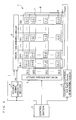
- a liquid crystal display apparatus of the present invention includes a liquid crystal display panel 1, a scan line driving circuit 2, a signal line driving circuit 3, a source signal generating section 4, a counter electrode voltage (Vcom) generating circuit 5, and a control section 6 as illustrated in Fig. 2 .
- the liquid crystal display panel 1 includes a pixel electrode substrate 7, a counter substrate 8 so as to be provided parallel to and face the pixel electrode substrate 7, and a liquid crystal (not illustrated) filled in a space between the pixel electrode substrate 7 and the counter substrate 8.
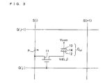
- a plurality of scan lines G (0)... G (J) and a plurality of signal lines S (0)... S (I) are provided so as to intersect with one another and pixels P ... are provided in matrix, respectively.
- a pixel P is provided in an area surrounded by adjacent scan lines G (j) and G (j-1) and adjacent signal lines S (i) and S (i+1).
- the pixel P includes a TFT (Thin Film Transistor) 11 serving as a switching element, and a liquid crystal capacitor C LC .
- TFT Thin Film Transistor
- a gate is connected to the scan line G (j) and a source signal is supplied to the signal line S (i).
- the liquid crystal capacitor C LC includes a pixel electrode 12 connected to the TFT 11, a counter electrode 13 facing the pixel electrode 12, and a liquid crystal 14 sandwiched by the pixel electrode 12 and the counter electrode 13.
- the counter electrode 13 is provided on the counter substrate 8 so as to be shared by all of the pixels P.
- the pixel electrode 12 is connected to the signal line S (i) via a source and a drain of the TFT 11.
- the gate of the TFT 11 is connected to the scan line G (j).
- the counter electrode 13 receives a counter electrode voltage Vcom released from the counter electrode voltage (Vcom) generating circuit 5. Since this causes a voltage difference between a signal voltage of a source signal Vs supplied from the signal line S (i) and a counter electrode voltage Vcom to be applied to the liquid crystal capacitor C LC while the TFT 11 is turned ON, a transmittance or a reflection rate of the liquid crystal is modulated. This allows the pixels P... to display an image corresponding to an inputted image data. Also, electric charge accumulated by the liquid crystal capacitor C LC is retained in each of the pixels P for a certain period of time. This allows a display of an image to be maintained in accordance with the electric charge even after the TFT is turned OFF.
- the following description deals with an example of changing the counter electrode voltage and the source voltage.
- a source voltage is fixed in accordance with a certain tone.
- a high voltage for tone 0 is set to 8.5 V and a low voltage for tone 0 is set to 7.5 V.
- a counter electrode voltage is fixed to 7.5 V by taking into consideration a lead-in voltage due to voltage fluctuation in gate electrode e.g. 0.5 V.
- the effective voltages to be applied to the pixel which are affected by the voltage fluctuation in the gate electrode, are 8.0 V for the high voltage side and 7.0 V for the low voltage side.
- + 0.5 V and - 0.5 V higher and lower than the counter electrode voltage are applied to a pixel as the effective voltages.
- a plane burning by shifting the counter electrode voltage from an optimum value by a shift amount, for example, of 1 V, which shift amount is changed between +1 V and -1 V alternately.
- the plane burning refers to a phenomenon in which, in a case where a state illustrated in Fig. 15 (a) is displayed for a long time, and is then changed into a half tone display, in a normally black mode, for example, a black display is retained brightly in an original area of the black display.
- the black display becomes blur when it is changed into a half tone display.
- a white display part becomes bright due to the fact that liquid crystal molecules remain tilted in the white display part and
- a black display part becomes bright due to the burning in the black display part caused by a counter electrode voltage. Therefore, it is possible to prevent a plane burning only by shifting the counter electrode voltage from the optimum value in a case where the vertical alignment control power is weak in the normally black mode (see Fig. 18 (a) and Fig. 18 (b) ).
- a control section 6 includes a counter for counting and determining that the time corresponding to an n-frame has elapsed.
- a predetermined source voltage or counter electrode voltage is changed.
- the voltage having the positive polarity and the voltage having the negative polarity which have an identical effective voltage for an identical tone value, are applied to the pixel between the counter electrode and the pixel electrode, and so become symmetric with respect to the counter electrode voltage.
- a low voltage having the positive polarity and a low voltage having the negative polarity are applied to a pixel for a black display. This causes an occurrence of the edge burning when a fixed pattern, after having been displayed for a long time, is changed into a half tone display.
- voltages of, for example, ⁇ 0.5 V are applied to the pixel.
- an embodiment of the present invention is arranged so that an effective voltage having the positive polarity and an effective voltage having the negative polarity, for an identical tone value, are asymmetrically applied to a pixel P between a counter electrode 13 and a pixel electrode 12.
- a counter electrode voltage Vcom-A is shifted by 0.3 V so as to have higher positive polarity than a conventional counter electrode voltage. This causes the voltage having the negative polarity to have a voltage of - 0.8 V.
- the edge burning is less likely to emerge because the electric field in the cell thickness direction becomes strong due to the increase in voltage to be applied to the pixel P.
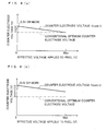
- Fig. 4 shows a relation between (i) an onset time of the edge burning in tone 0, i.e., at the lowest voltage and (ii) a shift amount from the optimum value of the counter electrode voltage.
- the onset time of the edge burning means how long it would take to recognize the edge burning visually.
- the onset time of the edge burning is getting longer for the shift amount of 0.3 V or more. Namely, it is clear that the shift amount of 0.3 V or more has an effect on alleviation of the edge burning.
- the voltage having the positive polarity and the voltage having the negative polarity which have symmetric effective voltages with respect to the counter electrode voltage, are applied to a pixel. Therefore, in a case of a low tone in which the edge burning occurs outstandingly, especially in a case where asymmetric effective voltages of less than ⁇ 0.8 V are applied to a pixel, it is impossible to secure symmetric effective voltages of 0.8 V for the positive and negative polarities. Note that for tones in which effective voltages of not less than ⁇ 0.8 V are applied to a pixel, it is possible to apply to the pixel the effective voltages of 0.8 V or more which are symmetric in the positive and negative polarities.
- the edge burning is immaterial and presents no problem.
- the voltages of 0.8 V or more having the positive and negative polarities are applied to a pixel, decline in contrast becomes large, which is not preferable. Therefore, in view of preventing decline in contrast, it is preferable that either the voltage having the positive polarity or the voltage having the negative polarity is 0.8 V or more.
- a counter electrode voltage or a source voltage is shifted from the optimum value of the counter electrode voltage Vcom so that the effective voltages of 0.8 V or more are applied to a pixel.
- Vcom the counter electrode voltage
- the shift amount from the optimum value of the counter electrode voltage Vcom is set to 0.3 V.
- a shift direction is not limited to either in the positive or negative polarity to attain the object. Note that Fig. 1 and Fig. 7 through Fig. 11 (later described) deals with a case where the optimum counter electrode is shifted toward the positive polarity.
- the shift amount from the optimum value of the counter electrode voltage Vcom is 2.0 V or less.
- a shift amount of more than 2.0 V causes a reduction in contrast and an increase in flicker.
- the counter electrode voltage Vcom is shifted by 0.3 V toward the positive polarity from a voltage (an optimum counter electrode voltage Vcom) causing the effective voltage having the positive polarity and the effective voltage having the negative polarity to be symmetrically applied to the pixel P.
- the counter electrode voltage Vcom is shifted by 0.3 V or more toward the positive polarity from the voltage causing the effective voltage having the positive polarity and the effective voltage having the negative polarity to be symmetrically applied to the pixel P so that the effective voltage having the negative polarity is higher than the effective voltage having the positive polarity, for an identical tone to be applied to the pixel P.
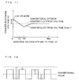
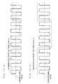
- the following description deals with how to calculate the optimum voltage of the counter electrode 13. For example, in bright tones, it is possible to find the optimum voltage of the counter electrode 13 by displaying a flicker pattern. Note that the voltage minimizing the flicker is the optimum voltage. In a case of black display, i.e., tone 0 in the normally black mode, however, no flicker is correctly observed even though the counter electrode 13 is shifted from the optimum voltage. In this case, for example as illustrated in Fig. 5 , an optimum voltage of the counter electrode 13 is found based on transition of black-level luminance. According to an example in Fig. 5 , the black-level luminance has the lowest voltage of 5.9 V. Therefore, the optimum voltage of the counter electrode 13 is 5.9 V in case of a current source voltage for tone 0. Note that when the source voltage Vs for tone 0 is shifted, the optimum voltage of the counter electrode 13 is also shifted.
- Fig. 6 illustrates ladder resistor 4e in the source signal generating section 4.
- VH 0 through VH 255 are applied voltages for the positive polarity and VL 0 through VL 255 are applied voltages for the negative polarity.
- the present embodiment is arranged so that asymmetric voltages are applied to the pixel P only for low voltages, by adjusting resistances of the resistors for the applied voltage VH 0 through VH 63 and VL 0 through VL 63 (circled resistances in Fig. 6 ) without changing the total resistance of R total.
- an asymmetric source voltage is supplied by the ladder resistor 4e in the source signal generating section 4 serving as the effective voltage control section.
- the counter electrode voltage Vcom can be set to, for example, 7.5 V independently by switching and/or sliding with the use of changing-over switches in the counter electrode voltage (Vcom) generating circuit 5 serving as the effective voltage control section.
- a tone falls within a range from 0 to 255.
- the present invention is not limited to this tone range.
- the counter electrode voltage Vcom-A is shifted by 0.3 V toward the positive polarity from the counter electrode voltage causing the effective voltage having the positive polarity and the effective voltage having the negative polarity to be symmetrically applied to the pixel P for all the tones.
- a shift amount which was less likely to cause the edge burning is 0.3 V or more according to experiments. Therefore, in the present embodiment, the edge burning surly becomes less likely to occur by shifting either the counter electrode voltage Vcom or the source voltage Vs by 0.3 V or more from a voltage causing the effective voltage having the positive polarity and the effective voltage having the negative polarity to be symmetrically applied to the pixel P.
- the present invention is not limited to this.
- a first effective voltage V1 which is lower than half of the maximum effective voltage, more specifically, for voltages of more than ⁇ 0.8 V
- the counter electrode voltage Vcom is set to the same voltage as that conventionally set.
- an axis of ordinate shows the optimum counter electrode voltage, i.e., a counter electrode voltage causing the flicker to be minimum, or the luminance to have a minimum or maximum value.
- the edge burning occurs for low effective voltages. Therefore, when the asymmetricity is reduced for the effective voltages which are higher than the first effective voltage V1, it is possible that the relation between the effective voltages and the tones gets close to a conventional relation in which an effective voltage having the positive polarity and an effective voltage having the negative polarity are symmetric.
- a liquid crystal display apparatus of the present embodiment for example, as illustrated in Fig. 8(a) , effective voltages for an identical tone to be applied to the pixels P between the counter electrodes 13 and the pixel electrodes 12 may be controlled so that an effective voltage having the positive polarity and an effective voltage having the negative polarity are shifted by 0.3 V or more from each other and are asymmetrically applied to the pixel, for a tone at which a minimum effective voltage is applied pixel and the asymmetricity may be reduced more as a tone is changed from a tone for a lowest effective voltage to a tone corresponding to an effective voltage which is higher than the lowest effective voltage.
- the counter electrode voltage Vcom is set to the same voltage as that conventionally set.
- an axis of ordinate shows the optimum counter electrode voltage, i.e., a counter electrode voltage causing the flicker to be minimum, or the luminance to have a minimum or maximum value.
- This arrangement may be realized by adjusting a certain source voltage.
- the arrangement is realized by a source voltage, for example, which is capable of controlling and adjusting a plurality of tone voltages.
- voltages to be applied to the pixel P for the black display in the normally black mode are asymmetric so that a voltage become higher than that conventionally applied in one side of the polarities. This causes the electric field to become strong in the cell thickness (vertical) direction. As a result, it is possible to prevent the movement of the impurities in the display panel in lateral directions, which leads the edge burning to be less likely to occur.
- the asymmetricity is reduced as the tone is changed from a tone for the lowest effective voltages to a tone for voltages which are higher than the lower lowest effective voltages. This allows the relation between the effective voltage and the tones to get close to a conventional relation in which an effective voltage having the positive polarity and an effective voltage having the negative polarity are symmetric.
- a liquid crystal of the present embodiment for example as illustrated in Fig. 9 (a) , it is possible to adjust a source voltage for each of the tones so that the asymmetricity is reduced as the effective voltage is changed from the lowest effective voltage to a second effective voltage V2, i.e. ⁇ 0.8 V, which is higher than the lowest effective voltage.
- the counter electrode voltage Vcom is set to the same voltage as that conventionally set.
- the source voltage is adjusted, it is possible to have an optimum counter electrode voltage Vcom-D which is changed as illustrated in Fig. 9 (a) .
- an axis of ordinate shows the optimum counter electrode voltage, i.e., a counter electrode voltage causing the flicker to be minimum, or the luminance to have a minimum or maximum value.
- the asymmetricity is gradually reduced up to the second effective voltage V2 which is higher than the lowest effective voltage. Therefore, it is possible to prevent the movement of the impurities in the liquid crystal panel 1 in lateral directions up to the second effective voltage V2 which causes the asymmetricity to be maintained, thereby preventing the edge burning.
- asymmetricity of an effective voltage having the positive polarity and an effective voltage having the negative polarity which are applied to the pixel becomes greater as the effective voltage gets closer to the maximum effective voltage from a third effective voltage V3 which is higher than the second effective voltage V2 and is also higher than half of the maximum effective voltage.
- the counter electrode voltage Vcom is set to the same voltage as that conventionally set.
- an axis of ordinate shows the optimum counter electrode voltage i.e., a counter electrode voltage causing the flicker to be minimum, or the luminance to have a minimum or maximum value.
- an effective voltage having the positive polarity and an effective voltage having the negative polarity are asymmetrically applied to the pixel P while an axis of symmetry is shifted toward the opposite polarity for a fourth effective voltage V4 which is higher than the second effective voltage V2. According to the liquid crystal display apparatus, it is possible to reduce the asymmetricity for voltages of higher than the fourth effective voltage V4.
- the effective voltage having the positive polarity and the effective voltage having the negative polarity are asymmetrically applied to the pixel P in the normally black mode
- the effective voltage having the positive polarity and the effective voltage having the negative polarity are asymmetrically applied to the pixel P in the normally white mode.
- the effective voltage having the positive polarity and the effective voltage having the negative polarity whose white display luminance is not more than about 5% or whose transmittance is not more than about 5 %, are asymmetrically applied to the pixel P in the normally black mode
- the effective voltage having the positive polarity and the effective voltage having the negative polarity whose white display luminance is not less than about 95% or whose transmittance is not less than about 95%, are asymmetrically applied to the pixel P in the normally white mode.
- the effective voltages to be applied to the pixel P are low. Therefore, it is possible to provide a liquid crystal display apparatus which can prevent the edge burning which would occur when a display of a fixed pattern, after having been displayed for a long time, is changed to a half tone display.
- the range that the white display luminance or the transmittance is not more than about 5% is defined because the flicker is hard to recognize. It is more preferable that the white display luminance or the transmittance is not more than 2%.
- the range that white display luminance or the transmittance is not less than about 95% is defined because the flicker is hard to recognize. It is more preferable that the white display luminance or the transmittance is not less than about 98%.
- the counter electrode voltage (Vcom) generating circuit 5 may control the effective voltages by a single polarity driving instead of a polarity inversion driving when the effective voltages of not less than 0.3 V to be applied to the pixels P are asymmetrical.
- the applied voltage may have a single polarity when the counter electrode voltage Vcom is largely shifted.
- the counter electrode voltage (Vcom) generating circuit 5 may shift, for every plural frames or for every plural fields, counter electrode voltages Vcom-G and Vcom-G' by 0.3 V or more alternately toward the positive polarity and the negative polarity from an effective voltage causing the voltage having the positive polarity and the voltage having the negative polarity to be asymmetrically applied to the pixel, in a certain pixel voltage range or all the pixel voltage ranges.
- the plane burning worsens.
- the polarities toward which the counter electrode voltage is shifted are alternately changed at a certain interval. This allows preventing of the plane burning.
- a counter electrode voltage (Vcom) generating circuit 5 may cause each of the counter electrode voltages Vcom-G and Vcom-G' to change to alternately have a shift toward the positive polarity and a shift toward the negative polarity at a certain interval.
- the counter electrode voltage Vcom is changed so as to alternately have a shift toward the positive polarity and a shift toward the negative polarity.
- the present embodiment is, however, not limited to this.
- the source signal generating section 4 may cause the source voltage Vs to change to alternately have a shift toward the positive polarity and a shift toward the negative polarity at a certain interval.
- the counter electrode voltage (Vcom) generating circuit 5 may cause each of the counter electrode voltages Vcom-G and Vcom-G' to change in sync with turning on the liquid crystal display panel so as to alternately or randomly have a shift toward the positive polarity and a shift toward the negative polarity.
- the counter electrode voltage (Vcom) generating circuit 5 changes the polarities of the counter electrode voltages Vcom alternately toward the positive polarity and the negative polarity, after the display is changed to the entire black display, entire white display, or entire gray display.
- the counter electrode voltage (Vcom) generating circuit 5 may change the polarities of the counter electrode voltage Vcom at an interval of about one hour to ten days, so that the effective voltage having the positive polarity and the effective voltage having the negative polarity are asymmetrically applied.
- a shift toward the positive polarity and a shift toward the negative polarity are changed alternately in an interval of about one hour to about ten days.
- the counter electrode voltage (Vcom) generating circuit 5 or the source signal generating circuit 4 applies a voltage to the liquid crystal 14 in the pixel P between a pair of substrates, i.e., the pixel electrode substrate 7 and the counter substrate 8 in a liquid crystal panel 1.
- the effective voltage control section shifts the counter electrode voltage by 0.3 V or more toward the positive polarity from a voltage causing the effective voltage having the positive polarity and the effective voltage having the negative polarity, for an identical tone, to be symmetrically applied to the pixel so that the effective voltage having the negative polarity is higher than the effective voltage having the positive polarity to be applied to the pixel.
- the edge burning surly becomes less likely to happen, for example, by shifting the counter electrode voltage by 0.3 V or more toward the positive polarity from a counter electrode voltage causing the effective voltage having the positive polarity and the effective voltage having the negative polarity, for an identical tone, to be symmetrically applied to the pixel so that the effective voltage having the negative polarity is higher than the effective voltage having the positive polarity to be applied to the pixel.
- the effective voltages control section may control the effective voltages for an identical tone so that an effective voltage having the positive polarity and an effective voltage having the negative polarity are asymmetrically applied to the pixels between the counter electrodes and the pixel electrodes, even for effective voltages of higher than the first effective voltage, and may reduce asymmetricity for voltages of higher than the first effective voltage.
- the edge burning occurs for low effective. Therefore, when the asymmetricity is reduced for the effective voltages which are higher than the first effective voltages, it is possible that the relation between the effective voltages and the tones gets close to a conventional relation.
- the effective voltage control section may reduce the asymmetricity as the effective voltage is changed from the lowest effective voltage to a second effective voltage which is higher than the lowest effective voltage.
- the asymmetricity is gradually reduced up to the second effective voltage which is higher than the lowest effective voltage. Therefore, it is possible to prevent the movement of the impurities in the liquid crystal panel in lateral directions up to the second effective voltage which causes the asymmetricicty to be maintained, thereby preventing the edge burning.
- the effective voltage control section may cause the effective voltage having the positive polarity and the effective voltage having the negative polarity to be symmetrically applied to the pixel for an effective voltage which is higher than the second effective voltage.
- the effective voltage control section may cause the asymmetricity of the effective voltage having the positive polarity and the effective voltage having the negative polarity which are applied to the pixel to become greater from a third effective voltage, which is higher than the second effective voltage and is also higher than half of the maximum effective voltage, to the maximum effective voltage.
- the effective voltage control section may cause the effective voltage having the positive polarity and the effective voltage having the negative polarity to be asymmetrically applied to the pixel while an axis of symmetry is shifted toward the opposite polarity, for a fourth effective voltage which is higher than the second effective voltage, and causes the asymmetricity to be small, for an effective voltage which is higher than the fourth effective voltage.
- the effective voltage control section may cause the effective voltage having the positive polarity and the effective voltage having the negative polarity, whose white display luminance is not more than 5% or whose transmittance is not more than 5%, to be asymmetrically applied to the pixel in a normally black mode, whereas the effective voltage having the positive polarity and the effective voltage having the negative polarity, whose white display luminance is not less than about 95% or whose transmittance is not less than about 95%, to be asymmetrically applied to the pixel in a normally white mode.
- the effective voltage having the positive polarity and the effective voltage having the negative polarity whose white display luminance is not more than about 5% or whose transmittance is not more than about 5 %, are asymmetrically applied to the pixel in the normally black mode
- the effective voltage having the positive polarity and the effective voltage having the negative polarity whose white display luminance is not less than about 95% or whose transmittance is not less than about 95%, are asymmetrically applied to the pixel in the normally white mode.
- the effective voltages to be applied to the pixel P are low. Therefore, it is possible to provide a liquid crystal display apparatus which can prevent the edge burning which would occur when a display of a fixed pattern, after having been displayed for a long time, is changed to a half tone display.
- the range that the white display luminance or the transmittance is not more than about 5% is defined because the flicker is hard to recognize. It is more preferable that the white display luminance or the transmittance is not more than 2%.
- the range that white display luminance or the transmittance is not less than about 95% is defined because the flicker is hard to recognize. It is more preferable that the white display luminance or the transmittance is not less than about 98%.
- the effective voltage control section may control the effective voltage by a single polarity driving instead of a polarity inversion driving for a certain pixel voltage region while the effective voltages to be applied to the pixel are asymmetrical.
- the applied voltage may have a single polarity when the counter electrode voltage or the source voltage is largely shifted.
- the effective voltage control section may shift, for every plural frames or for every plural fields, the counter electrode voltage or the source voltage by 0.3 V or more alternately toward the positive polarity and the negative polarity from an effective voltage causing the voltage having the positive polarity and the voltage having the negative polarity to be symmetrically applied to the pixel, in a certain pixel voltage range.
- the effective voltage control section may shift the counter electrode voltage or the source voltage alternately toward the positive polarity and the negative polarity at a certain cycle, so that the effective voltage having the positive polarity and the effective voltage having the negative polarity are asymmetrically applied.
- the effective voltage control section may change the counter electrode voltage or the source voltage in sync with turning on the liquid crystal display panel so that the counter electrode voltage or the source voltage alternately or randomly has a shift toward the positive polarity and a shift toward the negative polarity, so as to perform the asymmetrical application of the effective voltage having the positive polarity and the effective voltage having the negative polarity.
- the effective voltage control section may shift the counter electrode voltage or the source voltage alternately toward the positive polarity and the negative polarity, while displaying an entire black display, an entire white display, or an entire gray display which includes an single color display of red (R), green (G), and blue (B), or a still image.
- the effective voltage control section may shift the counter electrode voltage or the source voltage alternately toward the positive polarity and the negative polarity in an interval of about one hour to ten days, so that the effective voltage having the positive polarity and the effective voltage having the negative polarity are asymmetrically applied.
- a shift toward the positive polarity and a shift toward the negative polarity are changed alternately in an interval of about one hour to ten days.
- the effective voltage control section may apply a voltage to a liquid crystal in a pixel between a pair of substrates, i.e., a pixel electrode substrate and a counter substrate in a liquid crystal panel.
- the present invention is applicable to a VA or a TN type liquid crystal display apparatus in which a voltage having the positive polarity and a voltage having the negative polarity are alternately applied to a pixel between a counter electrode and a pixel electrode, and is applicable to a method for driving the same.
Landscapes
- Physics & Mathematics (AREA)
- Engineering & Computer Science (AREA)
- General Physics & Mathematics (AREA)
- Crystallography & Structural Chemistry (AREA)
- Chemical & Material Sciences (AREA)
- Theoretical Computer Science (AREA)
- Computer Hardware Design (AREA)
- Nonlinear Science (AREA)
- Mathematical Physics (AREA)
- Optics & Photonics (AREA)
- Power Engineering (AREA)
- Control Of Indicators Other Than Cathode Ray Tubes (AREA)
- Liquid Crystal (AREA)
- Liquid Crystal Display Device Control (AREA)
Applications Claiming Priority (2)
| Application Number | Priority Date | Filing Date | Title |
|---|---|---|---|
| JP2006127054 | 2006-04-28 | ||
| PCT/JP2007/057648 WO2007125738A1 (ja) | 2006-04-28 | 2007-04-05 | 液晶表示装置及びその駆動方法 |
Publications (2)
| Publication Number | Publication Date |
|---|---|
| EP2015286A1 true EP2015286A1 (de) | 2009-01-14 |
| EP2015286A4 EP2015286A4 (de) | 2011-07-06 |
Family
ID=38655273
Family Applications (1)
| Application Number | Title | Priority Date | Filing Date |
|---|---|---|---|
| EP07741084A Withdrawn EP2015286A4 (de) | 2006-04-28 | 2007-04-05 | Flüssigkristallanzeigevorrichtung und verfahren zu ihrer ansteuerung |
Country Status (5)
| Country | Link |
|---|---|
| US (1) | US8174474B2 (de) |
| EP (1) | EP2015286A4 (de) |
| JP (1) | JP5020944B2 (de) |
| CN (1) | CN101432794B (de) |
| WO (1) | WO2007125738A1 (de) |
Families Citing this family (10)
| Publication number | Priority date | Publication date | Assignee | Title |
|---|---|---|---|---|
| CN101772800B (zh) * | 2007-08-02 | 2013-01-02 | 夏普株式会社 | 液晶显示装置及其驱动方法、以及驱动电路 |
| KR100920376B1 (ko) * | 2007-12-21 | 2009-10-07 | 엘지디스플레이 주식회사 | 액정표시장치와 그 구동방법 |
| US8698728B2 (en) * | 2009-11-02 | 2014-04-15 | Atmel Corporation | Apparatus for integrated backlight and dynamic gamma/VCOM control on silicon chips |
| WO2011065063A1 (ja) * | 2009-11-27 | 2011-06-03 | シャープ株式会社 | 液晶表示装置および液晶表示装置の駆動方法 |
| CN102201206B (zh) * | 2010-03-26 | 2012-10-31 | 北京京东方光电科技有限公司 | 调整像素电压对称的方法及装置 |
| JP5608112B2 (ja) * | 2011-01-28 | 2014-10-15 | 株式会社ジャパンディスプレイ | シャッタメガネ |
| JP2016218168A (ja) * | 2015-05-18 | 2016-12-22 | キヤノン株式会社 | 駆動装置、表示装置および電子機器 |
| CN105118457B (zh) * | 2015-09-11 | 2017-12-08 | 昆山龙腾光电有限公司 | 显示面板闪烁的校正方法、校正装置 |
| CN108269544B (zh) * | 2018-01-31 | 2020-08-25 | 京东方科技集团股份有限公司 | 闪烁漂移优化电路及显示面板、显示装置 |
| CN113345385B (zh) * | 2021-05-31 | 2022-03-22 | 北海惠科光电技术有限公司 | 显示面板的校正方法、装置、计算机设备和存储介质 |
Family Cites Families (25)
| Publication number | Priority date | Publication date | Assignee | Title |
|---|---|---|---|---|
| JPH0572997A (ja) * | 1991-09-13 | 1993-03-26 | Sanyo Electric Co Ltd | 液晶表示装置の駆動方法 |
| JPH05119742A (ja) * | 1991-10-25 | 1993-05-18 | Nec Corp | 液晶パネル駆動方法 |
| JP2997356B2 (ja) | 1991-12-13 | 2000-01-11 | 京セラ株式会社 | 液晶表示装置の駆動方法 |
| JPH0720440A (ja) | 1993-06-30 | 1995-01-24 | Kyocera Corp | 液晶表示装置 |
| JPH0792937A (ja) * | 1993-07-29 | 1995-04-07 | Hitachi Ltd | 液晶駆動方法と液晶表示装置 |
| KR100343513B1 (ko) | 1993-07-29 | 2003-05-27 | 히다찌디바이스엔지니어링 가부시기가이샤 | 액정구동방법과액정표시장치 |
| JPH07199867A (ja) * | 1993-12-28 | 1995-08-04 | Nec Corp | アクティブマトリクス型液晶表示装置の駆動法 |
| JPH08278515A (ja) | 1995-04-07 | 1996-10-22 | Matsushita Electric Ind Co Ltd | 液晶表示装置 |
| JP3471152B2 (ja) * | 1995-11-30 | 2003-11-25 | アルプス電気株式会社 | 液晶表示素子および液晶表示素子の駆動方法 |
| CN1166068C (zh) * | 1996-02-09 | 2004-09-08 | 精工爱普生株式会社 | D/a变换器及其设计方法、液晶屏用基片和液晶显示装置 |
| JP3657080B2 (ja) * | 1997-03-26 | 2005-06-08 | 株式会社アドバンスト・ディスプレイ | 液晶表示装置の駆動方法 |
| US6992718B1 (en) * | 1998-08-31 | 2006-01-31 | Matsushita Electric Industrial Co., Ltd. | Illuminating apparatus, display panel, view finder, video display apparatus, and video camera mounting the elements |
| WO2001057837A1 (en) * | 2000-02-02 | 2001-08-09 | Seiko Epson Corporation | Method for driving electrooptical device, drivinng circuit, and electrooptical device, and electronic apparatus |
| JP3579766B2 (ja) | 2000-05-26 | 2004-10-20 | 株式会社アドバンスト・ディスプレイ | 液晶表示装置の駆動方法 |
| JP2002251170A (ja) | 2001-02-23 | 2002-09-06 | Matsushita Electric Ind Co Ltd | 液晶表示装置 |
| JP2002358056A (ja) * | 2001-03-28 | 2002-12-13 | Seiko Epson Corp | 画像表示装置および共通信号供給方法 |
| JP3655217B2 (ja) * | 2001-06-21 | 2005-06-02 | 株式会社東芝 | 液晶表示素子の駆動方法 |
| JP2005512133A (ja) * | 2001-12-05 | 2005-04-28 | コーニンクレッカ フィリップス エレクトロニクス エヌ ヴィ | 通常モードおよび待機モードにおける液晶表示装置の駆動方法 |
| KR100848092B1 (ko) | 2002-03-06 | 2008-07-24 | 삼성전자주식회사 | 액정 표시 장치 및 그의 구동 방법 |
| JP2004069886A (ja) * | 2002-08-05 | 2004-03-04 | Canon Inc | 液晶表示装置 |
| JP4330871B2 (ja) * | 2002-11-28 | 2009-09-16 | シャープ株式会社 | 液晶駆動装置 |
| TWI298864B (en) * | 2003-04-18 | 2008-07-11 | Himax Tech Inc | Driving method fro cholesteric texture liquid crystal display |
| JP3861860B2 (ja) * | 2003-07-18 | 2006-12-27 | セイコーエプソン株式会社 | 電源回路、表示ドライバ及び電圧供給方法 |
| US7050027B1 (en) * | 2004-01-16 | 2006-05-23 | Maxim Integrated Products, Inc. | Single wire interface for LCD calibrator |
| TWI339369B (en) * | 2006-06-14 | 2011-03-21 | Au Optronics Corp | Method of driving a liquid crystal display |
-
2007
- 2007-04-05 CN CN2007800152337A patent/CN101432794B/zh not_active Expired - Fee Related
- 2007-04-05 US US12/298,716 patent/US8174474B2/en active Active
- 2007-04-05 JP JP2008513126A patent/JP5020944B2/ja not_active Expired - Fee Related
- 2007-04-05 WO PCT/JP2007/057648 patent/WO2007125738A1/ja not_active Ceased
- 2007-04-05 EP EP07741084A patent/EP2015286A4/de not_active Withdrawn
Also Published As
| Publication number | Publication date |
|---|---|
| WO2007125738A1 (ja) | 2007-11-08 |
| CN101432794A (zh) | 2009-05-13 |
| JPWO2007125738A1 (ja) | 2009-09-10 |
| CN101432794B (zh) | 2011-04-27 |
| US8174474B2 (en) | 2012-05-08 |
| US20090167665A1 (en) | 2009-07-02 |
| EP2015286A4 (de) | 2011-07-06 |
| JP5020944B2 (ja) | 2012-09-05 |
Similar Documents
| Publication | Publication Date | Title |
|---|---|---|
| US8174474B2 (en) | Liquid crystal display apparatus and method for driving the same | |
| US10535315B2 (en) | Display device, method for driving display device and method for minimizing afterimage of display device | |
| EP2317501B1 (de) | Verfahren und Vorrichtung zur Ansteuerung einer Flüssigkristallanzeige | |
| US7764262B2 (en) | Liquid crystal display device and method of driving the same | |
| KR101108343B1 (ko) | 액정표시장치 | |
| US10373576B2 (en) | Liquid crystal display driving apparatus including pixel voltage driving circuit for providing periodical pulse high-voltage signal | |
| US20040263743A1 (en) | Liquid crystal display device and method for driving the same | |
| US8885131B2 (en) | Liquid crystal display device | |
| KR20040084443A (ko) | 액정표시장치 | |
| CN102667907A (zh) | 液晶显示装置和液晶显示装置的驱动方法 | |
| JP2003295157A (ja) | 液晶表示装置 | |
| JP4163678B2 (ja) | 液晶表示装置の駆動方法 | |
| US8054275B2 (en) | Liquid crystal driving circuit and method with correction coefficients based on current and previous frame gradation ranges | |
| JP2013137418A (ja) | 液晶表示装置 | |
| US7212180B2 (en) | Method of driving liquid crystal display device | |
| KR20010107715A (ko) | 액정표시장치의 구동방법 | |
| US8384703B2 (en) | Liquid crystal display device | |
| KR20030055385A (ko) | 액정표시장치의 구동 방법 | |
| KR20050068605A (ko) | 액정표시장치의 구동방법 | |
| US10114255B2 (en) | Display apparatus | |
| US20110169880A1 (en) | Liquid crystal display device and method for driving liquid crystal display device | |
| KR100879214B1 (ko) | 액정표시소자 | |
| KR20030056526A (ko) | 액정 표시 장치의 구동 방법 | |
| KR20000014529A (ko) | 평면 구동 방식 액정 표시 장치 | |
| KR20130041443A (ko) | 액정 표시장치 및 그 구동방법 |
Legal Events
| Date | Code | Title | Description |
|---|---|---|---|
| PUAI | Public reference made under article 153(3) epc to a published international application that has entered the european phase |
Free format text: ORIGINAL CODE: 0009012 |
|
| 17P | Request for examination filed |
Effective date: 20081023 |
|
| AK | Designated contracting states |
Kind code of ref document: A1 Designated state(s): AT BE BG CH CY CZ DE DK EE ES FI FR GB GR HU IE IS IT LI LT LU LV MC MT NL PL PT RO SE SI SK TR |
|
| AX | Request for extension of the european patent |
Extension state: AL BA HR MK RS |
|
| A4 | Supplementary search report drawn up and despatched |
Effective date: 20110608 |
|
| DAX | Request for extension of the european patent (deleted) | ||
| 17Q | First examination report despatched |
Effective date: 20130424 |
|
| STAA | Information on the status of an ep patent application or granted ep patent |
Free format text: STATUS: THE APPLICATION IS DEEMED TO BE WITHDRAWN |
|
| 18D | Application deemed to be withdrawn |
Effective date: 20130905 |