EP2015324B1 - Condensateur a film - Google Patents
Condensateur a film Download PDFInfo
- Publication number
- EP2015324B1 EP2015324B1 EP07742477.8A EP07742477A EP2015324B1 EP 2015324 B1 EP2015324 B1 EP 2015324B1 EP 07742477 A EP07742477 A EP 07742477A EP 2015324 B1 EP2015324 B1 EP 2015324B1
- Authority
- EP
- European Patent Office
- Prior art keywords
- dielectric film
- capacitor electrodes
- electrode pattern
- capacitor
- film
- Prior art date
- Legal status (The legal status is an assumption and is not a legal conclusion. Google has not performed a legal analysis and makes no representation as to the accuracy of the status listed.)
- Ceased
Links
Images


Classifications
-
- H—ELECTRICITY
- H01—ELECTRIC ELEMENTS
- H01G—CAPACITORS; CAPACITORS, RECTIFIERS, DETECTORS, SWITCHING DEVICES, LIGHT-SENSITIVE OR TEMPERATURE-SENSITIVE DEVICES OF THE ELECTROLYTIC TYPE
- H01G4/00—Fixed capacitors; Processes of their manufacture
- H01G4/32—Wound capacitors
-
- H—ELECTRICITY
- H01—ELECTRIC ELEMENTS
- H01G—CAPACITORS; CAPACITORS, RECTIFIERS, DETECTORS, SWITCHING DEVICES, LIGHT-SENSITIVE OR TEMPERATURE-SENSITIVE DEVICES OF THE ELECTROLYTIC TYPE
- H01G2/00—Details of capacitors not covered by a single one of groups H01G4/00-H01G11/00
- H01G2/14—Protection against electric or thermal overload
-
- H—ELECTRICITY
- H01—ELECTRIC ELEMENTS
- H01G—CAPACITORS; CAPACITORS, RECTIFIERS, DETECTORS, SWITCHING DEVICES, LIGHT-SENSITIVE OR TEMPERATURE-SENSITIVE DEVICES OF THE ELECTROLYTIC TYPE
- H01G4/00—Fixed capacitors; Processes of their manufacture
- H01G4/002—Details
- H01G4/005—Electrodes
-
- H—ELECTRICITY
- H01—ELECTRIC ELEMENTS
- H01G—CAPACITORS; CAPACITORS, RECTIFIERS, DETECTORS, SWITCHING DEVICES, LIGHT-SENSITIVE OR TEMPERATURE-SENSITIVE DEVICES OF THE ELECTROLYTIC TYPE
- H01G4/00—Fixed capacitors; Processes of their manufacture
- H01G4/002—Details
- H01G4/005—Electrodes
- H01G4/01—Form of self-supporting electrodes
-
- H—ELECTRICITY
- H01—ELECTRIC ELEMENTS
- H01G—CAPACITORS; CAPACITORS, RECTIFIERS, DETECTORS, SWITCHING DEVICES, LIGHT-SENSITIVE OR TEMPERATURE-SENSITIVE DEVICES OF THE ELECTROLYTIC TYPE
- H01G4/00—Fixed capacitors; Processes of their manufacture
- H01G4/002—Details
- H01G4/018—Dielectrics
- H01G4/06—Solid dielectrics
- H01G4/14—Organic dielectrics
- H01G4/18—Organic dielectrics of synthetic material, e.g. derivatives of cellulose
-
- H—ELECTRICITY
- H01—ELECTRIC ELEMENTS
- H01G—CAPACITORS; CAPACITORS, RECTIFIERS, DETECTORS, SWITCHING DEVICES, LIGHT-SENSITIVE OR TEMPERATURE-SENSITIVE DEVICES OF THE ELECTROLYTIC TYPE
- H01G2/00—Details of capacitors not covered by a single one of groups H01G4/00-H01G11/00
- H01G2/14—Protection against electric or thermal overload
- H01G2/16—Protection against electric or thermal overload with fusing elements
Definitions
- the present invention relates to a film capacitor having a roll of a first electrode pattern and a second electrode pattern which confront each other with a dielectric film sandwiched therebetween, a first terminal electrically connected to one end of the roll, and a second terminal electrically connected to the other end of the roll, and more particularly to a film capacitor which has both a self-healing function and a self-protection mechanism.
- Film capacitors having both a self-healing function and a self-protection mechanism are disclosed in Patent Documents 1 through 4, for example.
- the film capacitor disclosed in Patent Document 1 has a pair of capacitor electrodes which confront each other with a dielectric film sandwiched therebetween. At least one of the capacitor electrodes is formed by metal evaporation, and is divided into equally spaced or arbitrarily spaced intervals in the longitudinal direction of the film by a plurality of insulating grooves, thereby providing a plurality of segmented electrode banks.
- the segmented electrode banks comprise electrodes provided by a network of insulating grooves with a plurality of narrow current paths left therebetween.
- the capacitor electrodes sandwiching the dielectric film serve as a metalized film having 2 to 20 independent small electrodes arrayed in the longitudinal direction of the film and a plurality of independent small electrodes arrayed in the transverse direction of the film.
- the metalized film is rolled into a roll, and metal is thermal-sprayed to opposite end faces of the roll to form terminal electrodes, thus producing a capacitor element.
- One or more capacitor elements are encased into the film capacitor.
- the film capacitor disclosed in Patent Document 2 comprises a dielectric film and a metal-evaporated electrode disposed on the dielectric film.
- the metal-evaporated electrode has a plurality of divided electrodes arrayed in longitudinal and transverse directions thereof.
- the divided electrodes are segmented by non-electrode margins, and margin fuses having a fuse function are disposed in the margins.
- the margin fuses are superposed over margin fuses on upper and lower confronting electrodes.
- the film capacitor disclosed in Patent Document 3 is a capacitor sheet which comprises a dielectric capacitor sheet having a metal thin film thereon and rolled into a capacitor roll in the traveling direction of the dielectric capacitor sheet.
- the film capacitor includes a metalized region which includes the metal thin film with divisions therein.
- the metal thin film includes partial divisions formed in the transverse direction to the traveling direction of the capacitor sheet.
- the film capacitor disclosed in Patent Document 4 includes a pair of evaporated electrodes having divided electrodes connected parallel to each other through fuses and extending from a substantially transversely central region toward insulated margins in an effective electrode area providing a capacitance. Since the fuses and the divided electrodes are disposed closely to the insulated margins where reduced currents flow at positions away from components plated by thermal-sprayed metal, the heat produced by the fuses is reduced to lower a temperature rise.
- the divided electrodes are directly connected by the very narrow fuses to lead-out electrodes that are electrically connected to the terminals of the film capacitor.
- Document US 6 040 038 A discloses a film condenser and a metalized film for manufacturing the same.
- the metalized film comprises a base film formed from an insulating material, and a metal coating layer formed on the base film.
- a plurality of uncoated portions are formed as area partition margins in the metal coating layer so as to respectively form, in the metal coating layer, a plurality of electrode regions, a plurality of fuse connecting regions surrounded by two or more of the electrode regions, and a plurality of fuse portions.
- the fuse portions electrically connect each one of the fuse connecting regions with the electrode regions surrounding the one of the fuse connecting regions.
- the present invention has been made in view of the above problems. It is an object of the present invention to provide a film capacitor which has a sufficient heat radiation path, has both a self-healing function and a self-protection mechanism, and finds itself usable in various applications.
- the first capacitor electrodes and the third capacitor electrodes can be effectively utilized as heat radiation paths. Accordingly, the film capacitor has sufficient heat radiation paths, has both a self-healing function and a self-protection mechanism, has an increased allowable current value, and finds itself usable in various applications.
- the film capacitor according to the present invention has sufficient heat radiation paths, has both a self-healing function and a self-protection mechanism, and finds itself usable in various applications.
- Embodiments of film capacitors according to the present invention will be described below with reference to FIGS. 1 through 10 .
- first film capacitor 10A a film capacitor according to a first embodiment of the present invention
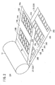
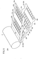
- first film capacitor 10A comprises a roll 12, a first terminal 14 electrically connected to an end of the roll 12, and a second terminal 16 electrically connected to the other end of the roll 12.
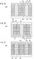
- the roll 12 includes a first electrode pattern 18A and a second electrode pattern 18B which are rolled in confronting relation to each other with a dielectric film 20 sandwiched therebetween.
- the roll 12 of the first film capacitor 10A comprises a first dielectric film 22A with the first electrode pattern 18A disposed on one side thereof and a second dielectric film 22B with the second electrode pattern 18B disposed on one side thereof.
- the first dielectric film 22A and the second dielectric film 22B are superposed one on the other such that the first electrode pattern 18A and the second electrode pattern 18B are kept out of contact with each other, and are rolled together.
- Each of the first dielectric film 22A and the second dielectric film 22B may be made of PP (polypropylene), PET (polyethylene terephthalate), PPS (polyphenylene sulfide), or the like.
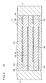
- the first dielectric film 22A and the second dielectric film 22B have a width Wa (see FIG. 2 ) in the range from 10 to 200 mm and a thickness ta (see FIG. 3 ) in the range from 2.7 to 30 ⁇ m.
- the first electrode pattern 18A and the second electrode pattern 18B may be made of aluminum, zinc, an alloy of aluminum and zinc, or the like.
- the first electrode pattern 18A and the second electrode pattern 18B should preferably have a thickness tb (see FIG. 3 ) which satisfies a surface resistance in the range from 1 to 20 ohms/mm 2 , and may be in the range from 100 to 1000 Angstroms, for example.
- the first film capacitor 10A has a capacitance value in the range from about several tens ⁇ F to several hundreds ⁇ F, a rated voltage of several hundreds V (DC), and a rated current of several tens A.
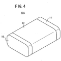
- the first film capacitor 10A is of a cylindrical shape as shown in FIG. 1 or a flat shape as shown in FIG. 4 .
- the first electrode pattern 18A has a first lead-out electrode 24A extending continuously in the longitudinal direction of the first dielectric film 22A, a plurality of first capacitor electrodes 26A extending substantially perpendicularly from the first lead-out electrode 24A, and a plurality of second capacitor electrodes 26B disposed between the first capacitor electrodes 26A and connected to the first capacitor electrodes 26A.
- the second electrode pattern 18B has a second lead-out electrode 24B extending continuously in the longitudinal direction of the second dielectric film 22B, a plurality of third capacitor electrodes 26C extending substantially perpendicularly from the second lead-out electrode 24B, and a plurality of fourth capacitor electrodes 26D disposed between the third capacitor electrodes 26C and connected to the third capacitor electrodes 26C.
- the width W4 of the fourth capacitor electrodes 26D along the longitudinal direction of the second dielectric film 22B is greater than the width W1 of the first capacitor electrodes 26A along the longitudinal direction of the first dielectric film 22A.
- the width W2 of the second capacitor electrodes 26B along the longitudinal direction of the first dielectric film 22A is greater than the width W3 of the third capacitor electrodes 26C along the longitudinal direction of the second dielectric film 22B.
- the first capacitor electrodes 26A of the first electrode pattern 18A and the fourth capacitor electrodes 26D of the second electrode pattern 18B are superposed one on the other with the first dielectric film 22A or the second dielectric film 22B being sandwiched therebetween.
- the second capacitor electrodes 26B of the first electrode pattern 18A and the third capacitor electrodes 26C of the second electrode pattern 18B are superposed one on the other with the first dielectric film 22A or the second dielectric film 22B being sandwiched therebetween.
- the first lead-out electrode 24A of the first electrode pattern 18A extends to a side edge 30a of the first dielectric film 22A such that the first lead-out electrode 24A is electrically connected to the first terminal 14.
- the second lead-out electrode 24B of the second electrode pattern 18B extends to a side edge 32b of the second dielectric film 22B (opposite to the side edge 30a) such that the second lead-out electrode 24B is electrically connected to the second terminal 16.
- the second capacitor electrodes 26B of the first electrode pattern 18A have a plurality of first sections 34 that are connected to opposite end faces 36a, 36b of the first capacitor electrodes 26A which extend transversely across the first dielectric film 22A, through narrow first fuses 38.
- the fourth capacitor electrodes 26D of the second electrode pattern 18B have a plurality of second sections 40 that are connected to opposite end faces 42a, 42b of the third capacitor electrodes 26C which extend transversely across the second dielectric film 22B, through narrow second fuses 44.
- the first film capacitor 10A When the first film capacitor 10A suffers a fault, the first sections 34 and the second sections 40 can individually be electrically disconnected. Therefore, the first film capacitor 10A is prevented from undergoing a large reduction in the capacitance upon the fault. Since the wide first capacitor electrodes 26A are disposed between the first fuses 38 and the first lead-out electrode 24A, and the wide third capacitor electrodes 26C are disposed between the second fuses 44 and the second lead-out electrode 24B, the first capacitor electrodes 26A and the third capacitor electrodes 26C can be effectively utilized as heat radiation paths. In other words, the first film capacitor 10A has sufficient heat radiation paths, has an increased allowable current value, and finds itself usable in various applications.
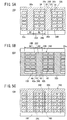
- a film capacitor lOAa according to a first modification is of a structure substantially similar to the first film capacitor 10A, but is different therefrom as to the structure of the first sections 34 and the second sections 40.
- Each of the first sections 34 comprises a plurality of first small sections 46 arrayed along the longitudinal direction of the first dielectric film 22A and connected through narrow third fuses 48.
- each of the second sections 40 comprises a plurality of second small sections 50 arrayed along the longitudinal direction of the second dielectric film 22B and connected by narrow fourth fuses 52.
- the first capacitor electrodes 26A and the third capacitor electrodes 26C can also be effectively utilized as heat radiation paths. Particularly, since the first sections 34 and the second sections 40 are divided into the first small sections 46 and the second small sections 50, the first small sections 46 and the second small sections 50 can individually be electrically disconnected when the film capacitor 10Aa suffers a fault. The film capacitor 10Aa is prevented from undergoing a large reduction in the capacitance upon the fault.
- a film capacitor 10Ab according to a second modification which illustrates an example useful for understanding the invention, is of a structure substantially similar to the film capacitor 10Aa according to the first modification, but is different therefrom as to the following features: Fifth fuses 54 that are narrower than the first capacitor electrodes 26A and wider than the first fuses 38 are disposed between the first lead-out electrode 24A and the first capacitor electrodes 26A of the first electrode pattern 18A. Similarly, sixth fuses 56 that are narrower than the third capacitor electrodes 26C and wider than the second fuses 44 are disposed between the second lead-out electrode 24B and the third capacitor electrodes 26C of the second electrode pattern 18B.
- the film capacitor 10Ab suffers a defect in a wide range including one of the first capacitor electrodes 26A, for example, the first capacitor electrodes 26A can individually be electrically disconnected. The film capacitor 10Ab is thus prevented from undergoing a large reduction in the capacitance upon the fault.
- a film capacitor lOAc according to a third modification is of a structure substantially similar to the first film capacitor 10A, but is different therefrom in that the side edges 30a, 30b of the first dielectric film 22A are of a wavy shape and the side edges 32a, 32b of the second dielectric film 22B are of a wavy shape.
- the wavy shapes are shown as being similar to a sine-wave shape in FIG. 8 , they may be a shape similar to a triangular shape, a semicircular shape, or the like.
- the first lead-out electrode 24A and the second lead-out electrode 24B are less liable to be exposed on the opposite ends of the roll 12, and may not well be electrically connected to the first terminal 14 and the second terminal 16.
- the ends of the roll 12 and the first and second terminals 14, 16 may have an adhesion problem.
- the side edges 30a, 30b of the first dielectric film 22A are of a wavy shape and the side edges 32a, 32b of the second dielectric film 22B are of a wavy shape, when they are rolled into the roll 12, the first lead-out electrode 24A and the second lead-out electrode 24B are more liable to be exposed on the opposite ends of the roll 12, and can well be electrically connected to the first terminal 14 and the second terminal 16, and the ends of the roll 12 can well adhere to the first and second terminals 14, 16. Accordingly, the film capacitor lOAc can prevent a local large current from flowing thereinto and hence is highly reliable in operation.
- second film capacitor 10B A film capacitor according to a second embodiment of the present invention (hereinafter referred to as "second film capacitor 10B") will be described below with reference to FIGS. 9 and 10 .
- the second film capacitor 10B is of essentially the same structure as the first film capacitor 10A described above, but has a roll 12 which is different as described below.
- the roll 12 of the second film capacitor 10B comprises a dielectric film 60A with the first electrode pattern 18A on one side thereof and the second electrode pattern 18B on the other side thereof, and a spacer 60B with no electrode pattern on either side thereof.
- the dielectric film 60A and the spacer 60B are superposed one on the other and rolled together.
- the second film capacitor 10B As with the first film capacitor 10A, the first sections 34 and the second sections 40 can individually be electrically disconnected. Therefore, the second film capacitor 10B is prevented from undergoing a large reduction in the capacitance in the event of a fault. Since the wide first capacitor electrodes 26A are disposed between the first fuses 38 and the first lead-out electrode 24A, and the wide third capacitor electrodes 26C are disposed between the second fuses 44 and the second lead-out electrode 24B, the first capacitor electrodes 26A and the third capacitor electrodes 26C can be effectively utilized as heat radiation paths. In other words, the second film capacitor 10B has sufficient heat radiation paths, has an increased allowable current value, and finds itself usable in various applications.
- the second film capacitor 10B may be modified in the same manner as with the film capacitor 10Aa according to the first modification through the film capacitor 10Ac according to the third modification.
- the film capacitor according to the present invention is not limited to the above embodiments, but various changes and modifications may be made therein without departing from the scope of the invention.
Landscapes
- Engineering & Computer Science (AREA)
- Power Engineering (AREA)
- Microelectronics & Electronic Packaging (AREA)
- Manufacturing & Machinery (AREA)
- Fixed Capacitors And Capacitor Manufacturing Machines (AREA)
Claims (5)
- Condensateur à film qui comprend une fonction d'autorégénération et un mécanisme d'autoprotection, qui comprend :un rouleau (12) d'un premier motif d'électrodes (18A) et d'un deuxième motif d'électrodes (18B) qui se font face avec un film diélectrique (20) intercalé entre eux ;une première borne (14) connectée électriquement à une extrémité du rouleau (12) ; etune deuxième borne (16) connectée électriquement à une autre extrémité du rouleau (12), dans lequelle premier motif d'électrodes (18A) comprend une première électrode de sortie (24A) qui s'étend continûment dans une direction longitudinale du film diélectrique (20), une pluralité de larges premières électrodes de condensateur (26A), qui s'étendent chacune sensiblement perpendiculairement à la première électrode de sortie (24A) et qui sont agencées en réseau le long de la direction longitudinale du film diélectrique (20), et une pluralité de deuxièmes électrodes de condensateur (26B) divisées en plusieurs premières sections (34) agencées adjacentes les unes aux autres dans la direction transversale au film diélectrique (20) et disposées entre les premières électrodes de condensateur (26A) et connectées aux premières électrodes de condensateur (26A) ;le deuxième motif d'électrodes (18B) comprend une deuxième électrode de sortie (24B) qui s'étend continûment dans la direction longitudinale du film diélectrique (20), une pluralité de larges troisièmes électrodes de condensateur (26C), qui s'étendent chacune sensiblement perpendiculairement à la deuxième électrode de sortie (24B) et qui sont agencées en réseau le long de la direction longitudinale du film diélectrique (20), et une pluralité de quatrièmes électrodes de condensateur (26D) divisées en plusieurs deuxièmes sections (40) agencées adjacentes les unes aux autres dans la direction transversale au film diélectrique (20) et disposées entre les troisièmes électrodes de condensateur (26C) et connectées aux troisièmes électrodes de condensateur (26C) ;les premières électrodes de condensateur (26A) du premier motif d'électrodes (18A) et les quatrièmes électrodes de condensateur (26D) du deuxième motif d'électrodes (18B) sont superposées les unes aux autres avec le film diélectrique (20) intercalé entre elles, et les deuxièmes électrodes de condensateur (26B) du premier motif d'électrodes (18A) et les troisièmes électrodes de condensateur (26C) du deuxième motif d'électrodes (18B) sont superposées les unes aux autres avec le film diélectrique (20) intercalé entre elles ;la largeur des quatrièmes électrodes de condensateur (26D) le long de la direction longitudinale du film diélectrique (20) est plus grande que la largeur des premières électrodes de condensateur (26A) le long de la direction longitudinale du film diélectrique (20), et la largeur des deuxièmes électrodes de condensateur (26B) le long de la direction longitudinale du film diélectrique (20) est plus grande que la largeur des troisièmes électrodes de condensateur (26C) le long de la direction longitudinale du film diélectrique (20) ;la première électrode de sortie (24A) du premier motif d'électrodes (18A) s'étend jusqu'à un bord latéral (30a) du film diélectrique (20) de sorte que la première électrode de sortie (24A) soit connectée électriquement à la première borne (14) ;la deuxième électrode de sortie (24B) du deuxième motif d'électrodes (18B) s'étend jusqu'à un autre bord latéral (30b) du film diélectrique (20) de sorte que la deuxième électrode de sortie (24B) soit connectée électriquement à la deuxième borne (16) ;la pluralité de premières sections (34) sont connectées par l'intermédiaire d'un premier fusible étroit (38) respectif à au moins une face d'extrémité des premières électrodes de condensateur (26A), laquelle face d'extrémité s'étend transversalement au film diélectrique (20), dans lequel les premières électrodes de condensateur (26A) sont disposées entre le premier fusible (38) respectif de la pluralité de premières sections (34) et la première électrode de sortie (24A), et les premières électrodes de condensateur (26A) ont une largeur constante (W1) dans la direction longitudinale du film diélectrique (20) de la première électrode de sortie (24A) du premier motif d'électrodes (18A) jusqu'à chacune de la pluralité de premières sections (34), dans lequel la largeur constante (W1) est plus grande que la largeur du premier fusible (38) ; etla pluralité de deuxièmes sections (40) sont connectées par l'intermédiaire d'un deuxième fusible étroit (44) respectif à au moins une face d'extrémité des troisièmes électrodes de condensateur (26C), laquelle face d'extrémité s'étend transversalement au film diélectrique (20), dans lequel les troisièmes électrodes de condensateur (26C) sont disposées entre le deuxième fusible (44) respectif de la pluralité de deuxièmes sections (40) et la deuxième électrode de sortie (24B), et les troisièmes électrodes de condensateur (26C) ont une largeur constante (W3) dans la direction longitudinale du film diélectrique (20) de la deuxième électrode de sortie (24B) du deuxième motif d'électrodes (18B) jusqu'à chacune de la pluralité de deuxièmes sections (40), dans lequel la largeur constante (W3) est plus grande que la largeur du deuxième fusible (44).
- Condensateur à film selon la revendication 1, dans lequel le film diélectrique (20) comprend un premier film diélectrique (20 : 22A) avec le premier motif d'électrodes (18A) disposé sur un côté de celui-ci et un deuxième film diélectrique (20 : 22B) avec le deuxième motif d'électrodes (18B) disposé sur un côté de celui-ci, dans lequel le premier film diélectrique (20 : 22A) et le deuxième film diélectrique (20 : 22B) sont superposés l'un à l'autre de sorte que le premier motif d'électrodes (18A) et le deuxième motif d'électrodes (18B) soient maintenus hors de contact l'un avec l'autre, et sont roulés ensemble.
- Condensateur à film selon la revendication 1, dans lequel le rouleau (12) comprend le film diélectrique (20 : 60A) avec le premier motif d'électrodes (18A) disposé sur un côté de celui-ci et le deuxième motif d'électrodes (18B) disposé sur un autre côté de celui-ci, et un élément d'espacement (20 : 60B) d'un film diélectrique sans motif d'électrodes disposé sur l'un ou l'autre côté de celui-ci, dans lequel le film diélectrique (20 : 60A) et l'élément d'espacement (20 : 60B) sont superposés l'un à l'autre et roulés ensemble.
- Condensateur à film selon l'une quelconque des revendications 1 à 3, dans lequel le film diélectrique (20) a des bords latéraux ondulés.
- Condensateur à film selon l'une quelconque des revendications 1 à 4, dans lequel la pluralité de premières sections (34) comprend au moins deux premières petites sections (46) agencées en réseau le long de la direction longitudinale du film diélectrique (20) et connectées par l'intermédiaire de troisièmes fusibles étroits (48), et
la pluralité de deuxièmes sections (40) comprend au moins deux deuxièmes petites sections (50) agencées en réseau le long de la direction longitudinale du film diélectrique (20) et connectées par l'intermédiaire de quatrièmes fusibles étroits (52).
Applications Claiming Priority (2)
| Application Number | Priority Date | Filing Date | Title |
|---|---|---|---|
| JP2006126421A JP4698474B2 (ja) | 2006-04-28 | 2006-04-28 | フィルムコンデンサ |
| PCT/JP2007/059042 WO2007125986A1 (fr) | 2006-04-28 | 2007-04-26 | Condensateur a film |
Publications (3)
| Publication Number | Publication Date |
|---|---|
| EP2015324A1 EP2015324A1 (fr) | 2009-01-14 |
| EP2015324A4 EP2015324A4 (fr) | 2010-07-28 |
| EP2015324B1 true EP2015324B1 (fr) | 2019-11-27 |
Family
ID=38655511
Family Applications (1)
| Application Number | Title | Priority Date | Filing Date |
|---|---|---|---|
| EP07742477.8A Ceased EP2015324B1 (fr) | 2006-04-28 | 2007-04-26 | Condensateur a film |
Country Status (6)
| Country | Link |
|---|---|
| US (1) | US7929271B2 (fr) |
| EP (1) | EP2015324B1 (fr) |
| JP (1) | JP4698474B2 (fr) |
| KR (1) | KR101018372B1 (fr) |
| CN (1) | CN101432828B (fr) |
| WO (1) | WO2007125986A1 (fr) |
Families Citing this family (16)
| Publication number | Priority date | Publication date | Assignee | Title |
|---|---|---|---|---|
| JP5144303B2 (ja) * | 2008-02-21 | 2013-02-13 | 双信電機株式会社 | フィルムコンデンサ |
| RU2367046C1 (ru) * | 2008-08-11 | 2009-09-10 | Закрытое акционерное общество "НПП "Планета-Аргалл" | Пленочный конденсатор |
| CA2751544C (fr) * | 2009-02-05 | 2016-08-23 | Nichicon Corporation | Condensateur en film metallise |
| DE102010008809C5 (de) * | 2009-12-18 | 2016-01-07 | Helmut Birkelbach | Folienkondensator sowie Verfahren zur Herstellung eines Folienkondensators |
| KR101106982B1 (ko) * | 2010-01-27 | 2012-01-25 | 주식회사 뉴인텍 | 증착 필름 및 이를 사용한 필름 커패시터 |
| RU2438204C1 (ru) * | 2010-09-02 | 2011-12-27 | Открытое акционерное общество "Центральное конструкторское бюро автоматики" | Микроконденсатор |
| CN104143436A (zh) * | 2014-07-22 | 2014-11-12 | 安徽鑫阳电子有限公司 | 导电柱点接触式防爆电容器 |
| CN104134539A (zh) * | 2014-08-11 | 2014-11-05 | 安徽源光电器有限公司 | 一种新型高压防爆聚丙烯薄膜电容器 |
| CN106024386A (zh) * | 2015-03-31 | 2016-10-12 | 三和电容器株式会社 | 电极形成膜及利用其的薄膜电容器 |
| US10431508B2 (en) | 2015-07-19 | 2019-10-01 | Vq Research, Inc. | Methods and systems to improve printed electrical components and for integration in circuits |
| US10242803B2 (en) * | 2015-07-19 | 2019-03-26 | Vq Research, Inc. | Methods and systems for geometric optimization of multilayer ceramic capacitors |
| JP6687373B2 (ja) * | 2015-11-27 | 2020-04-22 | 京セラ株式会社 | フィルムコンデンサ、連結型コンデンサと、これを用いたインバータおよび電動車輌 |
| KR102063782B1 (ko) | 2018-07-27 | 2020-01-08 | 삼화콘덴서공업 주식회사 | 필름 커패시터 |
| EP3857582B1 (fr) * | 2018-10-03 | 2023-08-23 | Vishay Electronic GmbH | Condensateur film comprenant une couche diélectrique acrylique mise en oeuvre par dépôt |
| KR102063783B1 (ko) | 2018-11-29 | 2020-01-08 | 삼화콘덴서공업 주식회사 | 전력전자용 필름 커패시터의 ir 검사장치 |
| KR102161768B1 (ko) | 2019-09-06 | 2020-09-29 | 삼화콘덴서공업 주식회사 | 대전력 커패시터 |
Citations (2)
| Publication number | Priority date | Publication date | Assignee | Title |
|---|---|---|---|---|
| US4504884A (en) * | 1982-06-29 | 1985-03-12 | Siemens Aktiengesellschaft | Electric roll-type capacitor with contacts at the end face thereof and method for manufacturing the same |
| US6040038A (en) * | 1996-11-22 | 2000-03-21 | Mitsubishi Shindoh Co., Ltd. | Film condenser and metalized film |
Family Cites Families (41)
| Publication number | Priority date | Publication date | Assignee | Title |
|---|---|---|---|---|
| US2861231A (en) * | 1953-07-31 | 1958-11-18 | Hunt Capacitors Ltd A | Electrical capacitors |
| JPS4111377Y1 (fr) | 1964-06-03 | 1966-05-27 | ||
| JPS5724727U (fr) * | 1980-07-16 | 1982-02-08 | ||
| JPS5740915A (en) * | 1980-08-25 | 1982-03-06 | Matsushita Electric Works Ltd | Composite condenser |
| JPS6076028A (ja) | 1983-09-30 | 1985-04-30 | Toshiba Corp | 光学的情報記録再生装置 |
| FR2598025B1 (fr) * | 1986-04-25 | 1990-10-05 | Precision Lyonnaise | Feuille dielectrique metallisee pour la realisation de condensateurs electriques du type bobine, ainsi que condensateurs obtenus |
| US4841411A (en) * | 1987-05-12 | 1989-06-20 | Siemens Aktiengesellschaft | Electrical capacitors having low capacitance tolerances and method for the manufacture thereof |
| JP2590357B2 (ja) | 1988-02-27 | 1997-03-12 | 三菱マテリアル株式会社 | 積層磁器コンデンサ |
| JPH02121320A (ja) | 1988-10-29 | 1990-05-09 | Matsushita Electric Ind Co Ltd | 複合金属化コンデンサ |
| JPH0377426U (fr) | 1989-11-29 | 1991-08-05 | ||
| FR2657455B1 (fr) | 1990-01-19 | 1992-04-10 | Europ Composants Electron | Condensateur a haute energie volumique, auto-cicatrisant. |
| DE4010753C1 (fr) * | 1990-04-03 | 1991-12-05 | Steiner Gmbh & Co. Kg, 5927 Erndtebrueck, De | |
| JPH0521270A (ja) * | 1991-07-09 | 1993-01-29 | Matsushita Electric Ind Co Ltd | 金属化フイルムコンデンサ |
| JPH05217799A (ja) * | 1992-01-31 | 1993-08-27 | Toyo Condenser Kk | 蒸着金属化フィルムコンデンサ |
| JP3126490B2 (ja) * | 1992-05-15 | 2001-01-22 | ニチコン株式会社 | 金属化フィルムコンデンサ |
| US5610796A (en) * | 1993-02-19 | 1997-03-11 | Electronic Concepts, Inc. | Metallized capacitor having increased dielectric breakdown voltage and method for making the same |
| JP2973777B2 (ja) * | 1993-04-12 | 1999-11-08 | 日立エーアイシー株式会社 | フィルムコンデンサ |
| JP2920240B2 (ja) | 1993-04-22 | 1999-07-19 | 株式会社指月電機製作所 | 金属化フィルムコンデンサ |
| EP0650174A3 (fr) * | 1993-10-21 | 1995-08-02 | Philips Electronics Nv | Condensateur multiple en film métallisé ayant une résistance à oxydation améliorée. |
| JPH07263269A (ja) | 1994-03-22 | 1995-10-13 | Tdk Corp | 積層セラミックコンデンサ |
| US5933947A (en) * | 1995-03-20 | 1999-08-10 | Kakogawa Plastics Co., Ltd. | Metallized film process for production thereof |
| JPH08288171A (ja) | 1995-04-19 | 1996-11-01 | Matsushita Electric Ind Co Ltd | 金属化フィルムコンデンサ |
| JPH09199371A (ja) * | 1996-01-16 | 1997-07-31 | Matsushita Electric Ind Co Ltd | 金属化フィルムコンデンサ |
| JP3710873B2 (ja) * | 1996-03-18 | 2005-10-26 | ニチコン株式会社 | 巻回形金属化フィルムコンデンサ |
| JPH09283366A (ja) * | 1996-04-12 | 1997-10-31 | Toray Ind Inc | コンデンサ |
| JPH1145819A (ja) | 1997-07-28 | 1999-02-16 | Nichicon Corp | 金属化フィルムコンデンサ |
| DE19806586C2 (de) | 1998-02-17 | 2001-08-16 | Epcos Ag | Metallisierung für selbstheilenden Folienkondensator |
| CN1103487C (zh) * | 1998-07-29 | 2003-03-19 | 锦州电力电容器有限责任公司 | 内熔丝保护的干式自愈式高压电容器元件 |
| GB9817120D0 (en) * | 1998-08-07 | 1998-10-07 | Abb Power T & D Limited | Improvements in or relating to electronic components |
| DE19856457A1 (de) * | 1998-12-03 | 2000-06-08 | Abb Research Ltd | Folie für einen Folienkondensator und Folienkondensator |
| US6370208B1 (en) * | 1999-02-26 | 2002-04-09 | Industrial Technical Research Institute | Correlator for CDMA applications |
| JP2001052954A (ja) * | 1999-08-06 | 2001-02-23 | Matsushita Electric Ind Co Ltd | コンデンサ用金属化フィルムおよびこれを用いた巻回型フィルムコンデンサ |
| SE515894C2 (sv) * | 2000-01-14 | 2001-10-22 | Abb Ab | Kondensatorelement för en kraftkondensator, kraftkondensator innefattande dylikt kondensatorelement samt metalliserat band för en kraftkondensator |
| JP2002324719A (ja) * | 2001-04-25 | 2002-11-08 | Matsushita Electric Ind Co Ltd | 金属化フィルムコンデンサ |
| CN1311485C (zh) * | 2001-06-08 | 2007-04-18 | 松下电器产业株式会社 | 金属化膜电容器 |
| EP1306863A1 (fr) * | 2001-10-23 | 2003-05-02 | Abb Research Ltd. | Film pour condensateur et condensateur à film |
| US6631068B1 (en) * | 2002-09-17 | 2003-10-07 | Parallax Power Components Llc | Segmented metallized film |
| JP3914854B2 (ja) * | 2002-10-10 | 2007-05-16 | 松下電器産業株式会社 | 金属化フィルムコンデンサとそれを用いたインバータ平滑用コンデンサと自動車用コンデンサ |
| EP1607990A4 (fr) * | 2003-03-19 | 2009-11-25 | Toray Industries | Film polypropylene utilise dans un condensateur de type plat et condensateur de type plat utilisant ledit film |
| EP2851914B1 (fr) | 2005-04-08 | 2017-09-06 | Panasonic Intellectual Property Management Co., Ltd. | Condensateur à film métallisé bobiné et applati, condensateur de type boîtier moulé l'utilisant, circuit inverseur et circuit d'entraînement de moteur d'entraînement de véhicule |
| EP1868216B1 (fr) | 2005-04-08 | 2014-01-01 | Panasonic Corporation | Condensateur metallise et condensateur de lissage d'onduleur pour automobile |
-
2006
- 2006-04-28 JP JP2006126421A patent/JP4698474B2/ja not_active Expired - Lifetime
-
2007
- 2007-04-26 EP EP07742477.8A patent/EP2015324B1/fr not_active Ceased
- 2007-04-26 WO PCT/JP2007/059042 patent/WO2007125986A1/fr not_active Ceased
- 2007-04-26 KR KR1020087027613A patent/KR101018372B1/ko active Active
- 2007-04-26 US US12/298,372 patent/US7929271B2/en active Active
- 2007-04-26 CN CN2007800154309A patent/CN101432828B/zh not_active Expired - Fee Related
Patent Citations (2)
| Publication number | Priority date | Publication date | Assignee | Title |
|---|---|---|---|---|
| US4504884A (en) * | 1982-06-29 | 1985-03-12 | Siemens Aktiengesellschaft | Electric roll-type capacitor with contacts at the end face thereof and method for manufacturing the same |
| US6040038A (en) * | 1996-11-22 | 2000-03-21 | Mitsubishi Shindoh Co., Ltd. | Film condenser and metalized film |
Also Published As
| Publication number | Publication date |
|---|---|
| US7929271B2 (en) | 2011-04-19 |
| WO2007125986A1 (fr) | 2007-11-08 |
| CN101432828A (zh) | 2009-05-13 |
| KR101018372B1 (ko) | 2011-03-02 |
| EP2015324A4 (fr) | 2010-07-28 |
| JP4698474B2 (ja) | 2011-06-08 |
| EP2015324A1 (fr) | 2009-01-14 |
| US20090086402A1 (en) | 2009-04-02 |
| CN101432828B (zh) | 2011-06-22 |
| JP2007299921A (ja) | 2007-11-15 |
| KR20080108617A (ko) | 2008-12-15 |
Similar Documents
| Publication | Publication Date | Title |
|---|---|---|
| EP2015324B1 (fr) | Condensateur a film | |
| US8139341B2 (en) | Film capacitor | |
| CN102308350B (zh) | 金属化膜电容器 | |
| EP0789371B1 (fr) | Condensateur utilisant un film diélectrique métallisé de résistance variable | |
| US7697261B2 (en) | Metalized film capacitor and inverter smoothing capacitor for automobile | |
| CA2396271C (fr) | Element de condensateur pour condensateur de puissance comprenant cet element et film metallise pour condensateur de puissance | |
| US20080232024A1 (en) | Metalized plastic film for film capacitor and film capacitor | |
| EP0966747A1 (fr) | Feuilles pour condensateurs haute capacite et condensateurs ainsi realises | |
| US6754065B2 (en) | Film capacitor and film for a film capacitor | |
| US20020030962A1 (en) | Capacitor with folded end plate tab configuration | |
| KR200393101Y1 (ko) | 필름 커패시터용 금속화 플라스틱필름 | |
| EP1376626A1 (fr) | Condensateur à film metallisé |
Legal Events
| Date | Code | Title | Description |
|---|---|---|---|
| PUAI | Public reference made under article 153(3) epc to a published international application that has entered the european phase |
Free format text: ORIGINAL CODE: 0009012 |
|
| 17P | Request for examination filed |
Effective date: 20081016 |
|
| AK | Designated contracting states |
Kind code of ref document: A1 Designated state(s): AT BE BG CH CY CZ DE DK EE ES FI FR GB GR HU IE IS IT LI LT LU LV MC MT NL PL PT RO SE SI SK TR |
|
| AX | Request for extension of the european patent |
Extension state: AL BA HR MK RS |
|
| DAX | Request for extension of the european patent (deleted) | ||
| RBV | Designated contracting states (corrected) |
Designated state(s): DE FR GB |
|
| A4 | Supplementary search report drawn up and despatched |
Effective date: 20100624 |
|
| RIC1 | Information provided on ipc code assigned before grant |
Ipc: H01G 2/16 20060101ALI20100618BHEP Ipc: H01G 4/32 20060101AFI20080207BHEP Ipc: H01G 4/015 20060101ALI20100618BHEP Ipc: H01G 4/18 20060101ALI20100618BHEP |
|
| 17Q | First examination report despatched |
Effective date: 20110222 |
|
| GRAP | Despatch of communication of intention to grant a patent |
Free format text: ORIGINAL CODE: EPIDOSNIGR1 |
|
| RIC1 | Information provided on ipc code assigned before grant |
Ipc: H01G 4/005 20060101ALI20190508BHEP Ipc: H01G 4/32 20060101AFI20190508BHEP Ipc: H01G 4/015 20060101ALI20190508BHEP Ipc: H01G 4/01 20060101ALI20190508BHEP Ipc: H01G 2/14 20060101ALI20190508BHEP |
|
| INTG | Intention to grant announced |
Effective date: 20190611 |
|
| GRAS | Grant fee paid |
Free format text: ORIGINAL CODE: EPIDOSNIGR3 |
|
| GRAA | (expected) grant |
Free format text: ORIGINAL CODE: 0009210 |
|
| AK | Designated contracting states |
Kind code of ref document: B1 Designated state(s): DE FR GB |
|
| REG | Reference to a national code |
Ref country code: GB Ref legal event code: FG4D |
|
| RIN1 | Information on inventor provided before grant (corrected) |
Inventor name: MACHIDA, KANJI Inventor name: KATO, YOSHIKUNI Inventor name: KOIZUMI, KATSUO |
|
| REG | Reference to a national code |
Ref country code: DE Ref legal event code: R096 Ref document number: 602007059537 Country of ref document: DE |
|
| REG | Reference to a national code |
Ref country code: DE Ref legal event code: R097 Ref document number: 602007059537 Country of ref document: DE |
|
| PLBE | No opposition filed within time limit |
Free format text: ORIGINAL CODE: 0009261 |
|
| STAA | Information on the status of an ep patent application or granted ep patent |
Free format text: STATUS: NO OPPOSITION FILED WITHIN TIME LIMIT |
|
| 26N | No opposition filed |
Effective date: 20200828 |
|
| PGFP | Annual fee paid to national office [announced via postgrant information from national office to epo] |
Ref country code: GB Payment date: 20240423 Year of fee payment: 18 |
|
| PGFP | Annual fee paid to national office [announced via postgrant information from national office to epo] |
Ref country code: DE Payment date: 20240425 Year of fee payment: 18 |
|
| PGFP | Annual fee paid to national office [announced via postgrant information from national office to epo] |
Ref country code: FR Payment date: 20240419 Year of fee payment: 18 |
|
| REG | Reference to a national code |
Ref country code: DE Ref legal event code: R119 Ref document number: 602007059537 Country of ref document: DE |
|
| GBPC | Gb: european patent ceased through non-payment of renewal fee |
Effective date: 20250426 |
|
| PG25 | Lapsed in a contracting state [announced via postgrant information from national office to epo] |
Ref country code: DE Free format text: LAPSE BECAUSE OF NON-PAYMENT OF DUE FEES Effective date: 20251104 |
|
| PG25 | Lapsed in a contracting state [announced via postgrant information from national office to epo] |
Ref country code: GB Free format text: LAPSE BECAUSE OF NON-PAYMENT OF DUE FEES Effective date: 20250426 |
|
| PG25 | Lapsed in a contracting state [announced via postgrant information from national office to epo] |
Ref country code: FR Free format text: LAPSE BECAUSE OF NON-PAYMENT OF DUE FEES Effective date: 20250430 |