EP2015349A1 - Verfahren zur Herstellung eines Halbleiter-Isolator-Schichtsystem-Substrats für die Mikroelektronik und Optoelektronik - Google Patents
Verfahren zur Herstellung eines Halbleiter-Isolator-Schichtsystem-Substrats für die Mikroelektronik und Optoelektronik Download PDFInfo
- Publication number
- EP2015349A1 EP2015349A1 EP08159811A EP08159811A EP2015349A1 EP 2015349 A1 EP2015349 A1 EP 2015349A1 EP 08159811 A EP08159811 A EP 08159811A EP 08159811 A EP08159811 A EP 08159811A EP 2015349 A1 EP2015349 A1 EP 2015349A1
- Authority
- EP
- European Patent Office
- Prior art keywords
- layer
- germanium
- silicon
- constrained
- mask
- Prior art date
- Legal status (The legal status is an assumption and is not a legal conclusion. Google has not performed a legal analysis and makes no representation as to the accuracy of the status listed.)
- Granted
Links
Images


Classifications
-
- H—ELECTRICITY
- H10—SEMICONDUCTOR DEVICES; ELECTRIC SOLID-STATE DEVICES NOT OTHERWISE PROVIDED FOR
- H10P—GENERIC PROCESSES OR APPARATUS FOR THE MANUFACTURE OR TREATMENT OF DEVICES COVERED BY CLASS H10
- H10P14/00—Formation of materials, e.g. in the shape of layers or pillars
- H10P14/20—Formation of materials, e.g. in the shape of layers or pillars of semiconductor materials
- H10P14/32—Formation of materials, e.g. in the shape of layers or pillars of semiconductor materials characterised by intermediate layers between substrates and deposited layers
- H10P14/3258—Crystal orientation
-
- H—ELECTRICITY
- H10—SEMICONDUCTOR DEVICES; ELECTRIC SOLID-STATE DEVICES NOT OTHERWISE PROVIDED FOR
- H10P—GENERIC PROCESSES OR APPARATUS FOR THE MANUFACTURE OR TREATMENT OF DEVICES COVERED BY CLASS H10
- H10P14/00—Formation of materials, e.g. in the shape of layers or pillars
- H10P14/20—Formation of materials, e.g. in the shape of layers or pillars of semiconductor materials
- H10P14/27—Formation of materials, e.g. in the shape of layers or pillars of semiconductor materials using selective deposition, e.g. simultaneous growth of monocrystalline and non-monocrystalline semiconductor materials
- H10P14/271—Formation of materials, e.g. in the shape of layers or pillars of semiconductor materials using selective deposition, e.g. simultaneous growth of monocrystalline and non-monocrystalline semiconductor materials characterised by the preparation of substrate for selective deposition
-
- H—ELECTRICITY
- H10—SEMICONDUCTOR DEVICES; ELECTRIC SOLID-STATE DEVICES NOT OTHERWISE PROVIDED FOR
- H10P—GENERIC PROCESSES OR APPARATUS FOR THE MANUFACTURE OR TREATMENT OF DEVICES COVERED BY CLASS H10
- H10P14/00—Formation of materials, e.g. in the shape of layers or pillars
- H10P14/20—Formation of materials, e.g. in the shape of layers or pillars of semiconductor materials
- H10P14/29—Formation of materials, e.g. in the shape of layers or pillars of semiconductor materials characterised by the substrates
- H10P14/2901—Materials
- H10P14/2921—Materials being crystalline insulating materials
-
- H—ELECTRICITY
- H10—SEMICONDUCTOR DEVICES; ELECTRIC SOLID-STATE DEVICES NOT OTHERWISE PROVIDED FOR
- H10P—GENERIC PROCESSES OR APPARATUS FOR THE MANUFACTURE OR TREATMENT OF DEVICES COVERED BY CLASS H10
- H10P14/00—Formation of materials, e.g. in the shape of layers or pillars
- H10P14/20—Formation of materials, e.g. in the shape of layers or pillars of semiconductor materials
- H10P14/29—Formation of materials, e.g. in the shape of layers or pillars of semiconductor materials characterised by the substrates
- H10P14/2901—Materials
- H10P14/2922—Materials being non-crystalline insulating materials, e.g. glass or polymers
-
- H—ELECTRICITY
- H10—SEMICONDUCTOR DEVICES; ELECTRIC SOLID-STATE DEVICES NOT OTHERWISE PROVIDED FOR
- H10P—GENERIC PROCESSES OR APPARATUS FOR THE MANUFACTURE OR TREATMENT OF DEVICES COVERED BY CLASS H10
- H10P14/00—Formation of materials, e.g. in the shape of layers or pillars
- H10P14/20—Formation of materials, e.g. in the shape of layers or pillars of semiconductor materials
- H10P14/32—Formation of materials, e.g. in the shape of layers or pillars of semiconductor materials characterised by intermediate layers between substrates and deposited layers
- H10P14/3202—Materials thereof
- H10P14/3204—Materials thereof being Group IVA semiconducting materials
- H10P14/3211—Silicon, silicon germanium or germanium
-
- H—ELECTRICITY
- H10—SEMICONDUCTOR DEVICES; ELECTRIC SOLID-STATE DEVICES NOT OTHERWISE PROVIDED FOR
- H10P—GENERIC PROCESSES OR APPARATUS FOR THE MANUFACTURE OR TREATMENT OF DEVICES COVERED BY CLASS H10
- H10P14/00—Formation of materials, e.g. in the shape of layers or pillars
- H10P14/20—Formation of materials, e.g. in the shape of layers or pillars of semiconductor materials
- H10P14/32—Formation of materials, e.g. in the shape of layers or pillars of semiconductor materials characterised by intermediate layers between substrates and deposited layers
- H10P14/3242—Structure
- H10P14/3244—Layer structure
- H10P14/3248—Layer structure consisting of two layers
-
- H—ELECTRICITY
- H10—SEMICONDUCTOR DEVICES; ELECTRIC SOLID-STATE DEVICES NOT OTHERWISE PROVIDED FOR
- H10P—GENERIC PROCESSES OR APPARATUS FOR THE MANUFACTURE OR TREATMENT OF DEVICES COVERED BY CLASS H10
- H10P14/00—Formation of materials, e.g. in the shape of layers or pillars
- H10P14/20—Formation of materials, e.g. in the shape of layers or pillars of semiconductor materials
- H10P14/34—Deposited materials, e.g. layers
- H10P14/3402—Deposited materials, e.g. layers characterised by the chemical composition
- H10P14/3404—Deposited materials, e.g. layers characterised by the chemical composition being Group IVA materials
- H10P14/3411—Silicon, silicon germanium or germanium
-
- H—ELECTRICITY
- H10—SEMICONDUCTOR DEVICES; ELECTRIC SOLID-STATE DEVICES NOT OTHERWISE PROVIDED FOR
- H10P—GENERIC PROCESSES OR APPARATUS FOR THE MANUFACTURE OR TREATMENT OF DEVICES COVERED BY CLASS H10
- H10P14/00—Formation of materials, e.g. in the shape of layers or pillars
- H10P14/20—Formation of materials, e.g. in the shape of layers or pillars of semiconductor materials
- H10P14/38—Formation of materials, e.g. in the shape of layers or pillars of semiconductor materials characterised by treatments done after the formation of the materials
Definitions
- the invention relates to a method of manufacturing a semiconductor-on-insulator substrate for microelectronics and optoelectronics.
- the electrical characteristics of the N-MOS and P-MOS transistors Due to the ratio of the volume modalities between electrons and holes in silicon (respectively 1500 and 500 cm 2 / V / s), the electrical characteristics of the N-MOS and P-MOS transistors have dissymmetries and the P-MOS are much less performance (in terms of current flow and therefore speed) than the N-MOS.
- the co-integration of a silicon N-MOS and a germanium P-MOS on the same substrate is a way to improve the characteristics of the P-MOS in a C-MOS circuit but also to balance the transistors N and P both in terms of current level and in terms of time constants and this without loss of space.
- the volume mobility of the holes in the germanium is of the order of 1900 cm 2 / V / s and that of the electrons in the silicon is close to 1500 cm 2 / V / s which makes it possible to manufacture N and P transistors. same dimensions and having almost the same static and dynamic electrical characteristics.
- germanium enrichment of an SOI substrate for example a substrate comprising, in superposition, a silicon support, a buried silicon oxide layer and a thin silicon layer.
- An SiGe layer is epitaxially grown on the thin silicon layer. Oxidation of the resulting structure is caused.
- the thin silicon layer and the SiGe layer are enriched in germanium during the oxidation and, if this process is continued long enough, a pure germanium layer is obtained on the buried oxide layer, the layer of germanium being coated with a layer of silicon oxide.
- this enrichment technique has a technological limitation because the mesh parameter of silicon is 4% smaller than that of germanium (size of the mesh varying in a quadratic manner according to the percentage of germanium in the SiGe). So when we epitaxial the layer of SiGe on the thin silicon layer of the SOI substrate, as long as the thickness of the SiGe layer is less than the critical thickness of plastic relaxation, the SiGe layer is constrained in compression. Beyond this thickness, SiGe begins to relax the stored stress by creating structural defects (dislocations, stacking faults, etc.). If it is desired to enrich the germanium from a defect-free substrate, the thickness of the SiGe layer is limited by the critical thickness of plastic relaxation.
- This limitation of the initial thickness of the SiGe layer influences the thickness of the final germanium layer. Indeed, during the germanium enrichment step, there is total conservation of the amount of germanium. For example, if a germanium enrichment of a structure comprising a SiGe layer of 100 nm with a Ge concentration of 10% on an SOI substrate is obtained, a pure germanium layer of 10 nm is finally obtained.
- germanium-on-insulator layers without structural defects.
- stress layer refers to any layer of a semiconductor material whose crystallographic structure is stressed in tension or in compression during crystal growth, such as epitaxy, changing the crystal lattice in the growth direction.
- reflaxed layer refers to any layer of a semiconductor material which has an unconstrained crystallographic structure, that is to say which has a mesh parameter identical to the cubic mesh parameter of the material of the layer. .
- Such a constraint can provide a semiconductor material with interesting electrical properties.
- the main advantage of voltage-constrained silicon layers is that they exhibit a greater mobility of charge carriers (such as holes and electrons) than is usually found in silicon layers. relaxed.
- the strained silicon layers can reach a charge carrier mobility that is 100% greater than that present in relaxed silicon layers.
- a constrained sGeOI area should be thickened to obtain a thick germanium layer for photonic components.
- the critical thickness of germanium plastic relaxation on sGeOI would be exceeded and structural defects would be generated in the germanium layer. These structural defects, for example emergent dislocations (defects that cross the thickness of the layer to emerge on the surface), are very harmful for the mobility in the electronic components and also for the light in the photonic components.
- the present invention has been designed to overcome the disadvantages of the prior art. It allows the co-integration of electronic and photonic components on the same substrate. This provides the following advantages.
- the ability to make these components on a semiconductor-on-insulator substrate allows for perfect electrostatic control of the components. It is possible to realize N-MOS transistors on SOI and P-MOS transistors on GeOI.
- the invention allows the maintenance of mechanical stresses: voltage stress for the N-MOS and compressive stress for the P-MOS, these constraints inducing a substantial gain in mobility.
- the invention makes possible the co-integration of Photonic components on thick layers of high quality crystalline Ge.
- the germanium relaxes, but the substrate having an appropriate orientation, the dislocations remain confined to the interface between the thick layer of germanium and the dielectric material face of the support.
- the absence of dislocations provides a good quality material for the optoelectronic components, the presence of dislocations at said interface not a priori not a problem.
- the dielectric material of the support is a material chosen from SiO 2 , Si 3 N 4 and Al 2 O 3 .
- an ion implantation step for example a hydrogen implantation, according to the Smartcut TM process
- the separation step then comprising a step of cleaving the structure at the level of the embrittled layer and a step of removing SiGe remaining on the thin layer of constrained silicon.
- the cleavage step may comprise a heat treatment of the embrittled layer.
- the first mask may comprise a silicon oxide layer formed on the thin layer of constrained silicon and covered with a layer of silicon nitride.
- the second mask may comprise a silicon nitride layer formed on said thin semiconductor layer.
- the manufacturing method according to the invention firstly comprises a step of providing a substrate comprising a support having a dielectric material face supporting a thin layer of constrained silicon of ⁇ 110> or ⁇ 111> orientation.
- the thin layer of constrained silicon is of ⁇ 111> orientation.
- the Figures 1A to 1F illustrate a step of providing a substrate comprising a support having a surface of dielectric material supporting a thin layer of constrained silicon of ⁇ 111> orientation.
- the Figure 1A shows an initial substrate 1 of silicon of orientation ⁇ 111> successively supporting a thick layer 2 of SiGe and a thin layer 3 of silicon stressed in tension.
- the thick layer 2 is a relaxed layer obtained by epitaxy. By way of example, its thickness is at least 1 ⁇ m.
- the deposition of this layer is performed on a layer called virtual substrate. When constituting this virtual substrate, the Ge concentration is gradually increased, linearly or by jump, until the desired concentration.
- the layer 3 of silicon is then deposited, still epitaxially, with a thickness less than the critical stress relaxation thickness.
- the thickness of the layer 3 of constrained silicon may be a few tens of nanometers.
- the value of the critical plastic relaxation thickness of the silicon layer depends on the germanium concentration of the thick layer of SiGe: for example Hc ⁇ 30 nm deposited on a layer of Si 0.7 Ge 0.3 .
- the oxide layer 4 can also be obtained by an LPCVD deposit or by another method.
- the thickness of the oxide layer 4 is 10 to 300 nm.
- An ion implantation step is then carried out in accordance with the Smartcut TM method disclosed in particular in the document US 5,374,564 .
- the implanted ions are, for example, hydrogen ions.
- the implantation conditions are for example those mentioned in the document FR-A-2,681,472 (corresponding to the patent US 5,374,564 ). Arrows drawn on the figure 1C indicate the direction of implantation. A layer 5 of microcavities is obtained in layer 2 of SiGe.
- step 1C The structure obtained at the end of step 1C is fixed on a handle substrate.
- FIG 1D shows a handle substrate 6 being fixed on the free face of the oxide layer 4.
- the attachment can be obtained by molecular bonding (or "wafer bonding" in English). Bonding can be improved by heat treatment, for example at a temperature of 600 ° C for 1 hour.
- the SiGe 3 layer is cleaved at the level of the microcavity layer 5.
- the cleavage can be obtained by means of a heat treatment.
- the structure (or substrate) 7 represented in FIG. figure 1F .
- the substrate 7 comprises a support constituted by the handle substrate 6 successively supporting the oxide layer 4 (or buried layer) and the thin layer 3 of constrained silicon.
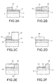
- FIGS. 2A to 2F illustrate a method of manufacturing a semiconductor-on-insulator substrate according to the present invention.
- the Figure 2A shows the structure 7 obtained above on which a first mask is in progress.
- a protective layer 8 made of silicon oxide, deposited for example by LPCVD and having a thickness of between 3 and 20 nm, is firstly formed, then a layer of silicon nitride, deposited for example by LPCVD. or PECVD and thickness between 50 and 500 nm.
- the silicon nitride layer is then photolithographed and then etched to obtain the pattern referenced 9 on the screen.
- Figure 2A shows the structure 7 obtained above on which a first mask is in progress.
- a protective layer 8 made of silicon oxide, deposited for example by LPCVD and having a thickness of between 3 and 20 nm, is firstly formed, then a layer of silicon nitride, deposited for example by LPCVD. or PECVD and thickness between 50 and 500 nm.
- the silicon nitride layer is then photolithographed and then etched to obtain the pattern referenced 9 on
- the silicon nitride pattern 9 exposes part of the layer 8 to silicon oxide.
- the exposed portion of the layer 8 is then removed, for example by wet etching (diluted HF), to leave a pattern 14 of silicon oxide.
- a layer 10 of SiGe stressed in tension and with a ⁇ 111> orientation is formed as the layer 3 (see FIG. Figure 2B ).
- the stress percentage of layer 10 depends on the parameter of surface mesh of the constrained silicon layer 3 and the composition of the SiGe layer 10. It is possible, for example, to deposit a layer of Si 0.9 Ge 0.1 on a substrate 7 of the type sSOI 20% (parameter of surface mesh equivalent to that of an alloy of Si 0.8 Ge 0.2 ). The equivalent voltage stress will then be equivalent to a mesh parameter mismatch of 0.4%.
- the high-temperature oxidation is then carried out, according to the germanium enrichment technique, to obtain a layer 11 of constrained germanium resting on the buried oxide layer 4.
- the layer 11 of constrained germanium is then covered with a layer 12 of silicon oxide (see Figure 2C ).
- the layer 10 of Si 1-x Ge x passes from a stress in tension to a stress in compression. Note that for x equal to the stress percentage of the initial sSOI, then the Si 1-x Ge x layer has no mechanical stress.
- a mixed substrate comprising, on the buried oxide layer 4, a strained silicon layer 13 in tension ⁇ 111> adjoining a layer 11 of germanium constrained in compression ⁇ 111>.
- the layers 11 and 13 are suitable for producing CMOS transistors: N-MOS transistors on the stressed silicon layer 13 and P-MOS on the constrained germanium layer 11.
- the silicon nitride pattern 9 and the silicon oxide pattern 14 are then removed, for example by means of wet etching: H 3 PO 4 for the nitride and HF for the oxide.
- the second mask After removing the first mask, we proceed to the formation of the second mask. For this purpose, a layer of silicon nitride, for example 50 nm thick, is formed. The silicon nitride layer is then photolithographed and then etched to obtain the pattern referenced 16 on the 2D figure . The silicon nitride pattern 16 exposes a portion of the layer 11 of constrained germanium.
- the epitaxy is carried out at low temperature (for example around 400 ° C) and the final thickness of the thick layer of germanium (for photonic components) is the order of a few hundred nm, ideally 400 nm.
- the formation of the germanium layer 18 leaves a constrained germanium layer 19 for the manufacture of MOS transistors.
- the layer 19 has a thickness less than 70 nm.
- the figure 2F shows the structure finally obtained and formed of a support 6 of silicon supporting a buried oxide layer 4 and a semiconductor-on-insulator layer consisting of adjacent parts: a thin layer 13 of constrained silicon, a thin layer 19 of constrained germanium and a relaxed thick layer 18 of germanium.
- the figure 3 represents a graph of the critical plastic relaxation thickness for an epitaxy of a silicon and germanium alloy as a function of the percentage of germanium in the alloy and as a function of the starting substrate.
- curve 31 represents the critical thickness curve of Si 1-x Ge x on unstressed silicon on insulator (SOI)
- curve 32 represents the critical thickness curve of Si 1-x Ge x on forced silicon.
- sSOI 20% represents the critical thickness curve of Si 1-x Ge x on Silicon constrained sSOI 35%
- curve 34 represents the critical thickness curve of Si 1-x Ge x on 50% sSOI-constrained silicon.
- the invention therefore makes it possible to provide substrates comprising a semiconductor-on-insulator layer comprising a sSOI ⁇ 111> zone for producing N-MOS transistors, a fine sGeOI zone ⁇ 111> for producing P-MOS transistors, and a GeOl area thick ⁇ 111> for the production of photodetectors.
- the epitaxial resumption carried out on the sGeOI area and dedicated to the photodetection can be a pure Ge epitaxial uptake or an alternation of n, p or unintentionally doped doped (nid) Ge deposits to achieve a PIN structure.
Landscapes
- Recrystallisation Techniques (AREA)
- Metal-Oxide And Bipolar Metal-Oxide Semiconductor Integrated Circuits (AREA)
- Thin Film Transistor (AREA)
Applications Claiming Priority (1)
| Application Number | Priority Date | Filing Date | Title |
|---|---|---|---|
| FR0756418A FR2918793B1 (fr) | 2007-07-11 | 2007-07-11 | Procede de fabrication d'un substrat semiconducteur-sur- isolant pour la microelectronique et l'optoelectronique. |
Publications (2)
| Publication Number | Publication Date |
|---|---|
| EP2015349A1 true EP2015349A1 (de) | 2009-01-14 |
| EP2015349B1 EP2015349B1 (de) | 2013-04-10 |
Family
ID=39092793
Family Applications (1)
| Application Number | Title | Priority Date | Filing Date |
|---|---|---|---|
| EP08159811.2A Ceased EP2015349B1 (de) | 2007-07-11 | 2008-07-07 | Verfahren zur Herstellung eines Halbleiter-Isolator-Schichtsystem-Substrats für die Mikroelektronik und Optoelektronik |
Country Status (4)
| Country | Link |
|---|---|
| US (1) | US7648893B2 (de) |
| EP (1) | EP2015349B1 (de) |
| JP (1) | JP5336118B2 (de) |
| FR (1) | FR2918793B1 (de) |
Families Citing this family (13)
| Publication number | Priority date | Publication date | Assignee | Title |
|---|---|---|---|---|
| DE102009035418B4 (de) * | 2009-07-31 | 2012-08-16 | Globalfoundries Dresden Module One Llc & Co. Kg | Herstellung einer Kanalhalbleiterlegierung durch Abscheiden einer Hartmaske für das selektive epitaktische Aufwachsen |
| US8211772B2 (en) * | 2009-12-23 | 2012-07-03 | Intel Corporation | Two-dimensional condensation for uniaxially strained semiconductor fins |
| WO2011121776A1 (ja) * | 2010-03-31 | 2011-10-06 | 株式会社 東芝 | 半導体装置の製造方法 |
| KR101699313B1 (ko) * | 2010-10-05 | 2017-02-13 | 엘지전자 주식회사 | 태양 전지 제조 방법 |
| US8298923B2 (en) * | 2010-10-27 | 2012-10-30 | International Business Machinces Corporation | Germanium-containing release layer for transfer of a silicon layer to a substrate |
| US8731017B2 (en) | 2011-08-12 | 2014-05-20 | Acorn Technologies, Inc. | Tensile strained semiconductor photon emission and detection devices and integrated photonics system |
| DE102014205364A1 (de) * | 2014-03-21 | 2015-09-24 | Ihp Gmbh - Innovations For High Performance Microelectronics / Leibniz-Institut Für Innovative Mikroelektronik | Herstellung von Halbleiter-auf-Isolator-Schichtstrukturen |
| US9472575B2 (en) * | 2015-02-06 | 2016-10-18 | International Business Machines Corporation | Formation of strained fins in a finFET device |
| US11192788B2 (en) | 2017-02-24 | 2021-12-07 | National University Of Singapore | Two-dimensional amorphous carbon coating and methods of growing and differentiating stem cells |
| FR3068508B1 (fr) * | 2017-06-30 | 2019-07-26 | Soitec | Procede de transfert d'une couche mince sur un substrat support presentant des coefficients de dilatation thermique differents |
| CN108511395B (zh) * | 2018-03-30 | 2021-04-02 | 上海华力微电子有限公司 | 一种具有双极应力的绝缘体上硅结构及其制造方法 |
| KR20220167795A (ko) | 2020-03-10 | 2022-12-21 | 내셔널 유니버시티 오브 싱가포르 | 씨드층, 씨드층을 포함하는 헤테로구조물, 및 씨드층을 사용하여 재료 층을 형성하는 방법 |
| EP3965141A1 (de) * | 2020-09-04 | 2022-03-09 | Siltronic AG | Verfahren zur abscheidung einer silizium-germanium-schicht auf einem substrat |
Citations (3)
| Publication number | Priority date | Publication date | Assignee | Title |
|---|---|---|---|---|
| FR2681472A1 (fr) | 1991-09-18 | 1993-03-19 | Commissariat Energie Atomique | Procede de fabrication de films minces de materiau semiconducteur. |
| US20050116290A1 (en) * | 2003-12-02 | 2005-06-02 | De Souza Joel P. | Planar substrate with selected semiconductor crystal orientations formed by localized amorphization and recrystallization of stacked template layers |
| US20060157706A1 (en) * | 2005-01-18 | 2006-07-20 | International Business Machines Corporation | Structure and method for manufacturing strained silicon directly-on-insulator substrate with hybrid crystalline orientation and different stress levels |
Family Cites Families (9)
| Publication number | Priority date | Publication date | Assignee | Title |
|---|---|---|---|---|
| JP3607194B2 (ja) * | 1999-11-26 | 2005-01-05 | 株式会社東芝 | 半導体装置、半導体装置の製造方法、及び半導体基板 |
| FR2870043B1 (fr) * | 2004-05-07 | 2006-11-24 | Commissariat Energie Atomique | Fabrication de zones actives de natures differentes directement sur isolant et application au transistor mos a simple ou double grille |
| JP4604637B2 (ja) * | 2004-10-07 | 2011-01-05 | ソニー株式会社 | 半導体装置および半導体装置の製造方法 |
| JP4617820B2 (ja) * | 2004-10-20 | 2011-01-26 | 信越半導体株式会社 | 半導体ウェーハの製造方法 |
| CN100481345C (zh) * | 2005-02-24 | 2009-04-22 | 硅绝缘体技术有限公司 | SiGe层的热氧化及其应用 |
| CN101268547B (zh) * | 2005-07-26 | 2014-07-09 | 琥珀波系统公司 | 包含交替有源区材料的结构及其形成方法 |
| EP1763069B1 (de) * | 2005-09-07 | 2016-04-13 | Soitec | Herstellungsverfahren einer Heterostruktur |
| JP2007142291A (ja) * | 2005-11-21 | 2007-06-07 | Canon Anelva Corp | 半導体構造およびその成長方法 |
| JP4310399B2 (ja) * | 2006-12-08 | 2009-08-05 | 株式会社東芝 | 半導体装置及びその製造方法 |
-
2007
- 2007-07-11 FR FR0756418A patent/FR2918793B1/fr not_active Expired - Fee Related
-
2008
- 2008-06-24 US US12/144,992 patent/US7648893B2/en active Active
- 2008-07-07 EP EP08159811.2A patent/EP2015349B1/de not_active Ceased
- 2008-07-10 JP JP2008180386A patent/JP5336118B2/ja not_active Expired - Fee Related
Patent Citations (4)
| Publication number | Priority date | Publication date | Assignee | Title |
|---|---|---|---|---|
| FR2681472A1 (fr) | 1991-09-18 | 1993-03-19 | Commissariat Energie Atomique | Procede de fabrication de films minces de materiau semiconducteur. |
| US5374564A (en) | 1991-09-18 | 1994-12-20 | Commissariat A L'energie Atomique | Process for the production of thin semiconductor material films |
| US20050116290A1 (en) * | 2003-12-02 | 2005-06-02 | De Souza Joel P. | Planar substrate with selected semiconductor crystal orientations formed by localized amorphization and recrystallization of stacked template layers |
| US20060157706A1 (en) * | 2005-01-18 | 2006-07-20 | International Business Machines Corporation | Structure and method for manufacturing strained silicon directly-on-insulator substrate with hybrid crystalline orientation and different stress levels |
Non-Patent Citations (1)
| Title |
|---|
| T. TEZUKA ET AL.: "Ultra-thin body SiGe-on-Insulator p-MOSFETs with high mobility SiGe surface channels", EDL 2002, vol. 50, no. 5, 2003, pages 1328 - 1333 |
Also Published As
| Publication number | Publication date |
|---|---|
| US20090017602A1 (en) | 2009-01-15 |
| FR2918793A1 (fr) | 2009-01-16 |
| JP5336118B2 (ja) | 2013-11-06 |
| EP2015349B1 (de) | 2013-04-10 |
| US7648893B2 (en) | 2010-01-19 |
| JP2009027163A (ja) | 2009-02-05 |
| FR2918793B1 (fr) | 2009-10-09 |
Similar Documents
| Publication | Publication Date | Title |
|---|---|---|
| EP2015349B1 (de) | Verfahren zur Herstellung eines Halbleiter-Isolator-Schichtsystem-Substrats für die Mikroelektronik und Optoelektronik | |
| EP2296180B1 (de) | Verfahren zur Stabilisation von Nanodrähten aus Germanium erhalten durch Kondensation | |
| EP2157603B1 (de) | Verfahren zur Herstellung von lokalisierten GeOI-Strukturen, die durch Germanium-Anreicherung erhalten werden | |
| FR2845523A1 (fr) | Procede pour realiser un substrat par transfert d'une plaquette donneuse comportant des especes etrangeres, et plaquette donneuse associee | |
| WO2002037556A1 (fr) | Procede de fabrication d'une structure empilee comprenant une couche mince adherant a un substrat cible | |
| EP1830401B1 (de) | Mikrostruktur zur Bildung eines Substrats aus Silizium und Germanium auf einem Isolator und vom Typ Si1-XGeX | |
| EP2075826A2 (de) | Verfahren zur Herstellung eines Halbleiter-auf-Isolator-Substrats, das eine Anreicherungsetappe mit lokalisiertem Germanium umfasst | |
| FR2938120A1 (fr) | Procede de formation d'une couche monocristalline dans le domaine micro-electronique | |
| EP1922752B1 (de) | Verfahren zum transfer eines dünnfilms auf einen träger | |
| EP1968103B1 (de) | Verfahren zur Herstellung eines Mischsubstrats und Verwendung für die Herstellung von CMOS-Schaltungen | |
| FR2774511A1 (fr) | Substrat compliant en particulier pour un depot par hetero-epitaxie | |
| FR3051596A1 (fr) | Procede de fabrication d'un substrat de type semi-conducteur contraint sur isolant | |
| FR2933534A1 (fr) | Procede de fabrication d'une structure comprenant une couche de germanium sur un substrat | |
| EP1938362B1 (de) | Verfahren zum herstellen eines dünnfilmelements | |
| EP1830400A1 (de) | Verfahren zur Herstellung eines Substrats durch Germaniumkondensation | |
| EP3504729B1 (de) | Verfahren zur herstellung einer verspannten schicht auf der basis von germanium-zinn | |
| EP1580805B1 (de) | Verfahren zum Präparieren einer Siliziumoxidschicht durch Oxidation bei hohe Temperatur auf einem Substrat mit einer Silizium-Germanium Oberfläche | |
| FR2860340A1 (fr) | Collage indirect avec disparition de la couche de collage | |
| FR2977075A1 (fr) | Procede de fabrication d'un substrat semi-conducteur, et substrat semi-conducteur | |
| WO2005001915A2 (fr) | Procede de realisation d'une structure empilee par transfert de couche mince | |
| EP3903341B1 (de) | Verfahren zur herstellung eines substrats für einen vorderseitigen bildsensor | |
| EP4606194A1 (de) | Verfahren zur herstellung einer piezoelektrischen schicht auf einem substrat | |
| EP3018697A1 (de) | Verfahren zur bestimmung der gewünschten aufbringungsparameter für eine dünnschicht aus iii-v-halbleitermaterial | |
| FR2883661A1 (fr) | Transistor a effet de champ multi-grille a canal multi-couche | |
| FR2886457A1 (fr) | Procede de fabrication d'une structure a couche d'oxyde d'epaisseur desiree,notammentt sur substrat de ge ou sige |
Legal Events
| Date | Code | Title | Description |
|---|---|---|---|
| PUAI | Public reference made under article 153(3) epc to a published international application that has entered the european phase |
Free format text: ORIGINAL CODE: 0009012 |
|
| AK | Designated contracting states |
Kind code of ref document: A1 Designated state(s): AT BE BG CH CY CZ DE DK EE ES FI FR GB GR HR HU IE IS IT LI LT LU LV MC MT NL NO PL PT RO SE SI SK TR |
|
| AX | Request for extension of the european patent |
Extension state: AL BA MK RS |
|
| 17P | Request for examination filed |
Effective date: 20090706 |
|
| AKX | Designation fees paid |
Designated state(s): DE FR GB IT |
|
| RAP1 | Party data changed (applicant data changed or rights of an application transferred) |
Owner name: COMMISSARIAT A L'ENERGIE ATOMIQUE ET AUX ENERGIES |
|
| REG | Reference to a national code |
Ref country code: DE Ref legal event code: R079 Ref document number: 602008023626 Country of ref document: DE Free format text: PREVIOUS MAIN CLASS: H01L0021200000 Ipc: H01L0021020000 |
|
| RIC1 | Information provided on ipc code assigned before grant |
Ipc: H01L 21/02 20060101AFI20120726BHEP |
|
| GRAP | Despatch of communication of intention to grant a patent |
Free format text: ORIGINAL CODE: EPIDOSNIGR1 |
|
| GRAS | Grant fee paid |
Free format text: ORIGINAL CODE: EPIDOSNIGR3 |
|
| GRAA | (expected) grant |
Free format text: ORIGINAL CODE: 0009210 |
|
| AK | Designated contracting states |
Kind code of ref document: B1 Designated state(s): DE FR GB IT |
|
| REG | Reference to a national code |
Ref country code: GB Ref legal event code: FG4D Free format text: NOT ENGLISH |
|
| REG | Reference to a national code |
Ref country code: DE Ref legal event code: R096 Ref document number: 602008023626 Country of ref document: DE Effective date: 20130606 |
|
| PLBE | No opposition filed within time limit |
Free format text: ORIGINAL CODE: 0009261 |
|
| STAA | Information on the status of an ep patent application or granted ep patent |
Free format text: STATUS: NO OPPOSITION FILED WITHIN TIME LIMIT |
|
| PG25 | Lapsed in a contracting state [announced via postgrant information from national office to epo] |
Ref country code: IT Free format text: LAPSE BECAUSE OF FAILURE TO SUBMIT A TRANSLATION OF THE DESCRIPTION OR TO PAY THE FEE WITHIN THE PRESCRIBED TIME-LIMIT Effective date: 20130410 |
|
| 26N | No opposition filed |
Effective date: 20140113 |
|
| REG | Reference to a national code |
Ref country code: DE Ref legal event code: R097 Ref document number: 602008023626 Country of ref document: DE Effective date: 20140113 |
|
| PGFP | Annual fee paid to national office [announced via postgrant information from national office to epo] |
Ref country code: DE Payment date: 20140711 Year of fee payment: 7 |
|
| PGFP | Annual fee paid to national office [announced via postgrant information from national office to epo] |
Ref country code: GB Payment date: 20140717 Year of fee payment: 7 |
|
| REG | Reference to a national code |
Ref country code: DE Ref legal event code: R119 Ref document number: 602008023626 Country of ref document: DE |
|
| GBPC | Gb: european patent ceased through non-payment of renewal fee |
Effective date: 20150707 |
|
| PG25 | Lapsed in a contracting state [announced via postgrant information from national office to epo] |
Ref country code: DE Free format text: LAPSE BECAUSE OF NON-PAYMENT OF DUE FEES Effective date: 20160202 Ref country code: GB Free format text: LAPSE BECAUSE OF NON-PAYMENT OF DUE FEES Effective date: 20150707 |
|
| REG | Reference to a national code |
Ref country code: FR Ref legal event code: PLFP Year of fee payment: 9 |
|
| REG | Reference to a national code |
Ref country code: FR Ref legal event code: PLFP Year of fee payment: 10 |
|
| REG | Reference to a national code |
Ref country code: FR Ref legal event code: PLFP Year of fee payment: 11 |
|
| PGFP | Annual fee paid to national office [announced via postgrant information from national office to epo] |
Ref country code: FR Payment date: 20230724 Year of fee payment: 16 |
|
| PG25 | Lapsed in a contracting state [announced via postgrant information from national office to epo] |
Ref country code: FR Free format text: LAPSE BECAUSE OF NON-PAYMENT OF DUE FEES Effective date: 20240731 |