EP2015453A2 - Treiberschaltung für ein spannungsgesteuertes elektronisches Bauteil - Google Patents
Treiberschaltung für ein spannungsgesteuertes elektronisches Bauteil Download PDFInfo
- Publication number
- EP2015453A2 EP2015453A2 EP08157839A EP08157839A EP2015453A2 EP 2015453 A2 EP2015453 A2 EP 2015453A2 EP 08157839 A EP08157839 A EP 08157839A EP 08157839 A EP08157839 A EP 08157839A EP 2015453 A2 EP2015453 A2 EP 2015453A2
- Authority
- EP
- European Patent Office
- Prior art keywords
- terminal
- gate
- resistor
- drive circuit
- emitter
- Prior art date
- Legal status (The legal status is an assumption and is not a legal conclusion. Google has not performed a legal analysis and makes no representation as to the accuracy of the status listed.)
- Granted
Links
Images


Classifications
-
- H—ELECTRICITY
- H03—ELECTRONIC CIRCUITRY
- H03K—PULSE TECHNIQUE
- H03K17/00—Electronic switching or gating, i.e. not by contact-making and –breaking
- H03K17/04—Modifications for accelerating switching
- H03K17/0406—Modifications for accelerating switching in composite switches
-
- H—ELECTRICITY
- H03—ELECTRONIC CIRCUITRY
- H03K—PULSE TECHNIQUE
- H03K17/00—Electronic switching or gating, i.e. not by contact-making and –breaking
- H03K17/16—Modifications for eliminating interference voltages or currents
- H03K17/168—Modifications for eliminating interference voltages or currents in composite switches
-
- H—ELECTRICITY
- H03—ELECTRONIC CIRCUITRY
- H03K—PULSE TECHNIQUE
- H03K17/00—Electronic switching or gating, i.e. not by contact-making and –breaking
- H03K17/04—Modifications for accelerating switching
- H03K17/041—Modifications for accelerating switching without feedback from the output circuit to the control circuit
- H03K17/0412—Modifications for accelerating switching without feedback from the output circuit to the control circuit by measures taken in the control circuit
- H03K17/04123—Modifications for accelerating switching without feedback from the output circuit to the control circuit by measures taken in the control circuit in field-effect transistor switches
-
- H—ELECTRICITY
- H03—ELECTRONIC CIRCUITRY
- H03K—PULSE TECHNIQUE
- H03K17/00—Electronic switching or gating, i.e. not by contact-making and –breaking
- H03K17/16—Modifications for eliminating interference voltages or currents
- H03K17/161—Modifications for eliminating interference voltages or currents in field-effect transistor switches
- H03K17/162—Modifications for eliminating interference voltages or currents in field-effect transistor switches without feedback from the output circuit to the control circuit
Definitions
- the present invention relates to a drive circuit for a voltage driven element and particularly, but not exclusively, to a drive circuit for driving a voltage-driven-type element adapted to be used for a switching circuit, an inverter circuit or the like provided in a unit such as an electric vehicle that needs high electric power.
- aspects of the invention relate to a drive circuit, to a voltage driven element, to a method, to an apparatus and to a vehicle.
- a voltage driven type element such as an insulated gate bipolar transistor (IGBT) has been used in a switching circuit or an inverter circuit employed in power control circuits for applications requiring high power.
- Japanese Patent Application Publication No. 2003-125574 discloses a switching circuit and inverter circuit that includes two series-connected IGBTs where each is connected with a freewheeling diode (FWD) in the form of an inverse-parallel connection.
- a reactor functioning as an inductive load is connected to the connection point of the IGBTs.
- the first IGBT (IGBT1) is connected to a direct-current voltage
- the second IGBT (IGBT2) is connected to ground (GND)
- a gate terminal of each IGBT is connected to a drive circuit.
- This drive circuit includes a push-pull transistor for charging/discharging the IGBT by means of an input of gate signal, a gate resistor connected between this transistor and the gate terminal of the IGBT, and an external capacitor connected between an emitter terminal of the IGBT and the gate resistor.
- an external capacitor injects electric charge to a gate-emitter capacitor whereby the external capacitor is located between the gate terminal and the emitter terminal of the IGBT2.
- the reduction of gate voltage is prevented, and the reduction of the gate charging speed is suppressed.
- a current amplification factor is not enlarged, a recovery current of the FWD is suppressed.
- the rate of decrease of the collector-emitter voltage is suppressed, and the loss during a reverse-transfer-capacitance charging process is reduced so that the reduction of a turn-on loss is achieved.
- Embodiments of the invention may provide a drive circuit for driving a voltage-driven element that is capable of reducing the turn-on loss without enlarging a capacitor even when the gate-collector capacitor is large.
- a drive circuit for driving a voltage-driven element including a gate terminal, an emitter terminal and a collector terminal
- the drive circuit comprising a first semiconductor switching element including an output terminal disposed between a power source for the drive circuit and the gate terminal, a first resistor disposed between the output terminal and the gate terminal and a capacitive element connected in parallel with the first semiconductor element and configured to supply an electric charge from the power source to a portion between the gate terminal and the emitter terminal after an electric charge accumulated in the portion between the gate terminal and the emitter terminal is supplied to a portion between the gate terminal and the collector terminal.
- the capacitive element comprises a first conductor, a second conductor and an insulator provided between the first conductor and the second conductor.
- the first conductor is connected between the power source and the first semiconductor switching element and the second conductor is connected between the first resistor and the gate terminal.
- the drive circuit may comprise a second semiconductor switching element complementary to the first semiconductor switching element and a second resistor, the second semiconductor switching element and the second resistor disposed between the first resistor, the gate terminal and the emitter terminal.
- the second resistor is connected in series between the first resistor and a junction of the second conductor and the gate terminal; and the second semiconductor switching element is coupled between the emitter terminal and a junction of the first resistor and the second resistor.
- the second resistor is connected between a first terminal of the second semiconductor switching element and a junction of the first resistor, the second conductor and the gate terminal; and a second terminal of the second semiconductor switching element is coupled to the emitter terminal.
- the first conductor is connected between the power source and the first semiconductor switching element and the second conductor is connected between the output terminal and the first resistor.
- the drive circuit may comprise a second semiconductor switching element complementary to the first semiconductor switching element and a second resistor coupled between the output terminal and a first terminal of the second semiconductor switching element, a second terminal of the second semiconductor switching element connected to the emitter terminal.
- the capacitive element includes a semiconductor component including an anode and a cathode.
- the cathode is connected between the power source and the first semiconductor switching element and the anode is connected between the first resistor and the gate terminal.
- the cathode is connected between the power source and the first semiconductor switching element and the anode is connected between the output terminal and the first resistor.
- the drive circuit may comprise a second semiconductor switching element complementary to the first semiconductor switching element and a second resistor, the second semiconductor switching element and the second resistor disposed among the first resistor, the capacitive element, and the emitter terminal.
- the drive circuit comprises a plurality of resistor elements between the output terminal and the gate terminal, at least one of the plurality of resistor elements configured as a current-limiting resistor.
- a drive circuit for driving a voltage-driven element including a gate terminal, an emitter terminal and a collector terminal
- the drive circuit comprising first means for switching from an on conduction state to an off conduction state and including an output terminal, means for connecting the first means for switching between a power source for the drive circuit and the gate terminal, a first resistor, means for connecting the first resistor between the output terminal and the gate terminal, capacitive means for supplying an electric charge from the power source to a portion between the gate terminal and the emitter terminal after an electric charge accumulated in the portion between the gate terminal and the emitter terminal is supplied to a portion between the gate terminal and the collector terminal due to switching of the first means for switching and means for connecting the capacitive means in parallel with the first means for switching.
- a method for driving a voltage-driven element including a gate terminal, an emitter terminal and a collector terminal
- the drive method comprising supplying electric power to the voltage-driven element using a first semiconductor switching element disposed between the gate terminal and a power source and a resistor disposed between the output terminal of the first semiconductor switching element and the gate terminal and supplying an electric charge from the power source through a capacitive element in parallel with the first semiconductor switching element to a portion between the gate terminal and the emitter terminal after supplying an electric charge accumulated in the portion between the gate terminal and the emitter terminal to a portion between the gate terminal and the collector terminal.
- a drive circuit for driving a voltage-driven element including a gate terminal, an emitter terminal and a collector terminal may comprise a first semiconductor switching element including an output terminal disposed between a power source for the drive circuit and the gate terminal, a first resistor disposed between the output terminal and the gate terminal and a capacitive element connected in parallel with the first semiconductor element and configured to supply an electric charge from the power source to a portion between the gate terminal and the emitter terminal after an electric charge accumulated in the portion between the gate terminal and the emitter terminal is supplied to a portion between the gate terminal and the collector terminal.
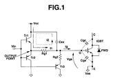
- FIG. 1 illustrates a first embodiment of the drive circuit.
- the drive circuit is connected to a voltage-driven-type element adapted to be used for a switching circuit, an inverter circuit or the like.
- the voltage-driven-type element may be an insulated gate bipolar transistor (IGBT), a MOSFET, a MOS thyristor or the like and is not limited to what is shown in the drawing figures.
- the voltage driven-type element is an IGBT.
- the drive circuit is connected to a gate terminal G of the IGBT.
- the IGBT is connected with a freewheeling diode (FWD) in the form of an inverse-parallel connection (back-to-back connection).
- FWD freewheeling diode
- Gate-emitter capacitance Cge exists between gate terminal G of the IGBT and an emitter terminal E of the IGBT, and gate-collector capacitance Cgc exists between gate terminal G and a collector terminal C.
- a reference electric potential Vee is applied to emitter terminal E.
- the drive circuit according to the first embodiment includes a transistor Tr1 and a transistor Tr2 complementary to the transistor Tr1 and connected by their emitters at a common junction (shown as "output point" on FIG. 1 ).
- a gate resistor Rg1 is connected between the output point and gate terminal G of the IGBT and a condenser Cex.
- Condenser Cex includes a first conductor connected with a power source Vcc for the drive circuit at the collector terminal of transistor Tr1, a second conductor connected to a point between gate resistor Rg1 and gate terminal G and an insulator between the first conductor and the second conductor.
- Transistor Tr1 and transistor Tr2 form or define push-pull transistors for performing charging and discharging of the IGBT in accordance with an input of a gate signal Vin.
- a transistor Tr3 and a current-limiting resistor Rg2 are connected between emitter terminal E and the point between gate resistor Rg1 and gate terminal G. More specifically, current-limiting resistor Rg2 is connected between the point between gate resistor Rg1 and gate terminal G and the emitter of transistor Tr3, which is in turn connected by its collector terminal to emitter terminal E through their common connection to reference potential Vee.
- Transistor Tr3 functions as a semiconductor element complementary to transistor Tr1. Gate (or base) terminals of transistor Tr1, transistor Tr2 and transistor Tr3 are connected to gate signal Vin.
- transistor Tr1 is a NPN transistor
- transistors Tr2 and Tr3 are PNP transistors.
- gate signal Vin changes from LO level to Hl level
- transistor Tr1 makes a state transition from OFF to ON
- transistors Tr2 and Tr3, used for discharging the gate electric charge make a state transition from ON to OFF.
- a gate charging current i1 flows from power source Vcc to gate-emitter capacitance Cge so that gate-emitter capacitance Cge (a capacitor equivalent between the gate and emitter terminals) is charged.
- the electric charge accumulated in condenser Cex is discharged through transistor Tr1 and gate resistor Rg1 to gate-emitter capacitance Cge in the same direction as shown by current i2 in FIG. 1 .
- gate voltage Vge rises.
- the IGBT starts to transition to the ON state
- a collector-emitter voltage Vce (voltage between the collector C and emitter E terminals) starts to decrease.
- a collector current Ic of the IGBT increases as shown in FIG. 2 . Then, when collector current Ic reaches a predetermined value, charging to gate-collector capacitance Cgc of the IGBT starts. At this time, the electric charge accumulated in gate-emitter capacitance Cge is discharged to gate-collector capacitance Cgc.
- This decrease in the electric charge of gate-emitter capacitance Cge serves to reduce gate voltage Vge.
- gate-emitter capacitance Cge is transiently charged by power source Vcc through condenser Cex by using a bypass of gate resistor Rg1 and final-stage transistor Tr1.
- gate voltage Vge is suppressed.
- collector-emitter voltage Vce is reduced so that the IGBT makes the state transition from OFF to ON.
- FIG. 2 is a time chart of the circuit configuration diagram shown in FIG. 1 .
- time point t1 represents when gate signal Vin changes from HI level to LO level
- time point t2 represents when gate signal Vin changes from LO level to HI level
- time point t3 represents when collector-emitter voltage Vce begins to decrease
- time point t6 represents when gate-collector capacitance Cgc starts to charge
- Time point t4 represents when the drop of collector-emitter voltage Vce ends
- time point t5 represents when gate voltage Vge starts to rise further after gate voltage Vge has been stabilized.
- a time period between time point t2 and time point t6 represents an initial charging process
- a time period after time point t6 represents a reverse-transfer-capacitance charging process.
- the initial charging process means the time period when the gate signal becomes HI and allows for the start of charging gate-emitter capacitance Cge of the IGBT. Then, collector-emitter voltage Vce of the IGBT starts to drop in response to gate voltage Vge brought in excess of its threshold value, and collector current Ic of the IGBT increases according to this drop so that the charging of gate-collector capacitance Cgc of the IGBT begins. Namely, the beginning and ending of the above events define the period of the initial charging process.
- the reverse-transfer-capacitance charging process means the time period when collector current Ic reaches its maximum value after the initial charging process (i.e., after starting to charge gate-collector capacitance Cgc, which is a reverse transfer capacitance), and then the charging for gate-collector capacitance Cgc and gate-emitter capacitance Cge finishes. Namely, the beginning and ending of the above events define the period of the reverse-transfer-capacitance charging process.
- transistors Tr2 and Tr3 change from an OFF state to an ON state.
- the electric charge of gate-emitter capacitance Cge and the electric charge of gate-collector capacitance Cgc are discharged through transistor Tr3 and current-limiting resistor Rg2.
- a gate charging current ig has negative values.
- the IGBT changes its state from ON to OFF in response to the reduction of gate voltage Vge. Namely, collector-emitter voltage Vce increases, collector current Ic decreases to 0A, and the IGBT is turned off.
- transistor Tr1 changes its state from OFF to ON, as mentioned previously. Accordingly, gate charging current i1 starts to flow from power source Vcc to gate-emitter capacitance Cge, and discharging current i2 starts to flow from condenser Cex to gate-emitter capacitance Cge in the direction of arrow shown in FIG. 1 . Accordingly, gate voltage Vge starts to rise. Afterward, at time point t3, gate voltage Vge rises above a threshold value so that the IGBT makes the state transition from OFF to ON. Namely, collector-emitter voltage Vce starts to drop, and collector current Ic of the IGBT starts to rise. As shown in FIG. 2 , gate voltage Vge continues to rise until time point t6.
- Equation (4) gives the value of gate voltage Vge just after time point t6 and shows that gate-emitter capacitance Cge is charged with impedance Z(Cex) from power source Vcc through condenser Cex by using the bypass of gate resistor Rg1 and transistor Tr1 instantaneously after the electric charge accumulated in gate-emitter capacitance Cge is discharged to gate-collector capacitance Cgc.
- ⁇ Vge(t) shown in equation (3) is a voltage rising amount because of the bypass current that flows from power source Vcc through condenser Cex to gate-emitter capacitance Cge by passing the bypass of gate resistor Rg1 and final-stage transistor Tr1 in order to charge gate-emitter capacitance Cge.
- gate-emitter capacitance Cge In the case of earlier technology such as that described initially, an impedance of transistor Tr1 and gate resistor Rg1 is higher than an impedance of gate-emitter capacitance Cge. Hence, power source Vcc cannot efficiently charge gate-collector capacitance Cgc, which means that gate charging current ig decreases during the period between time points t6 and t4 (dotted line). Meanwhile, the electric charge accumulated in gate-emitter capacitance Cge up to just before time point t6 is discharged to gate-collector capacitance Cgc. Moreover, the electric charge accumulated in condenser Cex up to just before time point t6 is discharged to gate-emitter capacitance Cge and gate-collector capacitance Cgc. Therefore, in the earlier technology, gate voltage Vge is reduced during the period between time points t6 and t4 (dotted line).
- Vge ⁇ 0 ⁇ ⁇ Cex + Cge / ( Cex + Cge + Cgc ) * Vge ( t ⁇ 6 ) ⁇ ; wherein Vge(t6)' represents a value of gate voltage Vge just before time point t6 in the earlier technology.
- gate voltage Vge solid line
- Vge dotted line
- the earlier technology appears to suppress the decrease in gate voltage Vge if only equations (2) and (5) are compared.
- the decrease of gate voltage Vge is greatly suppressed by the effect of equation (3). Accordingly, as shown by gate charging current ig (solid line) between time points t6 and t4 in FIG. 2 , gate charging current ig (solid line) according to the teachings herein is larger than that in the earlier technology.
- gate charging current ig is larger than gate charging current of the earlier technology is because bypass current flows from power source Vcc through condenser Cex, bypassing transistor Tr1 and gate resistor Rg1, in order to charge gate-emitter capacitance Cge. As shown by ⁇ Vge(t) in equation (3), a voltage rising amount produced by this bypass current allows gate voltage Vge to drop less than the earlier technology.
- gate voltage Vge increases more than that of earlier technology because of the effect of voltage rising amount ⁇ Vge(t) shown in equation (3) in response to the variation of gate-collector capacitance Cgc.
- gate voltage Vge is reduced during the charging time period (from t6 to t4) of gate-collector capacitance Cgc because the electric charge accumulated in gate-emitter capacitance Cge is discharged to gate-collector capacitance Cgc.
- gate-emitter capacitance Cge is transiently charged from power source Vcc through condenser Cex by using the bypass of gate resistor Rg1 and transistor Tr1, so that the reduction of gate voltage Vge can be suppressed. Therefore, the reduction of a gate charging speed, namely the lessening of a dropping speed of collector-emitter voltage Vce caused by the reduction of gate voltage Vge during the charging of gate-collector capacitance Cgc, can be suppressed. Hence, a loss during the reverse-transfer-capacitance charging process can be further reduced, and a turn-on loss can be further reduced.
- FIG. 3 A drive circuit for driving a voltage-driven-type element according to a second embodiment is shown in FIG. 3 .
- the drive circuit of the present embodiment is similar to the drive circuit of the first embodiment so duplicative descriptions are omitted.
- the drive circuit according to the second embodiment includes transistor Tr1, transistor Tr2, gate resistor Rg1 connected between the output point (emitter) of transistor Tr1 and gate terminal G of the IGBT, a FWD connected to the IGBT in the form of an inverse-parallel connection, a current-limiting resistor Rg3 connected between transistor Tr1 and transistor Tr2, and condenser Cex.
- Gate terminals of transistor Tr1 and transistor Tr2 are connected to gate signal Vin.
- Power source Vcc is applied to the collector terminal of transistor Tr1, and reference potential Vee is applied to the collector terminal of transistor Tr2.
- One side of condenser Cex is connected with power source Vcc, and the other side of condenser Cex is connected between gate resistor Rg1 and the emitter of transistor Tr1.
- Current-limiting resistor Rg3 is connected between the emitters of transistor Tr1 and transistor Tr2, and gate resistor Rg1 is connected with condenser Cex at the output point (emitter) of transistor Tr1.
- gate-emitter capacitance Cge and gate-collector capacitance Cgc are discharged through transistor Tr2, gate resistor Rg1 and current-limiting resistor Rg3 by changing the state of transistor Tr2 from OFF to ON.
- gate-collector capacitance Cgc when charging gate-collector capacitance Cgc, the electric charge accumulated in gate-emitter capacitance Cge is discharged to gate-collector capacitance Cgc so that gate voltage Vge is reduced.
- gate-emitter capacitance Cge is transiently charged from power source Vcc through condenser Cex and gate resistor Rg1 by using the bypass of transistor Tr1. Therefore, drive circuit of the second embodiment can obtain similar results as in the first embodiment
- a drive circuit for driving a voltage-driven-type element according to a third embodiment is shown in FIG. 4 .
- the drive circuit of the present embodiment is similar to the drive circuit of the first embodiment so duplicative descriptions are omitted.
- the drive circuit according to the third embodiment includes transistor Tr1.
- gate resistor Rg1 and a current-limiting resistor Rg4 are connected in series between the output point (emitter) of transistor Tr1 and gate terminal G of the IGBT.
- a FWD is connected to the IGBT in the form of an inverse-parallel connection.
- a transistor Tr3 is connected between emitter terminal E of the IGBT and a connection point between gate resistor Rg1 and current-limiting resistor Rg4.
- the third embodiment also includes transistor Tr2 and condenser Cex. Gate terminals of transistor Tr1, transistor Tr2 and transistor Tr3 are connected to gate signal Vin.
- Power source Vcc is applied to the collector terminal of transistor Tr1, and reference potential Vee is applied to the collector terminals of transistor Tr2 and transistor Tr3, in addition to the emitter terminal E of the IGBT.
- One side of condenser Cex is connected with power source Vcc at the collector of transistor Tr1, and the other side of condenser Cex is connected between current-limiting resistor Rg4 and gate terminal G.
- Current-limiting resistor Rg4 is connected between a common junction of gate resistor Rg1 and the emitter of transistor Tr3 and gate terminal G.
- gate-emitter capacitance Cge and gate-collector capacitance Cgc is discharged through transistor Tr3 and current-limiting resistor Rg4 by changing the state of transistor Tr3 from OFF to ON.
- the electric charge accumulated in gate-emitter capacitance Cge is discharged to gate-collector capacitance Cgc so that gate voltage Vge is reduced.
- gate-emitter capacitance Cge is transiently charged from power source Vcc through condenser Cex by using the bypass of transistor Tr1, gate resistor Rg1 and current-limiting resistor Rg4. Therefore, drive circuit of the third embodiment can obtain similar results as in the first embodiment
- a drive circuit for driving a voltage-driven-type element according to a fourth embodiment is shown in FIG. 5 .
- the drive circuit of the present embodiment is similar to the drive circuit of the first embodiment so duplicative descriptions are omitted.
- the drive circuit according to the fourth embodiment includes transistor Tr1, gate resistor Rg1 connected between the output point (emitter) of transistor Tr1 and gate terminal G of the IGBT and a FWD connected to the IGBT in the form of an inverse-parallel connection.
- a transistor Tr3 and current-limiting resistor Rg2 are connected between emitter terminal E and a point between gate resistor Rg1 and gate terminal G.
- the fourth embodiment also includes a transistor Tr2 and a diode D. Gate terminals of transistor Tr1, transistor Tr2 and transistor Tr3 are connected to gate signal Vin. Power source Vcc is applied to the collector terminal of transistor Tr1, and reference potential Vee is applied to the collector terminals of transistor Tr2 and transistor Tr3, in addition to the emitter terminal E of the IGBT.
- diode D is connected with power source Vcc, and the anode of diode D is coupled to a common junction of current-limiting resistor Rg2, gate resistor Rg1 and gate terminal G.
- diode D is provided instead of condenser Cex.
- gate-emitter capacitance Cge when charging gate-collector capacitance Cgc, the electric charge accumulated in gate-emitter capacitance Cge is discharged to gate-collector capacitance Cgc so that gate voltage Vge is reduced.
- gate-emitter capacitance Cge is transiently charged from power source Vcc through a depletion capacitance of diode D by using the bypass of transistor Tr1 and gate resistor Rg1. Therefore, drive circuit of the fourth embodiment can obtain similar results as in the first embodiment.
- one gate resistor Rg1 is provided in the drive circuit for driving a voltage-driven-type element in each of the first to fourth embodiments.
- the number of gate resistors Rg1 is not limited to one, and a plurality of gate resistors Rg1 may be provided.
- condenser Cex of the drive circuit in the first embodiment is replaced with diode D.
- replacing capacitor Cex within diode D is not limited to the fourth embodiment, and it is within the scope of the invention to provide, a circuit configuration in which condenser Cex of the drive circuit according to the second or third embodiment is replaced with diode D.
Landscapes
- Power Conversion In General (AREA)
- Electronic Switches (AREA)
Applications Claiming Priority (1)
| Application Number | Priority Date | Filing Date | Title |
|---|---|---|---|
| JP2007153615A JP2008306618A (ja) | 2007-06-11 | 2007-06-11 | 電圧駆動型素子を駆動するための駆動回路 |
Publications (3)
| Publication Number | Publication Date |
|---|---|
| EP2015453A2 true EP2015453A2 (de) | 2009-01-14 |
| EP2015453A3 EP2015453A3 (de) | 2009-03-25 |
| EP2015453B1 EP2015453B1 (de) | 2019-03-27 |
Family
ID=39672973
Family Applications (1)
| Application Number | Title | Priority Date | Filing Date |
|---|---|---|---|
| EP08157839.5A Active EP2015453B1 (de) | 2007-06-11 | 2008-06-09 | Treiberschaltung für ein spannungsgesteuertes Schaltelement |
Country Status (4)
| Country | Link |
|---|---|
| US (1) | US7737737B2 (de) |
| EP (1) | EP2015453B1 (de) |
| JP (1) | JP2008306618A (de) |
| CN (1) | CN101325364B (de) |
Families Citing this family (19)
| Publication number | Priority date | Publication date | Assignee | Title |
|---|---|---|---|---|
| JP4752811B2 (ja) * | 2007-06-06 | 2011-08-17 | 日産自動車株式会社 | 電圧駆動型素子の駆動回路 |
| JP5130310B2 (ja) * | 2010-03-17 | 2013-01-30 | 日立アプライアンス株式会社 | 電圧駆動型半導体素子のゲート駆動回路及び電力変換装置 |
| JP2012005295A (ja) * | 2010-06-18 | 2012-01-05 | Minebea Co Ltd | モータ駆動回路 |
| RU2557456C2 (ru) * | 2011-05-12 | 2015-07-20 | Ниссан Мотор Ко., Лтд. | Переключающая схема и полупроводниковый модуль |
| KR20130011812A (ko) * | 2011-07-22 | 2013-01-30 | 엘에스산전 주식회사 | Igbt 구동 방법 |
| KR101297460B1 (ko) * | 2012-04-24 | 2013-08-16 | 엘에스산전 주식회사 | 게이트 구동 장치 |
| US9071152B2 (en) | 2012-07-03 | 2015-06-30 | Cognipower, Llc | Power converter with demand pulse isolation |
| WO2016006376A1 (ja) | 2014-07-10 | 2016-01-14 | 富士電機株式会社 | 半導体装置 |
| US20180175845A1 (en) * | 2014-11-28 | 2018-06-21 | Mitsubishi Electric Corporation | Drive circuit for switching element |
| US11133796B2 (en) * | 2016-03-11 | 2021-09-28 | Ford Global Technologies, Llc | Dynamic IGBT gate drive to reduce switching loss |
| DE102016006227B3 (de) * | 2016-05-19 | 2017-08-31 | Audi Ag | Elektrische Schaltungsanordnung |
| CN107437896B (zh) * | 2016-05-27 | 2019-10-22 | 乐星产电(无锡)有限公司 | 恒压电源电路及电磁接触器 |
| JP2018042188A (ja) * | 2016-09-09 | 2018-03-15 | 株式会社東芝 | スイッチングユニットおよび電源回路 |
| US10892755B2 (en) | 2018-02-27 | 2021-01-12 | Cognipower, Llc | Driver circuitry for fast, efficient state transitions |
| US10554206B2 (en) | 2018-02-27 | 2020-02-04 | Cognipower, Llc | Trigger circuitry for fast, low-power state transitions |
| JP7210912B2 (ja) * | 2018-06-27 | 2023-01-24 | 株式会社デンソー | スイッチング素子駆動装置 |
| WO2021062120A1 (en) * | 2019-09-27 | 2021-04-01 | Neolith Llc | Improvements in non-dissipative element-enabled capacitive element driving |
| CN111628633B (zh) * | 2020-05-21 | 2021-06-22 | 浙江大学 | 一种基于辅助脉冲的SiC MOSFET驱动电路 |
| WO2022000596A1 (zh) | 2020-06-29 | 2022-01-06 | 深圳市华思旭科技有限公司 | 开关电路及电动装置 |
Citations (2)
| Publication number | Priority date | Publication date | Assignee | Title |
|---|---|---|---|---|
| JP2003125574A (ja) | 2001-10-11 | 2003-04-25 | Fuji Electric Co Ltd | 絶縁ゲートトランジスタの駆動回路および電力変換装置と電力用半導体モジュール |
| JP2007153615A (ja) | 2005-11-10 | 2007-06-21 | Ricoh Co Ltd | 画像形成装置 |
Family Cites Families (18)
| Publication number | Priority date | Publication date | Assignee | Title |
|---|---|---|---|---|
| JPS6395728A (ja) * | 1986-10-13 | 1988-04-26 | Fuji Electric Co Ltd | Igbtの過電流保護回路 |
| US4949213A (en) * | 1988-11-16 | 1990-08-14 | Fuji Electric Co., Ltd. | Drive circuit for use with voltage-drive semiconductor device |
| JPH03286619A (ja) * | 1990-04-02 | 1991-12-17 | Mitsubishi Electric Corp | 絶縁ゲート形半導体装置のゲート駆動回路および該回路を用いたフラッシュ制御装置 |
| JP2932722B2 (ja) | 1991-02-28 | 1999-08-09 | 日本電気株式会社 | 電流駆動回路 |
| JP2674355B2 (ja) * | 1991-05-15 | 1997-11-12 | 三菱電機株式会社 | パワー素子の過電流保護装置 |
| US5525925A (en) * | 1992-09-25 | 1996-06-11 | Texas Instruments Incorporated | Simple power MOSFET low side driver switch-off circuit with limited di/dt and fast response |
| US5910746A (en) * | 1993-03-26 | 1999-06-08 | Sundstrand Corporation | Gate drive for a power switching device |
| JPH1051285A (ja) * | 1996-05-28 | 1998-02-20 | Mitsubishi Electric Corp | 電圧制御型トランジスタの駆動回路 |
| JP3421507B2 (ja) | 1996-07-05 | 2003-06-30 | 三菱電機株式会社 | 半導体素子の駆動回路 |
| US6094087A (en) * | 1997-07-30 | 2000-07-25 | Lucent Technologies Inc. | Gate drive circuit for isolated gate devices and method of operation thereof |
| JP4432215B2 (ja) * | 2000-06-05 | 2010-03-17 | 株式会社デンソー | 半導体スイッチング素子のゲート駆動回路 |
| JP3788926B2 (ja) * | 2001-10-19 | 2006-06-21 | 三菱電機株式会社 | 半導体装置及びトランジスタの駆動方法 |
| US6570405B1 (en) | 2001-12-20 | 2003-05-27 | Integrated Device Technology, Inc. | Integrated output driver circuits having current sourcing and current sinking characteristics that inhibit power bounce and ground bounce |
| DE10215363A1 (de) * | 2002-04-08 | 2003-10-30 | Eupec Gmbh & Co Kg | Schaltungsanordnung zum Ansteuern eines Halbleiterschalters |
| DE10306809A1 (de) * | 2003-02-18 | 2004-09-02 | Siemens Ag | Betrieb einer Halbbrücke, insbesondere einer Feldeffekttransistor-Halbbrücke |
| JP2004282806A (ja) * | 2003-03-12 | 2004-10-07 | Nissan Motor Co Ltd | 電圧駆動素子の駆動回路 |
| FI116109B (fi) * | 2004-05-10 | 2005-09-15 | Abb Oy | Puolijohdekomponentin ohjauskytkentä |
| TWI330889B (en) * | 2004-05-31 | 2010-09-21 | Ibm | Quantum device, quantum logic device, method of driving quantum logic device, and logic circuit constituted of quantum logic device |
-
2007
- 2007-06-11 JP JP2007153615A patent/JP2008306618A/ja not_active Withdrawn
-
2008
- 2008-05-28 US US12/128,106 patent/US7737737B2/en active Active
- 2008-06-05 CN CN2008101098919A patent/CN101325364B/zh active Active
- 2008-06-09 EP EP08157839.5A patent/EP2015453B1/de active Active
Patent Citations (2)
| Publication number | Priority date | Publication date | Assignee | Title |
|---|---|---|---|---|
| JP2003125574A (ja) | 2001-10-11 | 2003-04-25 | Fuji Electric Co Ltd | 絶縁ゲートトランジスタの駆動回路および電力変換装置と電力用半導体モジュール |
| JP2007153615A (ja) | 2005-11-10 | 2007-06-21 | Ricoh Co Ltd | 画像形成装置 |
Also Published As
| Publication number | Publication date |
|---|---|
| EP2015453B1 (de) | 2019-03-27 |
| JP2008306618A (ja) | 2008-12-18 |
| US20080303560A1 (en) | 2008-12-11 |
| CN101325364B (zh) | 2013-07-31 |
| US7737737B2 (en) | 2010-06-15 |
| EP2015453A3 (de) | 2009-03-25 |
| CN101325364A (zh) | 2008-12-17 |
Similar Documents
| Publication | Publication Date | Title |
|---|---|---|
| EP2015453B1 (de) | Treiberschaltung für ein spannungsgesteuertes Schaltelement | |
| CN104871417B (zh) | 开关元件驱动电路、功率模块以及汽车 | |
| US8598920B2 (en) | Gate driving circuit | |
| US8723591B2 (en) | Method for driving IGBT | |
| CN1968017B (zh) | 用于驱动电压驱动式开关元件的装置和方法 | |
| US6819149B2 (en) | Gate drive device for reducing a surge voltage and switching loss | |
| JPH06291631A (ja) | 電圧駆動形素子の駆動方法及びその回路 | |
| US8760200B2 (en) | Gate driving apparatus | |
| JP2007166734A (ja) | 電力変換装置 | |
| JP2004215458A (ja) | 半導体スイッチング素子の駆動回路 | |
| JP2019165542A (ja) | 半導体装置 | |
| US20160134279A1 (en) | Method and circuit for recharging a bootstrap capacitor using a transfer capacitor | |
| JP2016059036A (ja) | 短絡保護用の回路、システム、及び方法 | |
| US20060238947A1 (en) | Circuit arrangement for driving an electrical circuit breaker at high voltage potential | |
| JP4161737B2 (ja) | 半導体装置の駆動方法および装置 | |
| KR20060059996A (ko) | 제어 회로 및 공진 드라이버 회로 동작 방법 | |
| JP5447575B2 (ja) | 駆動装置 | |
| JP2010200560A (ja) | ゲート駆動回路 | |
| JPH11205112A (ja) | 高耐圧パワー集積回路 | |
| US12407342B2 (en) | Drive circuit to drive power semiconductor element, power semiconductor module, and power conversion device | |
| CN101346881B (zh) | 用于借助微处理器的输出信号驱动电子部件的电路装置和方法 | |
| JP4321491B2 (ja) | 電圧駆動型半導体素子の駆動装置 | |
| JP5354044B2 (ja) | 電圧駆動型素子を駆動するための駆動回路 | |
| JP4830829B2 (ja) | 絶縁ゲートトランジスタの駆動回路 | |
| JP2022143030A (ja) | 駆動回路、半導体装置 |
Legal Events
| Date | Code | Title | Description |
|---|---|---|---|
| PUAI | Public reference made under article 153(3) epc to a published international application that has entered the european phase |
Free format text: ORIGINAL CODE: 0009012 |
|
| PUAI | Public reference made under article 153(3) epc to a published international application that has entered the european phase |
Free format text: ORIGINAL CODE: 0009012 |
|
| AK | Designated contracting states |
Kind code of ref document: A2 Designated state(s): AT BE BG CH CY CZ DE DK EE ES FI FR GB GR HR HU IE IS IT LI LT LU LV MC MT NL NO PL PT RO SE SI SK TR |
|
| AX | Request for extension of the european patent |
Extension state: AL BA MK RS |
|
| PUAL | Search report despatched |
Free format text: ORIGINAL CODE: 0009013 |
|
| AK | Designated contracting states |
Kind code of ref document: A3 Designated state(s): AT BE BG CH CY CZ DE DK EE ES FI FR GB GR HR HU IE IS IT LI LT LU LV MC MT NL NO PL PT RO SE SI SK TR |
|
| AX | Request for extension of the european patent |
Extension state: AL BA MK RS |
|
| 17Q | First examination report despatched |
Effective date: 20091001 |
|
| 17P | Request for examination filed |
Effective date: 20090828 |
|
| AKX | Designation fees paid |
Designated state(s): DE FR GB |
|
| REG | Reference to a national code |
Ref country code: DE Ref legal event code: R079 Ref document number: 602008059480 Country of ref document: DE Free format text: PREVIOUS MAIN CLASS: H03K0017041200 Ipc: H03K0017040000 |
|
| GRAP | Despatch of communication of intention to grant a patent |
Free format text: ORIGINAL CODE: EPIDOSNIGR1 |
|
| RIC1 | Information provided on ipc code assigned before grant |
Ipc: H03K 17/16 20060101ALI20181009BHEP Ipc: H03K 17/0412 20060101ALN20181009BHEP Ipc: H03K 17/04 20060101AFI20181009BHEP |
|
| INTG | Intention to grant announced |
Effective date: 20181114 |
|
| GRAS | Grant fee paid |
Free format text: ORIGINAL CODE: EPIDOSNIGR3 |
|
| GRAA | (expected) grant |
Free format text: ORIGINAL CODE: 0009210 |
|
| AK | Designated contracting states |
Kind code of ref document: B1 Designated state(s): DE FR GB |
|
| REG | Reference to a national code |
Ref country code: GB Ref legal event code: FG4D |
|
| REG | Reference to a national code |
Ref country code: DE Ref legal event code: R096 Ref document number: 602008059480 Country of ref document: DE |
|
| REG | Reference to a national code |
Ref country code: DE Ref legal event code: R097 Ref document number: 602008059480 Country of ref document: DE |
|
| PLBE | No opposition filed within time limit |
Free format text: ORIGINAL CODE: 0009261 |
|
| STAA | Information on the status of an ep patent application or granted ep patent |
Free format text: STATUS: NO OPPOSITION FILED WITHIN TIME LIMIT |
|
| 26N | No opposition filed |
Effective date: 20200103 |
|
| PGFP | Annual fee paid to national office [announced via postgrant information from national office to epo] |
Ref country code: DE Payment date: 20250520 Year of fee payment: 18 |
|
| PGFP | Annual fee paid to national office [announced via postgrant information from national office to epo] |
Ref country code: GB Payment date: 20250520 Year of fee payment: 18 |
|
| PGFP | Annual fee paid to national office [announced via postgrant information from national office to epo] |
Ref country code: FR Payment date: 20250520 Year of fee payment: 18 |