EP2015620A2 - Imprégnation à chaud de structures - Google Patents
Imprégnation à chaud de structures Download PDFInfo
- Publication number
- EP2015620A2 EP2015620A2 EP08010671A EP08010671A EP2015620A2 EP 2015620 A2 EP2015620 A2 EP 2015620A2 EP 08010671 A EP08010671 A EP 08010671A EP 08010671 A EP08010671 A EP 08010671A EP 2015620 A2 EP2015620 A2 EP 2015620A2
- Authority
- EP
- European Patent Office
- Prior art keywords
- transfer layer
- particles
- layer
- substrate
- binder
- Prior art date
- Legal status (The legal status is an assumption and is not a legal conclusion. Google has not performed a legal analysis and makes no representation as to the accuracy of the status listed.)
- Withdrawn
Links
- 238000000034 method Methods 0.000 claims abstract description 77
- 239000000758 substrate Substances 0.000 claims abstract description 71
- 239000002245 particle Substances 0.000 claims abstract description 69
- 238000004049 embossing Methods 0.000 claims abstract description 54
- 239000011888 foil Substances 0.000 claims abstract description 45
- 239000011148 porous material Substances 0.000 claims abstract description 32
- 239000011230 binding agent Substances 0.000 claims description 58
- 238000005245 sintering Methods 0.000 claims description 45
- 238000004519 manufacturing process Methods 0.000 claims description 23
- 239000004020 conductor Substances 0.000 claims description 22
- 239000000203 mixture Substances 0.000 claims description 21
- 239000000945 filler Substances 0.000 claims description 20
- 239000000463 material Substances 0.000 claims description 20
- 230000015572 biosynthetic process Effects 0.000 claims description 11
- XUIMIQQOPSSXEZ-UHFFFAOYSA-N Silicon Chemical compound [Si] XUIMIQQOPSSXEZ-UHFFFAOYSA-N 0.000 claims description 10
- 229910052710 silicon Inorganic materials 0.000 claims description 10
- 239000010703 silicon Substances 0.000 claims description 10
- 239000011149 active material Substances 0.000 claims description 4
- 238000001311 chemical methods and process Methods 0.000 claims description 4
- 229910010272 inorganic material Inorganic materials 0.000 claims description 3
- 239000011147 inorganic material Substances 0.000 claims description 3
- 229910052799 carbon Inorganic materials 0.000 claims description 2
- OKTJSMMVPCPJKN-UHFFFAOYSA-N Carbon Chemical compound [C] OKTJSMMVPCPJKN-UHFFFAOYSA-N 0.000 abstract description 5
- 239000002041 carbon nanotube Substances 0.000 abstract description 4
- 229910021393 carbon nanotube Inorganic materials 0.000 abstract description 4
- 229920001940 conductive polymer Polymers 0.000 abstract description 2
- 239000002105 nanoparticle Substances 0.000 abstract description 2
- 239000007767 bonding agent Substances 0.000 abstract 1
- 239000002322 conducting polymer Substances 0.000 abstract 1
- SOQBVABWOPYFQZ-UHFFFAOYSA-N oxygen(2-);titanium(4+) Chemical compound [O-2].[O-2].[Ti+4] SOQBVABWOPYFQZ-UHFFFAOYSA-N 0.000 abstract 1
- 239000010410 layer Substances 0.000 description 211
- 239000010408 film Substances 0.000 description 24
- ZWEHNKRNPOVVGH-UHFFFAOYSA-N 2-Butanone Chemical compound CCC(C)=O ZWEHNKRNPOVVGH-UHFFFAOYSA-N 0.000 description 18
- 239000000126 substance Substances 0.000 description 14
- -1 for example Polymers 0.000 description 11
- 239000012790 adhesive layer Substances 0.000 description 9
- 238000007639 printing Methods 0.000 description 8
- 235000012431 wafers Nutrition 0.000 description 8
- 239000007789 gas Substances 0.000 description 7
- 239000012212 insulator Substances 0.000 description 7
- 239000002904 solvent Substances 0.000 description 7
- 229910010413 TiO 2 Inorganic materials 0.000 description 6
- 230000001070 adhesive effect Effects 0.000 description 6
- 239000011159 matrix material Substances 0.000 description 6
- 239000003973 paint Substances 0.000 description 6
- 239000000853 adhesive Substances 0.000 description 5
- 238000004140 cleaning Methods 0.000 description 5
- 238000010276 construction Methods 0.000 description 5
- 229920000620 organic polymer Polymers 0.000 description 5
- 239000002985 plastic film Substances 0.000 description 5
- 229920006255 plastic film Polymers 0.000 description 5
- 229920000139 polyethylene terephthalate Polymers 0.000 description 5
- 239000005020 polyethylene terephthalate Substances 0.000 description 5
- 239000011241 protective layer Substances 0.000 description 5
- RYGMFSIKBFXOCR-UHFFFAOYSA-N Copper Chemical compound [Cu] RYGMFSIKBFXOCR-UHFFFAOYSA-N 0.000 description 4
- 229910004298 SiO 2 Inorganic materials 0.000 description 4
- 150000001252 acrylic acid derivatives Chemical class 0.000 description 4
- 239000000470 constituent Substances 0.000 description 4
- 229910052802 copper Inorganic materials 0.000 description 4
- 239000010949 copper Substances 0.000 description 4
- JHIVVAPYMSGYDF-UHFFFAOYSA-N cyclohexanone Chemical compound O=C1CCCCC1 JHIVVAPYMSGYDF-UHFFFAOYSA-N 0.000 description 4
- 238000009826 distribution Methods 0.000 description 4
- 239000003792 electrolyte Substances 0.000 description 4
- 238000010438 heat treatment Methods 0.000 description 4
- 229920000728 polyester Polymers 0.000 description 4
- 229910052709 silver Inorganic materials 0.000 description 4
- 239000004332 silver Substances 0.000 description 4
- WSFSSNUMVMOOMR-UHFFFAOYSA-N Formaldehyde Chemical compound O=C WSFSSNUMVMOOMR-UHFFFAOYSA-N 0.000 description 3
- RTAQQCXQSZGOHL-UHFFFAOYSA-N Titanium Chemical compound [Ti] RTAQQCXQSZGOHL-UHFFFAOYSA-N 0.000 description 3
- 238000009835 boiling Methods 0.000 description 3
- 239000003054 catalyst Substances 0.000 description 3
- 238000006243 chemical reaction Methods 0.000 description 3
- 239000002131 composite material Substances 0.000 description 3
- 239000007788 liquid Substances 0.000 description 3
- 229910052751 metal Inorganic materials 0.000 description 3
- 239000002184 metal Substances 0.000 description 3
- 239000013528 metallic particle Substances 0.000 description 3
- 229920000058 polyacrylate Polymers 0.000 description 3
- 229920000642 polymer Polymers 0.000 description 3
- 238000007650 screen-printing Methods 0.000 description 3
- 239000004065 semiconductor Substances 0.000 description 3
- XKRFYHLGVUSROY-UHFFFAOYSA-N Argon Chemical compound [Ar] XKRFYHLGVUSROY-UHFFFAOYSA-N 0.000 description 2
- IJGRMHOSHXDMSA-UHFFFAOYSA-N Atomic nitrogen Chemical compound N#N IJGRMHOSHXDMSA-UHFFFAOYSA-N 0.000 description 2
- 229920002799 BoPET Polymers 0.000 description 2
- DKPFZGUDAPQIHT-UHFFFAOYSA-N Butyl acetate Natural products CCCCOC(C)=O DKPFZGUDAPQIHT-UHFFFAOYSA-N 0.000 description 2
- 239000004831 Hot glue Substances 0.000 description 2
- 239000004743 Polypropylene Substances 0.000 description 2
- 229910045601 alloy Inorganic materials 0.000 description 2
- 239000000956 alloy Substances 0.000 description 2
- 229910052782 aluminium Inorganic materials 0.000 description 2
- XAGFODPZIPBFFR-UHFFFAOYSA-N aluminium Chemical compound [Al] XAGFODPZIPBFFR-UHFFFAOYSA-N 0.000 description 2
- 239000011127 biaxially oriented polypropylene Substances 0.000 description 2
- 229920006378 biaxially oriented polypropylene Polymers 0.000 description 2
- 239000003990 capacitor Substances 0.000 description 2
- 238000009792 diffusion process Methods 0.000 description 2
- 239000011521 glass Substances 0.000 description 2
- PCHJSUWPFVWCPO-UHFFFAOYSA-N gold Chemical compound [Au] PCHJSUWPFVWCPO-UHFFFAOYSA-N 0.000 description 2
- 229910052737 gold Inorganic materials 0.000 description 2
- 239000010931 gold Substances 0.000 description 2
- FUZZWVXGSFPDMH-UHFFFAOYSA-N hexanoic acid Chemical compound CCCCCC(O)=O FUZZWVXGSFPDMH-UHFFFAOYSA-N 0.000 description 2
- 150000002576 ketones Chemical class 0.000 description 2
- 239000004922 lacquer Substances 0.000 description 2
- 239000002346 layers by function Substances 0.000 description 2
- 239000002923 metal particle Substances 0.000 description 2
- 150000002739 metals Chemical class 0.000 description 2
- BASFCYQUMIYNBI-UHFFFAOYSA-N platinum Chemical compound [Pt] BASFCYQUMIYNBI-UHFFFAOYSA-N 0.000 description 2
- 229920000573 polyethylene Polymers 0.000 description 2
- 229920001155 polypropylene Polymers 0.000 description 2
- 238000010926 purge Methods 0.000 description 2
- 238000007789 sealing Methods 0.000 description 2
- 238000000926 separation method Methods 0.000 description 2
- 238000000859 sublimation Methods 0.000 description 2
- 230000008022 sublimation Effects 0.000 description 2
- 229920001169 thermoplastic Polymers 0.000 description 2
- 239000004416 thermosoftening plastic Substances 0.000 description 2
- NIXOWILDQLNWCW-UHFFFAOYSA-M Acrylate Chemical compound [O-]C(=O)C=C NIXOWILDQLNWCW-UHFFFAOYSA-M 0.000 description 1
- JBRZTFJDHDCESZ-UHFFFAOYSA-N AsGa Chemical compound [As]#[Ga] JBRZTFJDHDCESZ-UHFFFAOYSA-N 0.000 description 1
- VYZAMTAEIAYCRO-UHFFFAOYSA-N Chromium Chemical compound [Cr] VYZAMTAEIAYCRO-UHFFFAOYSA-N 0.000 description 1
- 229910001218 Gallium arsenide Inorganic materials 0.000 description 1
- DKNPRRRKHAEUMW-UHFFFAOYSA-N Iodine aqueous Chemical compound [K+].I[I-]I DKNPRRRKHAEUMW-UHFFFAOYSA-N 0.000 description 1
- 229920001609 Poly(3,4-ethylenedioxythiophene) Polymers 0.000 description 1
- 239000004952 Polyamide Substances 0.000 description 1
- 239000004698 Polyethylene Substances 0.000 description 1
- 239000004734 Polyphenylene sulfide Substances 0.000 description 1
- 239000004793 Polystyrene Substances 0.000 description 1
- KJTLSVCANCCWHF-UHFFFAOYSA-N Ruthenium Chemical compound [Ru] KJTLSVCANCCWHF-UHFFFAOYSA-N 0.000 description 1
- 229910000676 Si alloy Inorganic materials 0.000 description 1
- BQCADISMDOOEFD-UHFFFAOYSA-N Silver Chemical compound [Ag] BQCADISMDOOEFD-UHFFFAOYSA-N 0.000 description 1
- 230000001464 adherent effect Effects 0.000 description 1
- 229910052786 argon Inorganic materials 0.000 description 1
- 125000003118 aryl group Chemical group 0.000 description 1
- QVGXLLKOCUKJST-UHFFFAOYSA-N atomic oxygen Chemical compound [O] QVGXLLKOCUKJST-UHFFFAOYSA-N 0.000 description 1
- 239000011324 bead Substances 0.000 description 1
- 230000002902 bimodal effect Effects 0.000 description 1
- 230000000903 blocking effect Effects 0.000 description 1
- 230000003197 catalytic effect Effects 0.000 description 1
- 239000001913 cellulose Substances 0.000 description 1
- 229920002678 cellulose Polymers 0.000 description 1
- 239000000919 ceramic Substances 0.000 description 1
- 239000011248 coating agent Substances 0.000 description 1
- 238000000576 coating method Methods 0.000 description 1
- 150000001875 compounds Chemical class 0.000 description 1
- 230000003750 conditioning effect Effects 0.000 description 1
- 239000011231 conductive filler Substances 0.000 description 1
- 238000010924 continuous production Methods 0.000 description 1
- 238000001816 cooling Methods 0.000 description 1
- 229920001577 copolymer Polymers 0.000 description 1
- 238000000354 decomposition reaction Methods 0.000 description 1
- 238000001035 drying Methods 0.000 description 1
- 230000002500 effect on skin Effects 0.000 description 1
- 230000000694 effects Effects 0.000 description 1
- 239000003822 epoxy resin Substances 0.000 description 1
- 238000002474 experimental method Methods 0.000 description 1
- 238000011049 filling Methods 0.000 description 1
- 229920002457 flexible plastic Polymers 0.000 description 1
- 125000001153 fluoro group Chemical group F* 0.000 description 1
- 239000003292 glue Substances 0.000 description 1
- 230000005484 gravity Effects 0.000 description 1
- LNEPOXFFQSENCJ-UHFFFAOYSA-N haloperidol Chemical compound C1CC(O)(C=2C=CC(Cl)=CC=2)CCN1CCCC(=O)C1=CC=C(F)C=C1 LNEPOXFFQSENCJ-UHFFFAOYSA-N 0.000 description 1
- 125000000623 heterocyclic group Chemical group 0.000 description 1
- 239000010954 inorganic particle Substances 0.000 description 1
- 238000002844 melting Methods 0.000 description 1
- 230000008018 melting Effects 0.000 description 1
- 238000002156 mixing Methods 0.000 description 1
- 239000002086 nanomaterial Substances 0.000 description 1
- 229910052757 nitrogen Inorganic materials 0.000 description 1
- 239000012811 non-conductive material Substances 0.000 description 1
- 239000001301 oxygen Substances 0.000 description 1
- 229910052760 oxygen Inorganic materials 0.000 description 1
- 230000000704 physical effect Effects 0.000 description 1
- 229910052697 platinum Inorganic materials 0.000 description 1
- 229920002239 polyacrylonitrile Polymers 0.000 description 1
- 229920002647 polyamide Polymers 0.000 description 1
- 229920000647 polyepoxide Polymers 0.000 description 1
- 229920000193 polymethacrylate Polymers 0.000 description 1
- 229920000069 polyphenylene sulfide Polymers 0.000 description 1
- 229920012287 polyphenylene sulfone Polymers 0.000 description 1
- 229920002223 polystyrene Polymers 0.000 description 1
- 229920002635 polyurethane Polymers 0.000 description 1
- 239000004814 polyurethane Substances 0.000 description 1
- 229920000915 polyvinyl chloride Polymers 0.000 description 1
- 239000004800 polyvinyl chloride Substances 0.000 description 1
- 230000001681 protective effect Effects 0.000 description 1
- 229920005989 resin Polymers 0.000 description 1
- 239000011347 resin Substances 0.000 description 1
- 230000000717 retained effect Effects 0.000 description 1
- 229910052707 ruthenium Inorganic materials 0.000 description 1
- 150000004756 silanes Chemical class 0.000 description 1
- 125000006850 spacer group Chemical group 0.000 description 1
- 238000001228 spectrum Methods 0.000 description 1
- 238000005496 tempering Methods 0.000 description 1
- 239000012815 thermoplastic material Substances 0.000 description 1
- 229920001187 thermosetting polymer Polymers 0.000 description 1
- 239000010409 thin film Substances 0.000 description 1
- 238000011144 upstream manufacturing Methods 0.000 description 1
- 239000002966 varnish Substances 0.000 description 1
- 238000007704 wet chemistry method Methods 0.000 description 1
- 238000004804 winding Methods 0.000 description 1
Images



Classifications
-
- H—ELECTRICITY
- H05—ELECTRIC TECHNIQUES NOT OTHERWISE PROVIDED FOR
- H05K—PRINTED CIRCUITS; CASINGS OR CONSTRUCTIONAL DETAILS OF ELECTRIC APPARATUS; MANUFACTURE OF ASSEMBLAGES OF ELECTRICAL COMPONENTS
- H05K3/00—Apparatus or processes for manufacturing printed circuits
- H05K3/10—Apparatus or processes for manufacturing printed circuits in which conductive material is applied to the insulating support in such a manner as to form the desired conductive pattern
- H05K3/20—Apparatus or processes for manufacturing printed circuits in which conductive material is applied to the insulating support in such a manner as to form the desired conductive pattern by affixing prefabricated conductor pattern
- H05K3/207—Apparatus or processes for manufacturing printed circuits in which conductive material is applied to the insulating support in such a manner as to form the desired conductive pattern by affixing prefabricated conductor pattern using a prefabricated paste pattern, ink pattern or powder pattern
-
- H—ELECTRICITY
- H05—ELECTRIC TECHNIQUES NOT OTHERWISE PROVIDED FOR
- H05K—PRINTED CIRCUITS; CASINGS OR CONSTRUCTIONAL DETAILS OF ELECTRIC APPARATUS; MANUFACTURE OF ASSEMBLAGES OF ELECTRICAL COMPONENTS
- H05K3/00—Apparatus or processes for manufacturing printed circuits
- H05K3/02—Apparatus or processes for manufacturing printed circuits in which the conductive material is applied to the surface of the insulating support and is thereafter removed from such areas of the surface which are not intended for current conducting or shielding
- H05K3/04—Apparatus or processes for manufacturing printed circuits in which the conductive material is applied to the surface of the insulating support and is thereafter removed from such areas of the surface which are not intended for current conducting or shielding the conductive material being removed mechanically, e.g. by punching
- H05K3/046—Apparatus or processes for manufacturing printed circuits in which the conductive material is applied to the surface of the insulating support and is thereafter removed from such areas of the surface which are not intended for current conducting or shielding the conductive material being removed mechanically, e.g. by punching by selective transfer or selective detachment of a conductive layer
-
- H—ELECTRICITY
- H10—SEMICONDUCTOR DEVICES; ELECTRIC SOLID-STATE DEVICES NOT OTHERWISE PROVIDED FOR
- H10F—INORGANIC SEMICONDUCTOR DEVICES SENSITIVE TO INFRARED RADIATION, LIGHT, ELECTROMAGNETIC RADIATION OF SHORTER WAVELENGTH OR CORPUSCULAR RADIATION
- H10F77/00—Constructional details of devices covered by this subclass
- H10F77/20—Electrodes
- H10F77/206—Electrodes for devices having potential barriers
- H10F77/211—Electrodes for devices having potential barriers for photovoltaic cells
-
- H—ELECTRICITY
- H05—ELECTRIC TECHNIQUES NOT OTHERWISE PROVIDED FOR
- H05K—PRINTED CIRCUITS; CASINGS OR CONSTRUCTIONAL DETAILS OF ELECTRIC APPARATUS; MANUFACTURE OF ASSEMBLAGES OF ELECTRICAL COMPONENTS
- H05K1/00—Printed circuits
- H05K1/02—Details
- H05K1/09—Use of materials for the conductive, e.g. metallic pattern
- H05K1/092—Dispersed materials, e.g. conductive pastes or inks
- H05K1/097—Inks comprising nanoparticles and specially adapted for being sintered at low temperature
-
- H—ELECTRICITY
- H05—ELECTRIC TECHNIQUES NOT OTHERWISE PROVIDED FOR
- H05K—PRINTED CIRCUITS; CASINGS OR CONSTRUCTIONAL DETAILS OF ELECTRIC APPARATUS; MANUFACTURE OF ASSEMBLAGES OF ELECTRICAL COMPONENTS
- H05K2201/00—Indexing scheme relating to printed circuits covered by H05K1/00
- H05K2201/01—Dielectrics
- H05K2201/0104—Properties and characteristics in general
- H05K2201/0116—Porous, e.g. foam
-
- H—ELECTRICITY
- H05—ELECTRIC TECHNIQUES NOT OTHERWISE PROVIDED FOR
- H05K—PRINTED CIRCUITS; CASINGS OR CONSTRUCTIONAL DETAILS OF ELECTRIC APPARATUS; MANUFACTURE OF ASSEMBLAGES OF ELECTRICAL COMPONENTS
- H05K2203/00—Indexing scheme relating to apparatus or processes for manufacturing printed circuits covered by H05K3/00
- H05K2203/01—Tools for processing; Objects used during processing
- H05K2203/0104—Tools for processing; Objects used during processing for patterning or coating
- H05K2203/0108—Male die used for patterning, punching or transferring
-
- H—ELECTRICITY
- H05—ELECTRIC TECHNIQUES NOT OTHERWISE PROVIDED FOR
- H05K—PRINTED CIRCUITS; CASINGS OR CONSTRUCTIONAL DETAILS OF ELECTRIC APPARATUS; MANUFACTURE OF ASSEMBLAGES OF ELECTRICAL COMPONENTS
- H05K2203/00—Indexing scheme relating to apparatus or processes for manufacturing printed circuits covered by H05K3/00
- H05K2203/05—Patterning and lithography; Masks; Details of resist
- H05K2203/0502—Patterning and lithography
- H05K2203/0528—Patterning during transfer, i.e. without preformed pattern, e.g. by using a die, a programmed tool or a laser
-
- H—ELECTRICITY
- H05—ELECTRIC TECHNIQUES NOT OTHERWISE PROVIDED FOR
- H05K—PRINTED CIRCUITS; CASINGS OR CONSTRUCTIONAL DETAILS OF ELECTRIC APPARATUS; MANUFACTURE OF ASSEMBLAGES OF ELECTRICAL COMPONENTS
- H05K2203/00—Indexing scheme relating to apparatus or processes for manufacturing printed circuits covered by H05K3/00
- H05K2203/11—Treatments characterised by their effect, e.g. heating, cooling, roughening
- H05K2203/1105—Heating or thermal processing not related to soldering, firing, curing or laminating, e.g. for shaping the substrate or during finish plating
-
- H—ELECTRICITY
- H05—ELECTRIC TECHNIQUES NOT OTHERWISE PROVIDED FOR
- H05K—PRINTED CIRCUITS; CASINGS OR CONSTRUCTIONAL DETAILS OF ELECTRIC APPARATUS; MANUFACTURE OF ASSEMBLAGES OF ELECTRICAL COMPONENTS
- H05K2203/00—Indexing scheme relating to apparatus or processes for manufacturing printed circuits covered by H05K3/00
- H05K2203/11—Treatments characterised by their effect, e.g. heating, cooling, roughening
- H05K2203/1131—Sintering, i.e. fusing of metal particles to achieve or improve electrical conductivity
-
- Y—GENERAL TAGGING OF NEW TECHNOLOGICAL DEVELOPMENTS; GENERAL TAGGING OF CROSS-SECTIONAL TECHNOLOGIES SPANNING OVER SEVERAL SECTIONS OF THE IPC; TECHNICAL SUBJECTS COVERED BY FORMER USPC CROSS-REFERENCE ART COLLECTIONS [XRACs] AND DIGESTS
- Y02—TECHNOLOGIES OR APPLICATIONS FOR MITIGATION OR ADAPTATION AGAINST CLIMATE CHANGE
- Y02E—REDUCTION OF GREENHOUSE GAS [GHG] EMISSIONS, RELATED TO ENERGY GENERATION, TRANSMISSION OR DISTRIBUTION
- Y02E10/00—Energy generation through renewable energy sources
- Y02E10/50—Photovoltaic [PV] energy
-
- Y—GENERAL TAGGING OF NEW TECHNOLOGICAL DEVELOPMENTS; GENERAL TAGGING OF CROSS-SECTIONAL TECHNOLOGIES SPANNING OVER SEVERAL SECTIONS OF THE IPC; TECHNICAL SUBJECTS COVERED BY FORMER USPC CROSS-REFERENCE ART COLLECTIONS [XRACs] AND DIGESTS
- Y10—TECHNICAL SUBJECTS COVERED BY FORMER USPC
- Y10T—TECHNICAL SUBJECTS COVERED BY FORMER US CLASSIFICATION
- Y10T428/00—Stock material or miscellaneous articles
- Y10T428/14—Layer or component removable to expose adhesive
- Y10T428/1405—Capsule or particulate matter containing [e.g., sphere, flake, microballoon, etc.]
Definitions
- the invention relates to a method for producing structures, such as conductor tracks, as well as a stamping foil for carrying out the method.
- conductor tracks For the formation of conductor tracks is known to apply these by flatbed screen printing on a substrate, for example, provided for the production of a photovoltaic module silicon wafer and then to connect by sintering permanently to the substrate surface.
- Flatbed screen printing is a time consuming process and poorly suited for continuous production and low cost mass production.
- Flachbettsiebdruck the edges of the Print image during printing and especially when printing abrasive media break out. This can result in unevenness in the printed image of the tracks of the electrodes and thus uneven electrical properties of the electrodes.
- the base plate may be, for example, an electronic circuit substrate made of silicon, gallium arsenide, or the like. To avoid voids between the film and the base plate, the application of vacuum is provided.
- the object of the present invention is to specify an improved method for applying structures to the substrate.
- this object is achieved by a method for producing structures on a substrate, wherein it is provided that at least one transfer layer is transferred from a stamping foil, in particular a hot stamping foil, completely or partially to the surface of the substrate, wherein the transfer layer has areas in the transfer layer contains particles and a binder, and then open pores are formed in the transfer layer transferred to the substrate by expelling the binder and thereby producing porous structures on the substrate.
- a stamping foil in particular a hot stamping foil
- an embossing film in particular hot embossing film, for producing structures on substrates, wherein it is provided that the embossing film has at least one transfer layer with areas in which the transfer layer contains particles and a binder, wherein by expelling the binder in the Transfer layer open pores for the production of porous, in particular conductor track-shaped structures are generated.
- the method according to the invention therefore envisages shifting the formation of structures, such as strip conductors, substantially into an upstream production step, namely the production of stamping foils, in particular hot stamping foils.
- structures such as strip conductors
- hot stamping foils meet the highest demands on the registration accuracy of the structures, wherein the structures may be, for example, printed conductors in the conventional sense as well as electrodes or other electrically conductive regions or functional layers of a component or the like.
- the inventive solution now opens up the possibility of producing in a particularly simple manner also porous structures which are required, for example, for the formation of special electrodes or functional layers.
- Hot stamping foils are preferably made in a roll-to-roll process.
- important functional parameters of the transfer layer such as material composition, thickness, structure and geometry can be set, the achievable tolerances ranging from micrometers to nanometers.
- critical functional parameters of the transfer layer such as material composition, thickness, structure and geometry can be set, the achievable tolerances ranging from micrometers to nanometers.
- temperature, contact pressure and dwell time stamping time, speed
- flatbed screen printing is technologically much more complex and less controllable because, as already mentioned, edges can burst or solvents can escape from the printing medium during the printing process.
- the binder may be both a binder of a substance or a mixture of substances, for example a binder mixture.
- the mixture of substances may consist of organic constituents, but it may also be a mixture of organic and inorganic constituents.
- the particles incorporated in the binder matrix are preferably inorganic particles having an average diameter of from 10 to 300 nm.
- the substrate is an inorganic material, in particular a silicon wafer, as used for example for the production of solar cells.
- a sintering process is carried out.
- the adhesion of the transferred transfer layer on the carrier substrate for example on the silicon wafer
- the sintering temperature and sintering time process parameters for example, the mutual diffusion of the adjoining materials can be influenced, so that an interfacial layer is formed by mutual diffusion in which the transfer layer and carrier substrate are connected to one another in a materially bonded manner.
- the sintering temperature is chosen in this case such that the sintering step causes the Be driven binder and the particles are bonded to each other and to the carrier substrate cohesively.
- two or more sintering processes are carried out at different temperature and / or residence time.
- the sintering temperature in the range of 300 ° C to 800 ° C is set.
- the sintering temperature is set in the range of 450 ° C to 550 ° C.
- the sintering temperature is set to approximately 500 ° C.
- the sintering time can be between about 10 minutes and about 30 minutes with the sintering temperature held for about 5 minutes.
- a cooling step may be provided.
- thermoplastic or similar temperature-sensitive material It is also possible to select temperature ranges of a maximum of 190 ° C. for the heat treatment, if the substrate is a thermoplastic or similar temperature-sensitive material.
- the abovementioned high sintering temperatures are intended in particular for inorganic materials, for example for silicon wafers or for ceramics.
- the binder is chemically driven off, for example by means of an etchant or a solvent, or that the binder is washed out.
- acrylate compounds may be provided as binders which can be converted into solution by means of methyl ethyl ketone (MEK). It is important that the (conductive) matrix is not destroyed or removed and the particle composite is retained. Subsequently, the sintering process described above can take place.
- the sintering process or the temperature treatment process is carried out in an atmosphere other than air, for example in a protective gas atmosphere, such as nitrogen or argon, in order to avoid reactions with atmospheric oxygen.
- a protective gas atmosphere such as nitrogen or argon
- the atmosphere used in the temperature treatment process can be provided to initiate targeted chemical reactions, for example, to promote the formation of an oxide layer or to convert organic constituents in the gas phase.
- the cleaning phases may be provided, for example, to remove the binder or residues thereof, as described above.
- the cleaning phases can also be provided to apply gases and / or liquids to the substrate surface and to the surface of the transfer layer transferred to the substrate, and to thereby condition it.
- the temperature regimes and / or the residence time regimens in the purge phases or in the purge phase can be varied to achieve an optimum purifying effect and / or conditioning effect.
- cleaning phases are also run through after one or more embossing operations.
- a filler is introduced into the open pores of the transfer layer transferred to the substrate.
- This filler may be provided to modify the chemical and / or physical properties of the transferred transfer layer for the desired application.
- the filler may be a substance or a mixture of substances.
- the filler is an electrically conductive or semiconducting material. It can therefore be provided that the structure according to the invention is formed from electrically non-conductive particles and in the pores of the electrically non-conductive structure, an electrically conductive filler is introduced.
- the filler is a catalytically active material.
- the filler forms a layer on the surface of the pores which does not completely fill the pores.
- a layer may, for example, have a thickness of a few nanometers and cover an area which may be many times greater than the surface of the transfer layer transferred to the substrate.
- the pore surface may, for example, be coated with a catalyst as stated above.
- the pores preferably have an average diameter of 500 to 5000 nm.
- the layer thickness of the filler layer applied to the pore surface may be 2% to 20% of the average pore diameter.
- a porous conductor or electrode is formed by the transfer layer in a region in which the transfer layer of the stamping film is completely or partially transferred to the surface of the substrate contains as particles electrically conductive particles and then in the On the substrate transferred transfer layer open pores are generated by the binder is expelled and are formed here by further porous, electrically conductive structures on the substrate.
- a porous conductor or electrode is formed by the at least one transfer layer being formed as an electrically non-conductive transfer layer and is transferred from the stamping film completely or partially to the surface of the substrate that in the transferred to the substrate transfer layer open pores are produced by the binder is expelled, and then in the open pores, an electrically conductive or an electrically semiconducting Material is introduced as a filler.
- catalytically active layers can be formed (as described above) by forming the transfer layer of catalytically active particles and a binder, and expelling the binder after the transfer layer has been transferred.
- a porous catalyst layer has high efficiency due to its large surface area. But it is also possible that the surface of the pores reach the catalytic effect only via a filler - which consists of a catalytically active material.
- the geometric structure and / or a conductivity structure of the structure is set by the formation of the embossing foil and / or an embossing die. It can be provided, for example, that an embossing foil having a full-area electrically conductive transfer layer is used, and that the transfer layer is structured during the transfer to the substrate by a structure punch. In this case, the surface structure of the structure stamp determines the contours of the transferred transfer layer, wherein these edges can be formed sharp. The unused areas of the transfer layer remain after embossing on the stamping foil and are discarded.
- the transfer layer is transferred by stroke embossing.
- the transfer layer is transferred by roll-over embossing.
- the structures are generated in more than one embossing step. It can therefore be provided, for example, conductor tracks to shape in sections.
- successive transfer layers of different material and / or with different electrical conductivity and / or with different geometric structure and / or with different cross-sectional profile are transmitted.
- the properties of the structures can be varied in many ways.
- the printed conductors can, for example, connect electrodes of photovoltaic cells to one another.
- photovoltaic modules can be formed by series and / or parallel connections of photovoltaic cells.
- the geometric structure and / or a conductivity structure of the structure is set by the formation of the stamping die and / or the stamping foil, as described above. It may therefore be provided, for example, to transfer printed conductor regions from an embossing film having a structured transfer layer and / or to transfer printed conductor regions by means of a structural stamp from an embossing film with a full-area transfer layer.
- an embossing foil may be provided, the transfer layer of which has both structured and unstructured regions, and furthermore an embossing stamp, which is formed in regions as a structure stamp.
- the adhesion of the structure is locally varied by transferring two or more transfer layers.
- the different adhesion can be caused by different structuring of the transfer layer and / or different composition of the transfer layer and / or by one or more layers of the stamping foil.
- layers may be provided which act as an adhesive layer or as a release layer or which cause a different adhesive effect as a result of a sintering process.
- stamping foils are used with carrier layers which differ from one another in at least one property, for example thickness and / or flexibility and / or material composition.
- the transferred transfer layer is embossed with at least one protective layer, for example if it is a conductor track or an electrode.
- the choice of the protective layer and the manner of applying the protective layer can have a decisive influence on the service life and the quality-related function of the product, which is produced by the method according to the invention.
- the selection of the adhesive layer that mediates the adhesion of the protective layer is important. As stated earlier, for example, these important parameters can already be set substantially during the production of the embossing foil, so that lower requirements can be placed on the embossing process itself, and thus the production costs can be low, even for small quantities.
- a transfer layer having an optically variable element is applied as the terminating layer.
- the optically variable element can be, for example, a company logo or the like, which can also be used as a certificate of authenticity if the optically variable element is designed as a security element (hologram, diffraction grating or the like).
- the carrier foil of the stamping foil preferably consists of a flexible plastic foil of a thickness of less than 200 ⁇ m, preferably of less than 50 ⁇ m.
- the carrier film may thus be formed of a plastic film having a thickness of preferably 12 ⁇ m to 150 ⁇ m, more preferably of 12 ⁇ m to 50 ⁇ m.
- PET polyethylene terephthalate
- BOPP biaxially stretched polypropylene
- the particles are electrically conductive particles.
- the at least one transfer layer is formed from a mixture of particles and the binder, in particular binder particles.
- the method according to the invention and with the embossing foil according to the invention it is possible to "tailor" the formation of the structures, for example conductor tracks, during the production of the embossing foils and at the same time to shift them into a process of mass production.
- the electrically conductive particles are metal particles. These particles preferably have an average diameter of 10 to 50 nm and consist of silver or copper or an alloy of these metals.
- metal particles not only conventional metallic interconnects and / or electrodes can be produced, but also hybrid interconnects and / or electrodes can be produced, ie with non-metallic conductive and / or semiconductive components.
- metallic particles can form a matrix in which non-metallic particles are embedded. In this case, for example, the conductivity of the transferred transfer layer can be adjusted by varying the mixing ratio.
- the component admixed with the metallic particles can be expelled from the transfer layer after the transfer layer has been applied, thus obtaining, for example, a porous electrode and / or a matrix-shaped electrode, or in the porous transfer layer after application and expulsion aforementioned component of the proposed filler is introduced or more filling components are introduced, as described above.
- the said filler or the filler components may, for example, be substances which would be destroyed during the sintering process and therefore only afterwards have the possibility of incorporating them.
- the electrically conductive particles are carbon nanotubes.
- carbon nanotube here refers on the one hand to carbon nanotubes per se, as well as other other materials whose properties are essentially determined by their nanostructure. These particles, which are preferably made of carbon and exhibit this property, have dimensions which are smaller than the wavelengths of the visible light.
- the electrically conductive particles are particles of at least one electrically conductive polymer.
- the particles are semiconducting particles.
- the particles may in this case consist of an inorganic or organic semiconductive material, for example a Si alloy. These particles preferably have a mean diameter of about 50-100 nm.
- the semiconductive particles are electrically semiconductive TiO 2 particles, in particular TiO 2 nanoparticles.
- This layer formed over one or more transfer layers, including further process stages, can be used in the production of a photovoltaic Grätzel cell (liquid cell).
- the semiconducting particles may also be particles of at least one semiconductive polymer.
- Structures of conductive and / or semiconducting polymers can be used, for example, for the formation of polymer-based photovoltaic cells (OPV) or of photovoltaic cells Dye cells (DSSC) may be provided.
- OCV polymer-based photovoltaic cells
- DSSC photovoltaic cells
- the particles are electrically non-conductive particles. These particles are preferably made of an inorganic, non-electrically conductive material, such as glass beads. However, it is also possible that these particles of an organic, electrically non-conductive material, for example, sometimes made of PET (polyethylene terephthalate) exist.
- the material used for the particles is preferably materials which do not decompose or volatilize at the sintering temperature or process temperature of the heat treatment at most 10%, preferably at most 5%, most preferably not at all.
- inorganic substances which form framework structures such as, for example, SiO 2 silanes, can be used.
- suitable particles contain siloxanes and / or organic polymers.
- Thermoplastic materials such as, for example, polyesters, formaldehyde resins, epoxy resins, polyurethane and / or copolymers and / or mixtures thereof are particularly suitable as material for the particles.
- the duoplasts preferably have fluorine groups, aromatic groups and / or heterocyclic groups.
- thermosets for example, polyphenylene sulfide, polyphenylene sulfones, polyethene ketones can also be used.
- the particles are preferably used in a form such that they form framework structures from the materials defined above either before and / or after the sintering process.
- the particles may for example form a support matrix for receiving fillers.
- the particles preferably have a mean diameter of 100 to 300 nm, but also other sizes or also Size mixtures are conceivable.
- the particles are catalytically active particles, for example consisting of platinum as stated above.
- the particles preferably have a mean diameter of 20 to 50 nm.
- the particles have approximately the same dimensions.
- approximately equal dimensions is meant that the dimensions may vary by an average, for example, in a Gaussian distribution.
- the particles have different dimensions.
- different dimensions is meant that the dimensions differ from one another to the extent that they are classifiable at least in two size groups, for example in particles with dimensions in the nanometer range and in particles with dimensions in the micrometer range.
- the particles of a size group may in turn be in a Gaussian distribution or in another distribution - e.g. exist in a bimodal distribution.
- volume concentration of the particles in the at least one transfer layer is not constant.
- the volume concentration can be adjusted for example by varying the binder content in the production of the transfer layer or by partial separation of the still liquid transfer layer by gravity, as observed for example in paint applications on vertical walls is.
- the binder can be driven out by a temperature process.
- expensible is preferably meant that the binder has a boiling point and / or sublimation point and / or a decomposition temperature less than or equal to the sintering temperature.
- sintering temperature reference is made to the preceding statements.
- subliming substances can be considered as binders which can be expelled by a heat process.
- the binders used here are preferably materials, in particular organic polymers, which volatilize and / or decompose at at least 90%, preferably at 95%, at the sintering temperature or the process temperature of the heat treatment.
- organic polymers can be used here, for example.
- organic polymers are thermoplastics, such as, for example, polyethylene, polypropylene, polystyrene, polyvinyl chloride, polyacrylonitrile, polyamides, polyesters, polyacrylates, acrylate compounds and / or poly (meth) acrylates.
- thermoplastics such as, for example, polyethylene, polypropylene, polystyrene, polyvinyl chloride, polyacrylonitrile, polyamides, polyesters, polyacrylates, acrylate compounds and / or poly (meth) acrylates.
- cellulose compounds are suitable as organic polymers.
- volume concentration of the particles based on the binder is preferably 40 to 80% by volume.
- the volume concentration of the binder sets the porosity of the structure. The higher the volume concentration of the particles is chosen, the lower the volume fraction of the pores in the structure.
- the temperature process simultaneously triggers a chemical process, which converts a first non-chemically soluble binder into a chemically soluble binder.
- oxidizable or thermally crackable binders can be provided.
- the binder can be expelled by a chemical process which takes place essentially at room temperature. It may, for example, be a binder which is chemically soluble in a solvent, such as acrylates or acrylate mixtures.
- the stamping foil has one or more release layers.
- a release layer for example, a paint composition of 20% -Vol. Polyacrylate, 70% vol. Methyl ethyl ketone and 10% vol. Butyl acetate be provided, which forms a layer of about 1 micron thickness in the dried state.
- the stamping foil has one or more primer layers, which may also be provided only partially.
- the primer layer improves the adhesion of the transferred transfer layer. It can be, for example, an adhesive layer, preferably a layer of a hot-melt adhesive, UV-curable adhesive or cold adhesive, or a layer which is specially adapted to the substrate or previously transferred transfer layers and preferably adheres to them.
- a primer layer for example, a paint may be provided, for example, with the composition 26% -vol. Binder, eg polyester or adhesive, 4% vol. SiO 2 , 50% vol. Methyl ethyl ketone and 20% vol.
- the application weight of the undercoat layer can be, for example, 0.5 to 0.8 g / m 2 , which results in a layer thickness of about 500 to 800 nm.
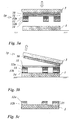
- a hot embossing film 2 is formed from a carrier film 20, a release layer 21, an electrically conductive transfer layer 22 and a primer layer 23, wherein the hot embossing film 2 is received on a heated die 3.
- the surface temperature of the embossing punch 3 may be, for example, 180 ° C to 190 ° C.
- the carrier film 20 may be, for example, a plastic film of 12 to 150 ⁇ m, preferably of 12 to 50 ⁇ m.
- the plastic film can for example consist of PET or BOPP.
- In the in Fig. 1 illustrated embodiment is a PET film of 19 to 23 microns thick.
- the release layer 21 can be made, for example, from a paint of the composition 20% vol. Polyacrylate, 70% vol. Methyl ethyl ketone and 10% vol. Butyl acetate be formed and form a layer of about 1 micron thick in the dried state.
- the electrically conductive transfer layer 22 consists of a binder portion and the conductive component. It may be in the transfer layer 22 to one of a paint, the composition of 56% -Vol. a powdery metallic component, such as gold, silver, aluminum, copper or an alloy of these metals, 19% -Vol. Binder and 25% vol. Solvent, act lacquer layer formed, which forms a transfer layer of about 25 microns thick when dried.
- binders for example, acrylate compounds and, for example, mixtures of ketones and aromatics can be used as solvent. However, it can also be a lacquer layer in which instead of the metallic component TiO 2 is provided, the composition being 25% by volume. TiO 2 , 10% vol. Binder and 65% vol. Solvent may be selected. Said binders form the first filler which is arranged between the electrically conductive regions of the transfer layer 22.
- the transfer layer 22 can be applied in a known manner by printing on the hot stamping foil.
- the primer layer 23 is also formed from a varnish, for example with the composition 26% vol. Binder, eg polyester or adhesive, 4% vol. SiO 2 , 50% vol. Methyl ethyl ketone and 20% vol. High boilers, such. B. cyclohexanone (boiling point 155 ° C).
- the application weight of the primer layer may be, for example, 0.5 to 0.8 g / m 2 .
- the SiO 2 particles in the primer layer serve as spacers during winding of the film and avoid "blocking" or an undesirable paint transfer to the back of the carrier film 20.
- the primer layer can also be an adhesive layer, preferably a layer of a hot melt adhesive , a UV-curable adhesive or a cold glue.
- the production of the hot embossing film can advantageously take place in a roll-to-roll process, wherein the abovementioned layers can all be transferred by printing processes.
- the rear side of the carrier film 20 faces the front side of the embossing stamp 3.
- the front side of the hot stamping foil 2, which is at the same time the front side primer layer 23, faces the upper side of the carrier substrate 1 and is brought into contact with it during the embossing process.
- the primer layer 23 acts as a primer layer or as an adhesive layer.
- the embossing stamp 3 is lifted off, the release layer 21 assisting the separation of the transfer layer 22 from the hot stamping film 2.
- Fig. 1c now shows the carrier substrate 1 with a post-treated transfer layer 22o, in which the binder is removed.
- the binder can be removed from the transferred to the substrate 1 transfer layer 22 in a sintering process.
- it may be intended to sinter for about 10 to 30 minutes while maintaining a temperature of about 500 ° C for about 10 minutes.
- organic components of the release layer, the transfer layer and the adhesive layer are expelled, wherein they enter the gas phase and generates a bond between the particles and the substrate in the non-volatile constituents of the transfer layer becomes.
- the particles of the non-expelled component are superficially connected to each other, so that consequently open pores form.
- the binder is only partially removed during the sintering process, and the remainder in a subsequent wet chemical process with subsequent cleaning and / or drying. It is also possible in this context that it is possible to dispense entirely with the layer 23, specifically if the binder in the transfer layer is sufficient to ensure a bond to the substrate during the embossing process. In this context, it is also possible that the layer 23 does not pass into the gas phase, and indeed when the residence time or the temperatures during the sintering process have not been chosen high enough.
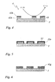
- the Fig. 2a to c Now show a second embodiment in which the transfer layer 22 of the hot stamping foil 2 is formed over the entire surface ( Fig. 2a ).
- the embossing stamp 3 has a surface structure which corresponds to the line structure to be transmitted, wherein the areas between the conductor tracks are recessed, so that the surface of the embossing stamp 3 is in contact only with the hot stamping foil 2 in the areas of the conductor tracks.
- the release layer is at least partially transferred and, for example, in a subsequent sintering process into the gas phase.
- the partially transferred primer layer may be designed to improve the adhesion of the areas of the transfer layer transferred to the carrier substrate 1, so that the areas of the transfer layer arranged under the recessed areas of the stamping die 3 can be easily removed.
- the primer has been removed in a sintering process.
- it may be intended to sinter for about 10 to 30 minutes while maintaining a temperature of about 500 ° C for about 10 minutes.
- organic components of the transfer layer, in particular the binder expelled and enter the gas phase.
- the Fig. 3a to c now show process steps for the construction of multilayer electrode layers.
- Fig. 3a shows a hot stamping foil 3p, which is pressed onto the carrier substrate 1 with the stamp 3.
- the hot embossing film 3p is made of a carrier film 30, a release layer 31, a first electrically conductive transfer layer 32a, a possible intermediate layer 33 (for example, to improve the adhesion during of printing), a second electrically conductive transfer layer 32b, and a primer layer 34.
- the two transfer layers 32a, 32b are transferred together, as in FIG Fig. 3b shown, wherein after the transfer, in turn, a sintering process is provided, which connects the two transfer layers both with each other and with the surface of the carrier substrate 1 permanently.
- the organic components of the release layer 31, the intermediate layer 33 and the primer layer 34 are expelled by the sintering process.
- the release layer 31 is set so that it does not remain on the hot stamping film 3p but on the electrode layer. The release layer 31 is therefore removed only in the sintering step.
- the Fig. 3c now shows the carrier substrate 1 with a patterned electrode layer 35, which consists of a lower sub-layer 32b and an upper sub-layer 32o.
- the carrier substrate 1 may be, for example, a doped silicon wafer, which is provided for the construction of a photovoltaic cell or a photovoltaic module.
- the lower sub-layer is 32b in the in Fig. 3c illustrated embodiment formed as a homogeneous, non-porous partially transparent electrode layer.
- the upper electrode layer 32o is designed as an open-pored electrode layer, the pores of which can be partially or completely filled with a filler in a further method step.
- the porosities are not only due to the proportion of the volatile component, but also due to the melting behavior the non-volatile component and the choice of the sintering temperature can be adjusted.
- the Fig. 4 now shows a very different possible use of porous structures on an example inert carrier.
- a porous matrix 45 formed of two transfer layers 42b and 42k having a similar structure as shown in FIG Fig. 3c shown.
- the upper porous transfer layer 42k acts as a catalyst for a chemical reaction.
- the transfer layer 42k has a very large surface area.
- the transfer layer 42k can be formed from a catalytically active material, but it can also be provided that the pores formed in the transfer layer 42k are coated on the surface with a catalytically active filler so as not to lose the enlarged surface.
- the chemical equilibrium is shifted from the starting components A and B to the end components C and D.
- Fig. 5 now shows a further embodiment in which starting from the in Fig. 2c illustrated intermediate step, the electrode layer 22o with a galvanically applied metallic layer 52 is covered.
- Fig. 6 shows a sixth embodiment in which, starting from the in Fig. 2c 1, an electrode layer 62 is formed on the carrier substrate 1, which is formed, for example, as an open-pore metallic layer of copper or silver, which has received good adhesion in itself as well as to the substrate by the sintering process and whose pores are filled with the filler PEDOT / PSS are filled.
- Such electrode formation can, for example, for the construction of photovoltaic Cells or modules may be provided on the basis of organic semiconductor layers.
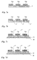
- Fig. 7a to 7e now show manufacturing stages for building a photovoltaic cell or module according to the principle of the dye cell.
- Fig. 7a shows as starting configuration analogous to that in Fig. 2c illustrated example on the carrier substrate 1, an open-cell electrode layer 72o, which is formed for example as a metallic layer of copper or silver with a thickness of about 60 microns.
- the carrier substrate 1 in this exemplary embodiment is an electrically conductive substrate, for example a metallic substrate made of gold vapor-deposited titanium foil with a total layer thickness of approximately 20 ⁇ m.
- the transfer layer 72o is then coated with titanate by, for example, coating a tetraalkylate solution.
- the titanate is converted in a subsequent temperature process at about 120 ° C and presence of high humidity in TiO x .
- the pores of the open-pored electrode layer are now coated with TiO x .
- the pores have an average diameter of 20 to 50 nm.
- the TiO x forms a layer with a layer thickness of about 3 nm on the pore surface.
- the transfer layer 72o is formed directly from a TiO 2 matrix, which forms the porous TiO 2 structure after the sintering process.
- the carrier substrate 1 is then cut into strips 1 ', each comprising a portion of the transfer layer 72o, as in FIG Fig. 7b shown.
- an electrically nonconductive carrier film 70 for example to a 19 ⁇ m thick PET film whose upper side is coated with an adhesive layer 71 ( Fig. 7c ).
- an adhesive layer for example, an acrylate compound with an application density of 2 g / m 2 can be provided.
- the coated electrode layer 72o is impregnated with a dye solution and transferred into an electrode layer 72g, as in FIG Fig. 7d shown.
- the dye solution can be, for example, a solution of ruthenium 2.2 AE-bipyridyl-4,4-AE-dicarboxylate 2 (NCS) 2.
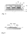
- Fig. 7e now shows a ready constructed electrochemical dye cell 7, in the first starting from the in Fig. 7g shown construction, in the mutually delimited regions of the electrode layer 72g each a redox electrolyte layer 73 is introduced, which may be, for example, a solution of iodine and potassium iodide.
- the redox electrolyte layer 73 may have a thickness of about 30 ⁇ m.
- a transparent electrode 74 is arranged above the redox electrolyte layer 73, which is covered by a transparent cover layer 75.
- Vertically arranged insulator layers 76 and 78 separate the photovoltaic cells arranged on the carrier film 70, the insulator layer covering one of the end sides of the superimposed electrode layer 72g, redox electrolyte layer 73 and transparent electrode 74. Between the two insulator layers 76 and 78, perpendicular connecting sections 77 are respectively provided for electrical connection of adjacent photovoltaic cells.
- the electrically conductive connection portion 77 is on that of the photovoltaic cell disposed on the opposite side of the insulator layer 76 and connects the electrode layer 72g of one adjacent photovoltaic cell with the transparent electrode 74 of the other adjacent photovoltaic cell.
- the insulator layer 78 covers the end faces of the carrier substrate 1 'facing away from the insulator layer 76, the electrode layer 72g and the transparent electrode 74.
- Fig. 8 11 shows an eighth exemplary embodiment, in which a transfer layer 822 formed from four partial transfer layers 822a to 822d is transferred onto the carrier substrate 1, for example onto a silicon wafer.
- the transferred partial transfer layers 822a to 822d are structured differently, so that, for example, a conductivity profile can be formed in the strip conductors or electrode regions.
- the partial transfer layers 822a to 822d are formed from different materials.
- the uppermost, outer partial transfer layer 822d may be made particularly weather-resistant
- the innermost partial transfer layer 822a may be designed to be particularly adherent
- the two intermediate transfer layers 822b and 822c arranged therebetween may have a high conductivity feature.
- the innermost sub-transfer layer 822a or the inner layer composite could, for example, contain aluminum, the outer sub-transfer layer 822d or the outer layer composite chrome.
- a sintering process may be provided, wherein it may further be provided to vary the sintering temperature and the sintering time for each layer application.
- FIG. 9 Now shows a ninth embodiment in plan view, which exemplifies the design options of the method according to the invention.
- the partial transfer layers 922a to 922c which give printed conductors 922, are successively transferred to the carrier substrate 1.
- the partial transfer layers 922a and 922b are in the in Fig. 5 illustrated embodiment in a plane, as are the areas of the partial transfer layer 922c, which do not cover areas of the partial transfer layers 922b.
- the partial transfer layers 922b may be, for example, electrode layers.
- the partial transfer layer 922c may be conductive lines electrically connecting the partial transfer layers 922b to each other.
- the partial transfer layers 922b and 922c may be formed of different materials so that the material properties may be optimally matched to the "electrode" and "line connection" functions.
- the partial transfer layer 922a may, for example, form a capacitor or an antenna arrangement in order to realize an additional function, such as a capacitor or an antenna for a built-in RFID chip.
- the material and / or the cross-sectional structure and / or the surface structure of the partial transfer layer 922a should be optimized for this function.
- a multiply structured surface structure may, for example, have a substantially larger surface area than a smooth surface structure and therefore have better electrical conductivity for high frequencies, ie be optimized with regard to the utilization of the so-called skin effect.
- Fig. 10 now shows a further embodiment in which on the carrier substrate 1 electrode layers 1022 are imprinted, which are personalized.
- the personalization has been carried out after transferring the electrode layer 1022 by embossing a surface profile, for example a hologram, in the surface of the electrode layer 1022.
- the personalization can be provided, for example, to apply a forgery-proof certificate of authenticity.
Landscapes
- Engineering & Computer Science (AREA)
- Manufacturing & Machinery (AREA)
- Microelectronics & Electronic Packaging (AREA)
- Photovoltaic Devices (AREA)
- Manufacturing Of Printed Wiring (AREA)
- Laminated Bodies (AREA)
- Catalysts (AREA)
- Exposure Of Semiconductors, Excluding Electron Or Ion Beam Exposure (AREA)
Applications Claiming Priority (1)
| Application Number | Priority Date | Filing Date | Title |
|---|---|---|---|
| DE102007027999A DE102007027999A1 (de) | 2007-06-14 | 2007-06-14 | Heißprägen von Strukturen |
Publications (2)
| Publication Number | Publication Date |
|---|---|
| EP2015620A2 true EP2015620A2 (fr) | 2009-01-14 |
| EP2015620A3 EP2015620A3 (fr) | 2010-10-06 |
Family
ID=39926495
Family Applications (1)
| Application Number | Title | Priority Date | Filing Date |
|---|---|---|---|
| EP08010671A Withdrawn EP2015620A3 (fr) | 2007-06-14 | 2008-06-12 | Imprégnation à chaud de structures |
Country Status (4)
| Country | Link |
|---|---|
| US (1) | US20080311330A1 (fr) |
| EP (1) | EP2015620A3 (fr) |
| JP (1) | JP2009010372A (fr) |
| DE (1) | DE102007027999A1 (fr) |
Cited By (2)
| Publication number | Priority date | Publication date | Assignee | Title |
|---|---|---|---|---|
| WO2015150330A1 (fr) * | 2014-03-31 | 2015-10-08 | Leibniz Universität Hannover | Procédé et dispositif d'assemblage de structures sur un substrat ainsi qu'agencement comprenant des structures assemblées de ce type |
| CN108687442A (zh) * | 2017-03-30 | 2018-10-23 | 法拉第未来公司 | 用于焊接的系统和方法 |
Families Citing this family (9)
| Publication number | Priority date | Publication date | Assignee | Title |
|---|---|---|---|---|
| DE102008014824B4 (de) * | 2008-03-18 | 2014-07-10 | Leonhard Kurz Stiftung & Co. Kg | Dotierfolien und deren Verwendung |
| WO2010126314A2 (fr) * | 2009-04-30 | 2010-11-04 | 한양대학교 산학협력단 | Cellule solaire au silicium comprenant une couche de nanotubes de carbone |
| WO2013187843A1 (fr) * | 2012-06-15 | 2013-12-19 | Agency For Science, Technology And Research | Procédé de gaufrage et dispositif de gaufrage |
| DE102012222416A1 (de) | 2012-12-06 | 2014-06-12 | Robert Bosch Gmbh | Verfahren zum Verbinden von wenigstens zwei Komponenten unter Verwendung eines Sinterprozesses |
| CN104009124B (zh) * | 2014-06-13 | 2018-09-18 | 苏州苏大维格光电科技股份有限公司 | 太阳能电池超精细电极转移薄膜、制备方法及其应用方法 |
| DE102015112909B3 (de) * | 2015-08-05 | 2017-02-09 | Leonhard Kurz Stiftung & Co. Kg | Verfahren und Vorrichtung zum Herstellen einer Mehrschichtfolie |
| GB201613051D0 (en) | 2016-07-28 | 2016-09-14 | Landa Labs (2012) Ltd | Applying an electrical conductor to a substrate |
| CN109809357A (zh) * | 2017-11-21 | 2019-05-28 | 锐迪科微电子(上海)有限公司 | 一种mems器件的晶圆级封装方法 |
| AU2023231024B2 (en) * | 2022-03-10 | 2025-08-14 | Commonwealth Scientific And Industrial Research Organisation | Transferrable electrode for printed electronics |
Citations (1)
| Publication number | Priority date | Publication date | Assignee | Title |
|---|---|---|---|---|
| DE68926361T2 (de) | 1988-03-25 | 1996-11-28 | Hitachi Techno Eng | Verfahren und Vorrichtung zur Aufbringung einer dünnen Schicht auf ein Substrat unter Druck |
Family Cites Families (24)
| Publication number | Priority date | Publication date | Assignee | Title |
|---|---|---|---|---|
| JPS5341978B2 (fr) * | 1973-05-02 | 1978-11-08 | ||
| JP2794960B2 (ja) * | 1991-02-19 | 1998-09-10 | 松下電器産業株式会社 | 焼結導体配線基板とその製造方法 |
| US5609704A (en) * | 1993-09-21 | 1997-03-11 | Matsushita Electric Industrial Co., Ltd. | Method for fabricating an electronic part by intaglio printing |
| JPH09510949A (ja) * | 1994-04-05 | 1997-11-04 | ザ・ユニバーシティ・オブ・クイーンズランド | 基体の被覆 |
| JPH10235986A (ja) * | 1997-02-21 | 1998-09-08 | Dainippon Printing Co Ltd | 静電印刷マスター版形成用の転写シートと静電印刷マスター版の製造方法および画像形成方法 |
| US5932643A (en) * | 1997-04-11 | 1999-08-03 | Ncr Corporation | Thermal transfer ribbon with conductive polymers |
| KR100536868B1 (ko) * | 1997-10-03 | 2006-02-28 | 다이니폰 인사츠 가부시키가이샤 | 전사시트 |
| TWI231293B (en) * | 1997-11-12 | 2005-04-21 | Jsr Corp | Transfer film |
| JPH11144628A (ja) * | 1997-11-12 | 1999-05-28 | Jsr Corp | 隔壁形成用転写フィルムおよびそれを用いたプラズマディスプレイパネルの製造方法 |
| US6743319B2 (en) * | 1998-09-30 | 2004-06-01 | Paralec Inc. | Adhesiveless transfer lamination method and materials for producing electronic circuits |
| US20030134095A1 (en) * | 2002-01-16 | 2003-07-17 | Bottari Frank J | Method of applying an edge electrode pattern to a touch screen |
| US6280552B1 (en) * | 1999-07-30 | 2001-08-28 | Microtouch Systems, Inc. | Method of applying and edge electrode pattern to a touch screen and a decal for a touch screen |
| DE19940015B9 (de) * | 1999-08-24 | 2004-09-09 | Deutsches Zentrum für Luft- und Raumfahrt e.V. | Verfahren und Vorrichtung zur Herstellung einer Elektrode |
| JP2001085822A (ja) * | 1999-09-16 | 2001-03-30 | Dainippon Printing Co Ltd | 転写版の作製方法と転写版、および配線基板の製造方法と配線基板 |
| US6402866B1 (en) * | 1999-09-30 | 2002-06-11 | International Business Machines Corporation | Powdered metallic sheet method for deposition of substrate conductors |
| JP2002243692A (ja) * | 2001-02-19 | 2002-08-28 | Riken Corp | 窒素酸化物ガスセンサ |
| JP2003031948A (ja) * | 2001-07-12 | 2003-01-31 | Matsushita Electric Ind Co Ltd | セラミック多層基板の製造方法 |
| JP2003229252A (ja) * | 2002-02-01 | 2003-08-15 | Sharp Corp | 転写フィルムを用いた有機led素子の製造方法 |
| DE10210696A1 (de) * | 2002-03-12 | 2003-10-02 | Elringklinger Ag | Verfahren zum Herstellen einer Deckschicht auf einem Substrat für eine Kathoden-Elektrolyt-Anoden-Einheit |
| JP4357937B2 (ja) * | 2003-11-18 | 2009-11-04 | 大日本印刷株式会社 | レーザー転写フィルム及びカラーフィルターの製造方法 |
| US7494607B2 (en) * | 2005-04-14 | 2009-02-24 | E.I. Du Pont De Nemours And Company | Electroconductive thick film composition(s), electrode(s), and semiconductor device(s) formed therefrom |
| US20080083484A1 (en) * | 2006-09-28 | 2008-04-10 | Graciela Beatriz Blanchet | Method to form a pattern of functional material on a substrate |
| EP2153708A1 (fr) * | 2007-05-24 | 2010-02-17 | Basf Se | Procédé de réalisation de laminés de base dotés d'un revêtement métallique |
| DE102007027998A1 (de) * | 2007-06-14 | 2008-12-18 | Leonhard Kurz Gmbh & Co. Kg | Heißprägen von Leiterbahnen auf Photovoltaik-Silizium-Wafer |
-
2007
- 2007-06-14 DE DE102007027999A patent/DE102007027999A1/de not_active Ceased
-
2008
- 2008-06-10 US US12/136,540 patent/US20080311330A1/en not_active Abandoned
- 2008-06-12 EP EP08010671A patent/EP2015620A3/fr not_active Withdrawn
- 2008-06-16 JP JP2008157179A patent/JP2009010372A/ja active Pending
Patent Citations (1)
| Publication number | Priority date | Publication date | Assignee | Title |
|---|---|---|---|---|
| DE68926361T2 (de) | 1988-03-25 | 1996-11-28 | Hitachi Techno Eng | Verfahren und Vorrichtung zur Aufbringung einer dünnen Schicht auf ein Substrat unter Druck |
Cited By (2)
| Publication number | Priority date | Publication date | Assignee | Title |
|---|---|---|---|---|
| WO2015150330A1 (fr) * | 2014-03-31 | 2015-10-08 | Leibniz Universität Hannover | Procédé et dispositif d'assemblage de structures sur un substrat ainsi qu'agencement comprenant des structures assemblées de ce type |
| CN108687442A (zh) * | 2017-03-30 | 2018-10-23 | 法拉第未来公司 | 用于焊接的系统和方法 |
Also Published As
| Publication number | Publication date |
|---|---|
| US20080311330A1 (en) | 2008-12-18 |
| EP2015620A3 (fr) | 2010-10-06 |
| DE102007027999A1 (de) | 2008-12-18 |
| JP2009010372A (ja) | 2009-01-15 |
Similar Documents
| Publication | Publication Date | Title |
|---|---|---|
| DE102007027999A1 (de) | Heißprägen von Strukturen | |
| DE69320971T2 (de) | Vakuum-beschichtung und härtung von flüssigen monomeren | |
| DE69901103T2 (de) | Durch abscheidung von schichten gebildete gasverteilerstruktur für brennstoffzellen | |
| EP1676330B1 (fr) | Méthode pour structurer des couches fonctionelles electriques au moyen d'un film de transfer et méthode pour structurer l'adhesif | |
| EP2003698A2 (fr) | Estampage à chaud des pistes conductrices sur des plaquettes de silicium photovoltaïques | |
| EP2561730B1 (fr) | Procédé de transfert permettant la fabrication de structures conductrices au moyen de nano-encres | |
| KR102375841B1 (ko) | 가요성 기판상에 전자 장치를 형성하는 방법 | |
| EP3198660B1 (fr) | Procédé pour appliquer une couche protectrice pour la fabrication d'un semi-produit | |
| JP2025519017A (ja) | グラフェン系粒子と結合した液体金属液滴からなる懸濁液、コロイドまたは網状組織、それぞれのインク、透明伸縮性導体およびそれらの獲得プロセス | |
| WO2009156060A1 (fr) | Système de modulateur de lumière, à transparence commutable, et son procédé de fabrication | |
| EP2502471B1 (fr) | Fabrication de structures de conducteur sur des films en matière plastique au moyen de nano-encres | |
| DE102007051930A1 (de) | Verfahren zur Herstellung einer Leiterbahnstruktur | |
| DE102010040826B4 (de) | Verfahren zur Immobilisierung von Nanopartikeln auf thermoplastischen Kunststoffoberflächen sowie immobilisierte Nanopartikel | |
| EP2157641B1 (fr) | Procédé de fabrication d'une plaque bipolaire et plaque bipolaire pour une batterie bipolaire au plomb | |
| US8388790B2 (en) | Multilayered body comprising an electroconductive polymer layer and method for the production thereof | |
| EP2157642A2 (fr) | Procédé de fabrication d'une cellule bipolaire et cellule bipolaire pour une batterie bipolaire | |
| EP4010913B1 (fr) | Procédé de fabrication d'un élément fonctionnel magnétique imprimé, et élément fonctionnel magnétique imprimé | |
| DE102008051656A1 (de) | Verfahren zum Aufbringen einer metallischen Elektrode auf eine Polymerschicht | |
| DE102012106607B4 (de) | Verfahren zur Versiegelung von Modulen mit optoelektronischen Bauelementen | |
| DE102006033887B4 (de) | Verfahren zur Herstellung eines Mehrschichtkörpers mit leitfähiger Polymerschicht | |
| DE102012210615A1 (de) | Leitpaste und Verfahren zur Herstellung einer Solarzelle | |
| DE102008036320B4 (de) | Verfahren zur Herstellung einer Bipolarplatte und Bipolarplatte für eine bipolare Batterie | |
| DE102008014824B4 (de) | Dotierfolien und deren Verwendung | |
| DE102014213978A1 (de) | Verfahren zur Herstellung eines organischen Halbleiterbauteils und organisches Halbleiterbauteil | |
| EP2030697A2 (fr) | Procédé de fabrication d'un revêtement sur un support et outil de pression ou contre-outil |
Legal Events
| Date | Code | Title | Description |
|---|---|---|---|
| PUAI | Public reference made under article 153(3) epc to a published international application that has entered the european phase |
Free format text: ORIGINAL CODE: 0009012 |
|
| PUAI | Public reference made under article 153(3) epc to a published international application that has entered the european phase |
Free format text: ORIGINAL CODE: 0009012 |
|
| AK | Designated contracting states |
Kind code of ref document: A2 Designated state(s): AT BE BG CH CY CZ DE DK EE ES FI FR GB GR HR HU IE IS IT LI LT LU LV MC MT NL NO PL PT RO SE SI SK TR |
|
| AX | Request for extension of the european patent |
Extension state: AL BA MK RS |
|
| PUAL | Search report despatched |
Free format text: ORIGINAL CODE: 0009013 |
|
| AK | Designated contracting states |
Kind code of ref document: A3 Designated state(s): AT BE BG CH CY CZ DE DK EE ES FI FR GB GR HR HU IE IS IT LI LT LU LV MC MT NL NO PL PT RO SE SI SK TR |
|
| AX | Request for extension of the european patent |
Extension state: AL BA MK RS |
|
| 17P | Request for examination filed |
Effective date: 20110404 |
|
| AKX | Designation fees paid |
Designated state(s): AT BE BG CH CY CZ DE DK EE ES FI FR GB GR HR HU IE IS IT LI LT LU LV MC MT NL NO PL PT RO SE SI SK TR |
|
| GRAP | Despatch of communication of intention to grant a patent |
Free format text: ORIGINAL CODE: EPIDOSNIGR1 |
|
| STAA | Information on the status of an ep patent application or granted ep patent |
Free format text: STATUS: THE APPLICATION IS DEEMED TO BE WITHDRAWN |
|
| 18D | Application deemed to be withdrawn |
Effective date: 20130219 |