EP2020673A2 - Aberrationskorrektursystem - Google Patents
Aberrationskorrektursystem Download PDFInfo
- Publication number
- EP2020673A2 EP2020673A2 EP08252352A EP08252352A EP2020673A2 EP 2020673 A2 EP2020673 A2 EP 2020673A2 EP 08252352 A EP08252352 A EP 08252352A EP 08252352 A EP08252352 A EP 08252352A EP 2020673 A2 EP2020673 A2 EP 2020673A2
- Authority
- EP
- European Patent Office
- Prior art keywords
- magnetic
- multipole
- electric field
- optical axis
- stages
- Prior art date
- Legal status (The legal status is an assumption and is not a legal conclusion. Google has not performed a legal analysis and makes no representation as to the accuracy of the status listed.)
- Granted
Links
Images



Classifications
-
- H—ELECTRICITY
- H01—ELECTRIC ELEMENTS
- H01J—ELECTRIC DISCHARGE TUBES OR DISCHARGE LAMPS
- H01J37/00—Discharge tubes with provision for introducing objects or material to be exposed to the discharge, e.g. for the purpose of examination or processing thereof
- H01J37/02—Details
- H01J37/04—Arrangements of electrodes and associated parts for generating or controlling the discharge, e.g. electron-optical arrangement or ion-optical arrangement
- H01J37/153—Electron-optical or ion-optical arrangements for the correction of image defects, e.g. stigmators
-
- H—ELECTRICITY
- H01—ELECTRIC ELEMENTS
- H01J—ELECTRIC DISCHARGE TUBES OR DISCHARGE LAMPS
- H01J37/00—Discharge tubes with provision for introducing objects or material to be exposed to the discharge, e.g. for the purpose of examination or processing thereof
- H01J37/26—Electron or ion microscopes; Electron or ion diffraction tubes
-
- H—ELECTRICITY
- H01—ELECTRIC ELEMENTS
- H01J—ELECTRIC DISCHARGE TUBES OR DISCHARGE LAMPS
- H01J2237/00—Discharge tubes exposing object to beam, e.g. for analysis treatment, etching, imaging
- H01J2237/153—Correcting image defects, e.g. stigmators
- H01J2237/1534—Aberrations
-
- H—ELECTRICITY
- H01—ELECTRIC ELEMENTS
- H01J—ELECTRIC DISCHARGE TUBES OR DISCHARGE LAMPS
- H01J2237/00—Discharge tubes exposing object to beam, e.g. for analysis treatment, etching, imaging
- H01J2237/26—Electron or ion microscopes
- H01J2237/262—Non-scanning techniques
-
- H—ELECTRICITY
- H01—ELECTRIC ELEMENTS
- H01J—ELECTRIC DISCHARGE TUBES OR DISCHARGE LAMPS
- H01J2237/00—Discharge tubes exposing object to beam, e.g. for analysis treatment, etching, imaging
- H01J2237/26—Electron or ion microscopes
- H01J2237/28—Scanning microscopes
- H01J2237/2802—Transmission microscopes
Definitions
- the present invention relates to an aberration correction system for use in a transmission electron microscope and, more particularly, to an aberration correction system using three stages of multipole elements each producing a field of 3-fold symmetry.
- spherical aberration that is one of such aberrations limits the spatial resolution because an axisymmetric lens always has a positive spherical aberration coefficient. This creates an intrinsic problem.
- This aberration correction system has a first transfer lens, a first hexapole element, a second transfer lens, and a second hexapole element arranged in turn.
- each transfer lens has two axisymmetric lenses.
- An aberration correction system having two stages of multipole elements each having a thickness along the optical axis is shown in patent reference 1.
- This system has two stages of multipole elements (e.g., hexapole elements) and a transfer lens interposed between them.
- Each multipole element produces a field of 3-fold symmetry, generating a 3-fold astigmatism and a negative spherical aberration.
- the rear stage of multipole element operates to cancel out the 3-fold astigmatism produced by the front stage of multipole element and, therefore, the whole optical system produces a negative spherical aberration. Consequently, where an axisymmetric lens (e.g.,an objectivelens)producing a positivesphericalaberration is disposed ahead of or behind the system, the spherical aberration in the whole optical system is reduced.
- an axisymmetric lens e.g.,an objectivelens
- the above-described aberration-correcting techniques correct aberrations only up to the fourth order and cannot achieve complete correction of higher-order aberrations.
- fifth-order spherical aberration can be corrected by optically controlling the distance between the objective lens and the aberration corrector but astigmatism of the same order (i.e., 6-fold astigmatism) cannot be corrected. Because this is a factor limiting aberration correction, it cannot be expected that the spatial resolution will be improved further.
- An actual multipole element has a finite thickness along theopticalaxis. Where this multipole element produces a magnetic or electric field with 3-fold symmetry, if the spherical aberration is corrected by the multipole element, higher-order aberrations dependent on the thickness are induced. Furthermore, the combination of the two stages produces higher-order aberrations. Consequently, the range of incident angles of the electron beam that can be aberration-corrected is limited. This limitation makes it difficult to reduce diffraction aberration.
- This limitation to the angles is further described by referring to the Ronchigram of Fig. 7 .
- This diagram is obtained when an electron beam passing through two stages of multipole elements is corrected for aberrations, each of the multipole elements producing a magnetic field of 3-fold symmetry with respect to the optical axis.
- a low-contrast region appearing in the center of the diagram corresponds to the angle of incidence of the electron beam on each multipole element, the beam having been appropriately corrected for aberrations.
- a maximum value of the angle of incidence is roughly described, a maximum circle centered at the central point of the region and including only the region is fitted.
- the angle of incidence of the electron beam is computed from the radius of the circle. It can be seen from the diagram of Fig. 7 that the maximum incident angle of the electron beam that has been appropriately corrected for aberrations is about 50 mrad.
- the angle of incidence of the electron beam that can be corrected for aberrations is 50 mrad at maximum. It is difficult to appropriately correct the electron beam having a greater angle of incidence for aberrations. Accordingly, if one tries to reduce diffraction aberration, the spatial resolution is limited due to the limitation on the angle of incidence.
- an aberration correction system which is for use in an electron microscope and which corrects the above-described higher-order aberrations while holding a negative spherical aberration.
- an aberration correction system having three stages of multipole elements arranged in a row along an optical axis, each of the multipole elements having a thickness along the optical axis.
- the three stages of multipole elements include a front stage of multipole element, a middle stage of multipole element, and a rear stage of multipole element.
- the front stage of multipole element produces a first magnetic or electric field that shows a 3-fold symmetry with respect to the optical axis.
- the middle stage of multipole element produces a second magnetic or electric field that shows a 3-fold symmetry with respect to the optical axis.
- the rear stage of multipole element produces a third magnetic or electric field that shows a 3-fold symmetry with respect to the optical axis.
- a distribution of a magnetic or electric field of 3-fold symmetry is produced in a direction not to cancel out an astigmatism of 3-fold symmetry produced from the first magnetic or electric field or from the third magnetic or electric field.
- a distribution of a magnetic or electric field of 3-fold symmetry is produced in a direction not to cancel out an astigmatism of 3-fold symmetry produced from the first magnetic or electric field or from the third magnetic or electric field.
- An aberration of 3-fold symmetry produced by the front stage of multipole element is rotated using the middle stage of multipole element.
- An aberration of 3-fold symmetry produced by the middle stage of multipole element is rotated using the rear stage of multipole element.
- the fields produced by the three stages of multipole elements are combined to cancel out their mutual astigmatisms of 3-fold symmetry.
- the aforementioned rotation is an electron optical angular rotation made when a field produced by one multipole element is transferred to the next multipole element.
- Rotating action of each lens is taken into consideration. That is, a magnetic lens produces a rotating action about the optical axis, as well as a transferring action and a magnification-varying action.
- the rotating action is affected by the accelerating voltage and by the strength of the magnetic field.
- the rotational positional relationship between the 3-fold astigmatisms of two multipole elements must be discussed taking account of rotation induced by the lens.
- rotational positional relationships are set forth on the assumption that an angle given by this rotation is zero. That the electron optical rotational relation is taken into consideration means that this rotation is taken into consideration.
- the angular relational relationship between the magnetic or electric fields produced by the multipole elements is set as follows. Any one of the second and third magnetic or electric field is rotated through an angle of 40° relative to the first magnetic or electric field, taking account of the rotating action of an electron optical lens within a plane perpendicular to the optical axis. The other is rotated through 80° relative to the first magnetic or electric field, taking account of the rotating action of the electron optical lens within the plane perpendicular to the optical axis. The second magnetic or electric field and the third magnetic or electric field are so distributed that they are rotated in the same direction. Afield of 3-fold symmetry has a rotational symmetry of 120°. Where a mirror-symmetric system is taken into consideration, rotational positional relationships given by 40° and 80° are equivalent to 120° ⁇ m ⁇ 40° and 120° ⁇ m ⁇ 80°, respectively.
- the angular relational relationship between the magnetic or electric fields produced by the multipole elements is set as follows.
- the second magnetic or electric field is so distributed that it is rotated through 120° ⁇ m ⁇ about 72° (where m is an integer) relative to the first magnetic or electric field, taking account of the rotating action of an electron optical lens within a plane perpendicular to the optical axis.
- the third magnetic or electric field is so distributed that it is rotated through 120° ⁇ m ⁇ about 24° relative to the first magnetic or electric field, taking account of the rotating action of the electron optical lens within the plane perpendicular to the optical axis.
- 3-fold astigmatism and 6-fold astigmatism may be removed while producing a negative spherical aberration and, therefore, the spatial resolution is improved. Furthermore, the range of incident angles in which aberration correction can be made can be widened. This reduces diffraction aberration and further improves the spatial resolution.
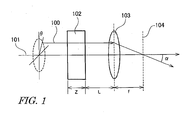
- Fig. 1 is a schematic ray diagram of aberrations produced on a surface of a specimen when the electron beam has passed through the single stage of multipole element.
- the single stage of multipole element 102 (e.g., a hexapole element) and the objective lens 103 are arranged in a row along the optical axis 101. It is assumed that the multipole element 102 produces a magnetic or electric field that shows 3-fold symmetry with respect to the optical axis 101. After passing through the multipole element 102, the beam 100 is focused onto the surface 104 of the specimen by the objective lens 103.
- the complex angle ⁇ 0 is represented by two variables ⁇ and ⁇ .
- the variable ⁇ is the angle at which the beam impinges on the specimen.
- the variable ⁇ is a phase angle (azimuth).
- z be the thickness (length) of the multipole element 102 along the optical axis 101.
- f be the focal distance of the objective lens. It is assumed that the optical distance L between the multipole element 102 and the objective lens 103 is 0. The optical distance L can be adjusted, for example, by inserting a transfer lens between the multipole element 102 and the objective lens 103.
- r be the position of the electron beam 100 on the specimen surface 104.
- r ' be the tilt (angle to the optical axis) of the beam.
- 2 3360 ⁇ f 5 ⁇ ⁇ ⁇ 0 5 ⁇ z 8 r ⁇ - 1 f ⁇ A 3 ⁇ ⁇ ⁇ 0 2 ⁇ z + A 3 2 3 ⁇ f 3 ⁇ ⁇ ⁇ 0 ⁇ ⁇ ⁇
- Each term of the right sides of Eqs. (3) and (4) represents an aberration.
- the first term of the right side of each equation indicates the second-order, 3-fold astigmatism.
- the second term indicates the third-order negative spherical aberration.
- the third and fourth terms indicate the fourth-order, three-lobe aberrations.
- the first term of Eq. (7) is a negative spherical aberration intentionally produced to cancel out the spherical aberration in the objective lens.
- the second term produces a higher-order aberration (6-fold astigmatism) because the two stages of multipole elements are prepared and that the 3-fold astigmatism produced from the first stage of multipole element is canceled out.
- three stages of multipole elements are prepared.
- the multipole elements are so operated that a combination of any two stages does not cancel out a 3-fold astigmatism. Rather, the three stages of multipole elements cancel out 3-fold astigmatisms. In this way, an optical system that cancels out the higher-order aberration is built.
- FIG. 2a is a schematic diagram of an aberration correction system associated with an embodiment of the present invention.
- the aberration correction system associated with the present embodiment is equipped with three stages of multipole elements producing fields of 3-fold symmetry with respect to the optical axis 11.
- an electron beam 10 passes from a front stage of multipole element 21 to a rear stage of multipole element 23. Then, the beam 10 passes through the coma-free plane 41 of an objective lens 40 that substantially corresponds the front focal plane of the objective lens 40. Subsequently, the beam is focused onto a specimen surface 42.
- each multipole element is a hexapole element. Another example is a dodecapole (12-pole) element.
- Each multipole element may have any number of poles as long as the element produces a field of 3-fold symmetry with respect to the optical axis 11.
- the field of 3-fold symmetry (second field of 3-fold symmetry) produced by the middle stage of multipole element 22 is so distributed that it has been rotated through 40° relative to the field of 3-fold symmetry (first field of 3-fold symmetry) produced by the front stage of multipole element 21 within the plane perpendicular to the optical axis 11.
- the field of 3-fold symmetry (third field of 3-fold symmetry) produced by the rear stage of multipole element 23 is so distributed that it has been rotated through 80° relative to the field of 3-fold symmetry produced by the front stage of multipole element 21 within the plane perpendicular to the optical axis 11.
- the fields of 3-fold symmetry produced by the middle stage of multipole element 22 and the rear stage of multipole element 23, respectively, are so distributed that they have been rotated in the same direction relative to the field of 3-fold symmetry produced by the front stage of multipole element 21.
- a 3 ⁇ A a 3 exp i ( 3 ⁇ )
- a negative spherical aberration coefficient does not depend on the rotational positional relationships among the fields of 3-fold symmetry. Therefore, the negative spherical aberration coefficient has a magnitude that is three times as high as the intensity of the coefficient produced by one field of 3-fold symmetry. Consequently, the negative spherical aberration coefficient can be used for correction of the spherical aberration in the objective lens.
- the middle stage of multipole element 22 may produce a field of 3-fold symmetry rotated through 80° relative to the field of 3-fold symmetry produced by the front stage of multipole element 21, and the rear stage of multipole element 23 may produce a field of 3-fold symmetry rotated through 40° relative to the field of 3-fold symmetry produced by the front stage of multipole element 21.
- the 3-fold astigmatism and 6-fold astigmatism are canceled out while a negative spherical aberration is produced.
- the multipole elements producing the above-described three fields of 3-fold symmetry are arranged as follows. Any one of the middle stage of multipole element 22 and the rear stage of multipole element 23 is rotated through 40° relative to the front stage of multipole element 21 within the plane perpendicular to the optical axis 11. The other is rotated through 80° within the plane perpendicular to the optical axis 11. At this time, the middle stage of multipole element 22 and the rear stage of multipole element 23 are disposed to be rotated in the same direction.
- Figs. 2b-2d show one example of arrangement of the multipole elements based on the above-described arrangement.
- the arrangement of the front stage of multipole element 21 as viewed along the direction indicated by the arrow A from the origin O on the optical axis 11 shown in Fig. 2a is indicated by 21a.
- the arrangement of the middle stage of multipole element 22 is indicated by 22a.
- the arrangement of the rear stage of multipole element 23 is indicated by 23a.
- This rotational positional relationship needs to be noticed after a rotation is made by the transfer lens. If an electron optical rotation of 40° is achieved by the transfer lens, it does not matter whether the rotation of 40° is made physically.
- a field of 3-fold symmetry has a rotational symmetry of 120°. Where a mirror-symmetric system is considered, the rotational positional relationships given by 40° and 80°, respectively, are equivalent to 120° ⁇ m ⁇ 40° and 120° ⁇ m ⁇ 80°, respectively.
- a 3A , A 3B , and A 3C be 3-fold astigmatism coefficients produced by the front, middle, and rear stages of multipole elements, respectively.
- the tilt of the electron beam leaving the third stage of multipole element with respect to the 6-fold astigmatism is given by
- Fig. 8 is a graph in which the amount of a higher-order aberration (6-fold astigmatism) produced when two stages of multipole elements are used is plotted on the vertical axis and the angle made between the multipole elements producing the 3-fold astigmatism coefficients A 3A and A 3C is plotted on the horizontal axis.
- the amount of the higher-order aberration has been normalized to 1 using Eq. (11) to indicate the relative amount of the 6-fold astigmatism.
- the system is so set that the 3-fold astigmatisms are canceled out by combining the fields of 3-fold symmetry produced by the three stages of multipole elements.
- the field of 3-fold symmetry (second field of 3-fold symmetry) produced by the front stage of multipole element 22 is distributed to have been rotated through about 72° relative to the field of 3-fold symmetry (first field of 3-fold symmetry) produced by the front stage of multipole element 21 within the plane perpendicular to the optical axis 11.
- the field of 3-fold symmetry (third field of 3-fold symmetry) produced by the rear stage of multipole element 23 is distributed to have been rotated through about 24° relative to the field of 3-fold symmetry produced by the front stage of multipole element 21 within the plane perpendicular to the optical axis 11.
- a 3-fold field returns to its original state if rotated through 120°. Furthermore, a 3-fold field can be realized by a mirror-symmetric optical system.
- the rotational positional relationship described so far can be generalized as follows from geometrical symmetry.
- the angle made between the first stage of multipole element and the second stage of multipole element can be generalized to 120° ⁇ m ⁇ about 72° (where m is an integer) within the plane perpendicular to the optical axis 11.
- the angle made between the second stage of multipole element and the third stage of multipole element can be generalized to 120° ⁇ m ⁇ 24° within the plane perpendicular to the optical axis 11.
- a negative spherical aberration coefficient does not depend on the rotational positional relationship between the fields of 3-fold symmetry and thus the combination of the intensities created by the three fields of 3-fold symmetry can be used for correction of the spherical aberration in an objective lens.
- Figs. 2e-2f show one example of the arrangement of the multipole elements based on the above-described arrangements.
- the arrangement of the front stage of multipole element 21 as viewed along the direction indicated by the arrow A from the origin O on the optical axis 11 shown in Fig. 2a is indicated by 21b.
- the arrangement of the middle stage of multipole element 22 is indicated by 22b.
- the arrangement of the rear stage of multipole element 23 is indicated by 23b.
- the three stages of multipole elements 21, 22, and 23 producing the fields of 3-fold symmetry as described above cancel out the 3-fold astigmatisms while producing a negative spherical aberration. Furthermore, 6-fold astigmatism that is a higher-order aberration is also corrected.
- rotating means for rotating the multipole elements 21, 22, and 23 within the plane perpendicular to the optical axis 11 may be mounted.
- a pair of first transfer lenses 31 may be mounted between the front stage of multipole element 21 and the middle stage of multipole element 22, and a pair of second transfer lenses 32 may be mounted between the middle stage of multipole element 22 and the rear stage of multipole element 23.
- the first transfer lenses 31 of the pair have two axisymmetric lenses 31a and 31b and transfer an image equivalent to the image obtained by the front stage of multipole element 21 to the middle stage of multipole element 22.
- the second transfer lenses 32 of the pair have two axisymmetric lenses 32a and 32b and transfer an image equivalent to the image obtained by the middle stage of multipole element 22 to the rear stage of multipole element 23. That is, the optical distance between the multipole elements is reduced down to 0 by the pairs of transfer lenses 31 and 32.
- the pairs of transfer lenses 31 and 32 only act to transfer the equivalent images to between the multipole elements and so do not affect the optical characteristics relying on the three fields of 3-fold symmetry.
- a distance can be secured between the multipole elements. This provides wider latitude in disposing the multipole elements.
- a pair of third transfer lenses 33 may be mounted between the objective lens 40 and the rear stage of multipole element 23, in addition to the first and second transfer lenses 31, 32.
- the third transfer lenses of the pair have two axisymmetric lenses 33a and 33b and transfer an image equivalent to the image obtained by the rear stage of multipole element 23 to the objective lens 40. That is, the optical distance between them is zero.
- the third transfer lenses of the pair only act to transfer the equivalent image to the objective lens 40 in the same way as the first and second transfer lenses 31, 32. Therefore, the third lenses do not affect the optical characteristics relying on the three fields of 3-fold symmetry. This offers wider latitude in disposing the rear stage of multipole element 23 and the objective lens 40.
- Fig. 5 shows an example of transmission electron microscope 50 using the aberration correction system as an illumination system aberration corrector.
- An electron gun 51 produces an electron beam (not shown) under control of a high-voltage control portion 58 and accelerates the beam to a desired energy.
- a first condenser lens 52 then focuses the accelerated beam.
- the focused beam passes through an illumination system aberration corrector 53. At this time, the aforementioned aberration correction is performed.
- the beam leaving the aberration corrector 53 is focused by a second condenser lens 54 and passes through an objective lens and a specimen stage 55. A specimen is placed on the stage 55.
- the electron beam transmitted through the specimen is enlarged by an intermediate projector lens 56. Then, the beam impinges on a fluorescent screen (not shown) in an observation chamber 57. The image of the specimen projected onto the fluorescent screen is captured by a camera.
- the objective lens When the beam passes through the objective lens and specimen stage 55, the objective lens further focuses the beam.
- a positive spherical aberration due to the objective lens acts to increase the spot diameter of the beam on the specimen surface.
- the positive spherical aberration is canceled out by a negative spherical aberration produced by the illumination system aberration corrector 53. Consequently, a very small spot of the beam is obtained on the specimen surface.
- Fig. 6 shows an example of a transmission electron microscope, indicated by 60, using an aberration correction system associated with one embodiment of the present invention as an imaging system aberration corrector.
- the microscope 60 has an electron gun 61 that produces an electron beam (not shown) under control of a high voltage control portion 68 and accelerates the beam to a desired energy.
- the accelerated beam is then focused by a first condenser lens 62 and a second condenser lens 63.
- the focused beam is then passed through an objective lens and a specimen stage 64. Then, the beam is made to hit a specimen on the specimen stage.
- the electron beam transmitted through the specimen passes through an imaging system aberration corrector 65. At this time, the aforementioned aberration correction is performed.
- the beam passed through the aberration corrector 65 is enlarged by an intermediate projector lens 66 and impinges on a fluorescent screen (not shown) in an observation chamber 67.
- the specimen image projected onto the fluorescent screen is captured by a camera.
- the imaging system aberration corrector 65 When the electron beam passes through the imaging system aberration corrector 65, a positive spherical aberration produced by the objective lens is canceled out by a negative spherical aberration possessed by the aberration corrector 65.
- This aberration corrector removes 3-fold astigmatisms, 6-fold astigmatism, and other astigmatisms. Consequently, the spatial resolution of the transmission electron microscope is improved.
- Aberration correctionmade by the imaging system aberration corrector 65 widens the range of incident angles of the electron beam in which aberration correction can be made. This in turn reduces diffraction aberration induced by an aperture (not shown). In consequence, the spatial resolution of the transmission electron microscope is improved further.
- any one of the illumination system aberration corrector 53 and imaging system aberration corrector 65 is installed in a transmission electron microscope.
- a transmission electron microscope may also be equipped with both of these aberration correctors.
Landscapes
- Chemical & Material Sciences (AREA)
- Analytical Chemistry (AREA)
- Electron Beam Exposure (AREA)
- Analysing Materials By The Use Of Radiation (AREA)
Applications Claiming Priority (2)
| Application Number | Priority Date | Filing Date | Title |
|---|---|---|---|
| JP2007202134 | 2007-08-02 | ||
| JP2008107375A JP5226367B2 (ja) | 2007-08-02 | 2008-04-17 | 収差補正装置 |
Publications (3)
| Publication Number | Publication Date |
|---|---|
| EP2020673A2 true EP2020673A2 (de) | 2009-02-04 |
| EP2020673A3 EP2020673A3 (de) | 2010-08-11 |
| EP2020673B1 EP2020673B1 (de) | 2014-01-15 |
Family
ID=39929645
Family Applications (1)
| Application Number | Title | Priority Date | Filing Date |
|---|---|---|---|
| EP08252352.3A Active EP2020673B1 (de) | 2007-08-02 | 2008-07-10 | Aberrationskorrektursystem |
Country Status (3)
| Country | Link |
|---|---|
| US (1) | US7723683B2 (de) |
| EP (1) | EP2020673B1 (de) |
| JP (1) | JP5226367B2 (de) |
Cited By (1)
| Publication number | Priority date | Publication date | Assignee | Title |
|---|---|---|---|---|
| EP3419043A1 (de) * | 2017-06-20 | 2018-12-26 | Jeol Ltd. | Verzerrungskorrekturverfahren und elektronenmikroskop |
Families Citing this family (15)
| Publication number | Priority date | Publication date | Assignee | Title |
|---|---|---|---|---|
| JP5623719B2 (ja) * | 2008-10-06 | 2014-11-12 | 日本電子株式会社 | 荷電粒子線装置の色収差補正装置及びその補正方法 |
| EP2325862A1 (de) * | 2009-11-18 | 2011-05-25 | Fei Company | Korrektor für axiale Aberrationen einer teilchenoptischen Linse |
| JP5502595B2 (ja) | 2010-05-18 | 2014-05-28 | 日本電子株式会社 | 球面収差補正装置および球面収差補正方法 |
| WO2012014870A1 (ja) * | 2010-07-27 | 2012-02-02 | 株式会社日立ハイテクノロジーズ | 収差補正装置およびそれを用いた荷電粒子線装置 |
| JP5545869B2 (ja) | 2010-11-16 | 2014-07-09 | 日本電子株式会社 | 荷電粒子線の軸合わせ方法及び荷電粒子線装置 |
| JP5677081B2 (ja) * | 2010-12-28 | 2015-02-25 | 株式会社日立ハイテクノロジーズ | 荷電粒子線装置 |
| JP5934517B2 (ja) * | 2012-02-24 | 2016-06-15 | 日本電子株式会社 | 色収差補正装置及び色収差補正装置の制御方法 |
| US8541755B1 (en) | 2012-05-09 | 2013-09-24 | Jeol Ltd. | Electron microscope |
| US10096448B2 (en) | 2015-04-27 | 2018-10-09 | National University Corporation Nagoya University | Spherical aberration corrector for electromagnetic lens for charged particle beam |
| JP6943779B2 (ja) | 2018-01-24 | 2021-10-06 | 日本電子株式会社 | 収差補正装置および電子顕微鏡 |
| DE102019122013B3 (de) * | 2019-08-15 | 2021-01-14 | Ceos Corrected Electron Optical Systems Gmbh | Teilchenoptischer Korrektor frei von axialen Fehlern sechster Ordnung und Elektronenmikroskop mit Korrektor |
| WO2022153367A1 (ja) * | 2021-01-12 | 2022-07-21 | 株式会社日立ハイテク | 収差補正装置及び電子顕微鏡 |
| CN112924477B (zh) * | 2021-01-23 | 2022-02-11 | 北京大学 | 电镜定量消除像散的方法 |
| JP7465295B2 (ja) | 2022-02-22 | 2024-04-10 | 日本電子株式会社 | 収差補正装置および電子顕微鏡 |
| JP7607013B2 (ja) | 2022-10-31 | 2024-12-26 | 日本電子株式会社 | 荷電粒子光学系の調整方法および荷電粒子線装置 |
Citations (1)
| Publication number | Priority date | Publication date | Assignee | Title |
|---|---|---|---|---|
| JP2003092078A (ja) | 2001-07-13 | 2003-03-28 | Jeol Ltd | 電子顕微鏡の球面収差補正装置 |
Family Cites Families (8)
| Publication number | Priority date | Publication date | Assignee | Title |
|---|---|---|---|---|
| JPH03180909A (ja) * | 1989-12-11 | 1991-08-06 | Mitsubishi Electric Corp | 数値制御装置 |
| DE10001277A1 (de) * | 2000-01-14 | 2001-07-19 | Harald Rose | Elektronenoptischer Korrektor zur Beseitigung der Bildfehler dritter Ordnung |
| JP2001244195A (ja) * | 2000-01-27 | 2001-09-07 | Nikon Corp | 荷電粒子線投影系における偏向収差補正 |
| US6836373B2 (en) | 2000-11-16 | 2004-12-28 | Jeol Ltd. | Spherical aberration corrector for electron microscope |
| DE102005050810A1 (de) * | 2005-10-24 | 2007-04-26 | Ceos Gmbh | Elektronenoptischer Korrektor für aplanatische Abbildungssysteme |
| US7619220B2 (en) * | 2005-11-30 | 2009-11-17 | Jeol Ltd. | Method of measuring aberrations and correcting aberrations using Ronchigram and electron microscope |
| EP1914786A3 (de) * | 2006-10-20 | 2010-08-04 | JEOL Ltd. | Teilchenstrahlsystem |
| EP1914785B1 (de) * | 2006-10-20 | 2016-09-14 | JEOL Ltd. | Aberrationskorrektor und Verfahren für Aberrationskorrektur |
-
2008
- 2008-04-17 JP JP2008107375A patent/JP5226367B2/ja active Active
- 2008-07-10 EP EP08252352.3A patent/EP2020673B1/de active Active
- 2008-07-30 US US12/182,609 patent/US7723683B2/en active Active
Patent Citations (1)
| Publication number | Priority date | Publication date | Assignee | Title |
|---|---|---|---|---|
| JP2003092078A (ja) | 2001-07-13 | 2003-03-28 | Jeol Ltd | 電子顕微鏡の球面収差補正装置 |
Non-Patent Citations (2)
| Title |
|---|
| A.V. CREWE; D. KOPF, OPTIK, vol. 55, 1980, pages 1 - 10 |
| H. ROSE, OPTIK, vol. 85, 1990, pages 19 - 24 |
Cited By (1)
| Publication number | Priority date | Publication date | Assignee | Title |
|---|---|---|---|---|
| EP3419043A1 (de) * | 2017-06-20 | 2018-12-26 | Jeol Ltd. | Verzerrungskorrekturverfahren und elektronenmikroskop |
Also Published As
| Publication number | Publication date |
|---|---|
| JP2009054565A (ja) | 2009-03-12 |
| EP2020673B1 (de) | 2014-01-15 |
| US20090032709A1 (en) | 2009-02-05 |
| JP5226367B2 (ja) | 2013-07-03 |
| US7723683B2 (en) | 2010-05-25 |
| EP2020673A3 (de) | 2010-08-11 |
Similar Documents
| Publication | Publication Date | Title |
|---|---|---|
| EP2020673B1 (de) | Aberrationskorrektursystem | |
| US9793088B2 (en) | Two-stage dodecapole aberration corrector for charged-particle beam | |
| US8178850B2 (en) | Chromatic aberration corrector for charged-particle beam system and correction method therefor | |
| JP3269575B2 (ja) | 鏡補正器を有する、荷電素粒子ビーム用結像系 | |
| US6924488B2 (en) | Charged-particle beam apparatus equipped with aberration corrector | |
| EP2453463B1 (de) | Verfahren zur Herstellung einer axialen Ausrichtung eines geladenen Teilchenstrahls und geladenes Teilchenstrahlsystem | |
| US8389951B2 (en) | Spherical aberration corrector and method of spherical aberration correction | |
| JP2017117567A (ja) | 収差補正方法および荷電粒子線装置 | |
| US8785880B2 (en) | Chromatic aberration corrector and electron microscope | |
| EP1914785B1 (de) | Aberrationskorrektor und Verfahren für Aberrationskorrektur | |
| JP6843794B2 (ja) | 収差補正装置および荷電粒子線装置 | |
| US8791423B2 (en) | Aberration correction device and charged particle beam device employing same | |
| JP3896043B2 (ja) | 電子顕微鏡の球面収差補正装置 | |
| US12354827B2 (en) | Aberration correcting device and electron microscope | |
| EP3731255B1 (de) | Energiefilter und vorrichtung für geladene teilchenstrahlen | |
| JP2004265864A (ja) | 荷電粒子光学装置 |
Legal Events
| Date | Code | Title | Description |
|---|---|---|---|
| PUAI | Public reference made under article 153(3) epc to a published international application that has entered the european phase |
Free format text: ORIGINAL CODE: 0009012 |
|
| AK | Designated contracting states |
Kind code of ref document: A2 Designated state(s): AT BE BG CH CY CZ DE DK EE ES FI FR GB GR HR HU IE IS IT LI LT LU LV MC MT NL NO PL PT RO SE SI SK TR |
|
| AX | Request for extension of the european patent |
Extension state: AL BA MK RS |
|
| PUAL | Search report despatched |
Free format text: ORIGINAL CODE: 0009013 |
|
| AK | Designated contracting states |
Kind code of ref document: A3 Designated state(s): AT BE BG CH CY CZ DE DK EE ES FI FR GB GR HR HU IE IS IT LI LT LU LV MC MT NL NO PL PT RO SE SI SK TR |
|
| AX | Request for extension of the european patent |
Extension state: AL BA MK RS |
|
| 17P | Request for examination filed |
Effective date: 20110211 |
|
| AKX | Designation fees paid |
Designated state(s): DE NL |
|
| GRAP | Despatch of communication of intention to grant a patent |
Free format text: ORIGINAL CODE: EPIDOSNIGR1 |
|
| INTG | Intention to grant announced |
Effective date: 20130729 |
|
| GRAS | Grant fee paid |
Free format text: ORIGINAL CODE: EPIDOSNIGR3 |
|
| GRAA | (expected) grant |
Free format text: ORIGINAL CODE: 0009210 |
|
| AK | Designated contracting states |
Kind code of ref document: B1 Designated state(s): DE NL |
|
| REG | Reference to a national code |
Ref country code: NL Ref legal event code: T3 |
|
| REG | Reference to a national code |
Ref country code: DE Ref legal event code: R096 Ref document number: 602008029915 Country of ref document: DE Effective date: 20140227 |
|
| REG | Reference to a national code |
Ref country code: DE Ref legal event code: R097 Ref document number: 602008029915 Country of ref document: DE |
|
| PLBE | No opposition filed within time limit |
Free format text: ORIGINAL CODE: 0009261 |
|
| STAA | Information on the status of an ep patent application or granted ep patent |
Free format text: STATUS: NO OPPOSITION FILED WITHIN TIME LIMIT |
|
| 26N | No opposition filed |
Effective date: 20141016 |
|
| REG | Reference to a national code |
Ref country code: DE Ref legal event code: R097 Ref document number: 602008029915 Country of ref document: DE Effective date: 20141016 |
|
| PGFP | Annual fee paid to national office [announced via postgrant information from national office to epo] |
Ref country code: NL Payment date: 20250721 Year of fee payment: 18 |
|
| PGFP | Annual fee paid to national office [announced via postgrant information from national office to epo] |
Ref country code: DE Payment date: 20250722 Year of fee payment: 18 |