EP2020833A1 - Herstellungsverfahren für eine starr-flexible Leiterplatte, Brett das für ein solches Verfahren benutzt wird, und damit verbundenen Leiterplatte und elektrischer Gegenstand - Google Patents
Herstellungsverfahren für eine starr-flexible Leiterplatte, Brett das für ein solches Verfahren benutzt wird, und damit verbundenen Leiterplatte und elektrischer Gegenstand Download PDFInfo
- Publication number
- EP2020833A1 EP2020833A1 EP08290744A EP08290744A EP2020833A1 EP 2020833 A1 EP2020833 A1 EP 2020833A1 EP 08290744 A EP08290744 A EP 08290744A EP 08290744 A EP08290744 A EP 08290744A EP 2020833 A1 EP2020833 A1 EP 2020833A1
- Authority
- EP
- European Patent Office
- Prior art keywords
- substrate
- rigid
- flexible
- rigid substrate
- printed circuit
- Prior art date
- Legal status (The legal status is an assumption and is not a legal conclusion. Google has not performed a legal analysis and makes no representation as to the accuracy of the status listed.)
- Granted
Links
- 238000000034 method Methods 0.000 title claims abstract description 33
- 238000004519 manufacturing process Methods 0.000 title claims description 17
- 239000000758 substrate Substances 0.000 claims abstract description 123
- 238000005520 cutting process Methods 0.000 claims description 49
- 238000005530 etching Methods 0.000 claims description 13
- 238000003754 machining Methods 0.000 claims description 7
- 238000000151 deposition Methods 0.000 claims description 5
- 230000015572 biosynthetic process Effects 0.000 claims description 4
- 230000008021 deposition Effects 0.000 claims description 4
- 238000005553 drilling Methods 0.000 claims description 2
- 239000002131 composite material Substances 0.000 abstract description 3
- RYGMFSIKBFXOCR-UHFFFAOYSA-N Copper Chemical compound [Cu] RYGMFSIKBFXOCR-UHFFFAOYSA-N 0.000 description 16
- 229910052802 copper Inorganic materials 0.000 description 16
- 239000010949 copper Substances 0.000 description 16
- 229910052782 aluminium Inorganic materials 0.000 description 11
- XAGFODPZIPBFFR-UHFFFAOYSA-N aluminium Chemical compound [Al] XAGFODPZIPBFFR-UHFFFAOYSA-N 0.000 description 11
- 239000003292 glue Substances 0.000 description 8
- 238000009966 trimming Methods 0.000 description 7
- 239000000853 adhesive Substances 0.000 description 6
- 230000001070 adhesive effect Effects 0.000 description 6
- 230000010354 integration Effects 0.000 description 4
- 239000000463 material Substances 0.000 description 4
- 238000003801 milling Methods 0.000 description 4
- BQCADISMDOOEFD-UHFFFAOYSA-N Silver Chemical compound [Ag] BQCADISMDOOEFD-UHFFFAOYSA-N 0.000 description 3
- 230000017525 heat dissipation Effects 0.000 description 3
- 238000007650 screen-printing Methods 0.000 description 3
- 229910052709 silver Inorganic materials 0.000 description 3
- 239000004332 silver Substances 0.000 description 3
- 239000007787 solid Substances 0.000 description 3
- 239000004593 Epoxy Substances 0.000 description 2
- 238000004026 adhesive bonding Methods 0.000 description 2
- 238000003780 insertion Methods 0.000 description 2
- 230000037431 insertion Effects 0.000 description 2
- 229910052751 metal Inorganic materials 0.000 description 2
- 239000002184 metal Substances 0.000 description 2
- -1 polyethylene Polymers 0.000 description 2
- 229920000139 polyethylene terephthalate Polymers 0.000 description 2
- 239000005020 polyethylene terephthalate Substances 0.000 description 2
- 229920005989 resin Polymers 0.000 description 2
- 239000011347 resin Substances 0.000 description 2
- 102100037149 3-oxoacyl-[acyl-carrier-protein] synthase, mitochondrial Human genes 0.000 description 1
- 229910001369 Brass Inorganic materials 0.000 description 1
- 101100257134 Caenorhabditis elegans sma-4 gene Proteins 0.000 description 1
- 101001098439 Homo sapiens 3-oxoacyl-[acyl-carrier-protein] synthase, mitochondrial Proteins 0.000 description 1
- 239000004698 Polyethylene Substances 0.000 description 1
- 239000004642 Polyimide Substances 0.000 description 1
- 238000013459 approach Methods 0.000 description 1
- 238000005452 bending Methods 0.000 description 1
- 239000010951 brass Substances 0.000 description 1
- 239000004020 conductor Substances 0.000 description 1
- 230000007547 defect Effects 0.000 description 1
- 238000013461 design Methods 0.000 description 1
- 238000011161 development Methods 0.000 description 1
- 230000000694 effects Effects 0.000 description 1
- 229920006335 epoxy glue Polymers 0.000 description 1
- 238000011090 industrial biotechnology method and process Methods 0.000 description 1
- 238000012423 maintenance Methods 0.000 description 1
- 229920000573 polyethylene Polymers 0.000 description 1
- 229920001721 polyimide Polymers 0.000 description 1
- 238000003825 pressing Methods 0.000 description 1
- 238000004080 punching Methods 0.000 description 1
- 238000005096 rolling process Methods 0.000 description 1
- 210000002105 tongue Anatomy 0.000 description 1
- 238000012549 training Methods 0.000 description 1
- 239000002966 varnish Substances 0.000 description 1
Images




Classifications
-
- H—ELECTRICITY
- H05—ELECTRIC TECHNIQUES NOT OTHERWISE PROVIDED FOR
- H05K—PRINTED CIRCUITS; CASINGS OR CONSTRUCTIONAL DETAILS OF ELECTRIC APPARATUS; MANUFACTURE OF ASSEMBLAGES OF ELECTRICAL COMPONENTS
- H05K3/00—Apparatus or processes for manufacturing printed circuits
- H05K3/46—Manufacturing multilayer circuits
- H05K3/4688—Composite multilayer circuits, i.e. comprising insulating layers having different properties
- H05K3/4691—Rigid-flexible multilayer circuits comprising rigid and flexible layers, e.g. having in the bending regions only flexible layers
-
- H—ELECTRICITY
- H05—ELECTRIC TECHNIQUES NOT OTHERWISE PROVIDED FOR
- H05K—PRINTED CIRCUITS; CASINGS OR CONSTRUCTIONAL DETAILS OF ELECTRIC APPARATUS; MANUFACTURE OF ASSEMBLAGES OF ELECTRICAL COMPONENTS
- H05K2201/00—Indexing scheme relating to printed circuits covered by H05K1/00
- H05K2201/09—Shape and layout
- H05K2201/09009—Substrate related
- H05K2201/0909—Preformed cutting or breaking line
-
- H—ELECTRICITY
- H05—ELECTRIC TECHNIQUES NOT OTHERWISE PROVIDED FOR
- H05K—PRINTED CIRCUITS; CASINGS OR CONSTRUCTIONAL DETAILS OF ELECTRIC APPARATUS; MANUFACTURE OF ASSEMBLAGES OF ELECTRICAL COMPONENTS
- H05K2201/00—Indexing scheme relating to printed circuits covered by H05K1/00
- H05K2201/09—Shape and layout
- H05K2201/09009—Substrate related
- H05K2201/091—Locally and permanently deformed areas including dielectric material
-
- H—ELECTRICITY
- H05—ELECTRIC TECHNIQUES NOT OTHERWISE PROVIDED FOR
- H05K—PRINTED CIRCUITS; CASINGS OR CONSTRUCTIONAL DETAILS OF ELECTRIC APPARATUS; MANUFACTURE OF ASSEMBLAGES OF ELECTRICAL COMPONENTS
- H05K2201/00—Indexing scheme relating to printed circuits covered by H05K1/00
- H05K2201/09—Shape and layout
- H05K2201/09009—Substrate related
- H05K2201/09127—PCB or component having an integral separable or breakable part
-
- H—ELECTRICITY
- H05—ELECTRIC TECHNIQUES NOT OTHERWISE PROVIDED FOR
- H05K—PRINTED CIRCUITS; CASINGS OR CONSTRUCTIONAL DETAILS OF ELECTRIC APPARATUS; MANUFACTURE OF ASSEMBLAGES OF ELECTRICAL COMPONENTS
- H05K2203/00—Indexing scheme relating to apparatus or processes for manufacturing printed circuits covered by H05K3/00
- H05K2203/01—Tools for processing; Objects used during processing
- H05K2203/0147—Carriers and holders
- H05K2203/0165—Holder for holding a Printed Circuit Board [PCB] during processing, e.g. during screen printing
-
- H—ELECTRICITY
- H05—ELECTRIC TECHNIQUES NOT OTHERWISE PROVIDED FOR
- H05K—PRINTED CIRCUITS; CASINGS OR CONSTRUCTIONAL DETAILS OF ELECTRIC APPARATUS; MANUFACTURE OF ASSEMBLAGES OF ELECTRICAL COMPONENTS
- H05K2203/00—Indexing scheme relating to apparatus or processes for manufacturing printed circuits covered by H05K3/00
- H05K2203/16—Inspection; Monitoring; Aligning
- H05K2203/167—Using mechanical means for positioning, alignment or registration, e.g. using rod-in-hole alignment
Definitions
- the invention relates to the field of printed and / or integrated type electronic circuits, and more specifically to flex-rigid or semi-flexible circuits.
- the invention also relates to a method of manufacturing a flex-rigid circuit, and to a plate used in this manufacturing process, to a printed circuit and an associated electronic device.
- the printed circuits mainly consist of a support lined with one or more layers of conductive metal on which electronic components are mounted.
- a flex-rigid or semi-flexible circuit comprises a circuit portion whose support is rigid and another portion whose support is flexible.
- a first object of the invention is to improve the productivity of semi-flexible printed circuit manufacturing processes and thus to improve the unit cost of such circuits.
- Another object of the invention is to improve the reproducibility of the manufacturing process in order to obtain homogeneous circuits.
- Another object of the invention is to automate the manufacturing process, greatly reducing the manual intervention of the man.
- through is meant any opening made in the thickness of an element, in particular the rigid substrate or the bonded assembly. It is known to those skilled in the art that the substrates used in the field of printed circuits are in the form of layers (plates or sheets) defining printed circuit surfaces; the thickness represents the dimension perpendicular to said surfaces.
- the printed circuit consisting of the flexible substrate lined with a copper track is bonded to a rigid aluminum heat sink.
- the heat sink is provided with longitudinal openings through.
- the formed assembly is then cut perpendicular to the openings in the heat sink to release stiffness constraints.
- the printed circuits obtained are of the semi-flexible type with a flexible zone corresponding to the printed circuit parts initially arranged with regard to the openings made in the drain.
- Another object of the invention is to provide a manufacturing method for expanding the final flexible zones of a semi-flexible circuit without complicating the steps of forming the etched tracks or reduce the quality of the electrical circuit.
- Another object of the invention is to improve the quality of the semi-flexible printed circuit on the flexible zone when the latter is wide.
- Another object of the invention is to provide support for a flexible zone of large width during the additional steps of etching / varnishing.
- At least one of these objects is achieved by the present invention by the application of a selective bonding not to stick the rigid and flexible substrates together on an area adjacent to the opening made in the rigid substrate in order to substantially define the flexible part of the resulting flex-rigid circuit. Another area adjacent to the opening is generally bonded to form the rigid portion of the resulting flex-rigid circuit.
- the unglued zone delimits the maximum size of the flexible zone of the flex-rigid final circuit and the opening delimits the boundary between the final flexible zone and the rigid zone. Due to the presence of the rigid substrate below this unglued zone, a support zone is maintained for the etching / varnishing steps. The size of the flexible zone can thus be dimensioned as desired; just adjust the unglued area.
- the invention firstly relates to a method of manufacturing a semi-flexible printed circuit according to claim 1.
- a subsequent step of cutting said glued assembly said cutting being performed in part at said unglued portion so as to define a wedge of the rigid substrate (not stuck) to release.
- the term "wedge of the rigid substrate” the rigid substrate portion not bonded to the flexible substrate, serving as a support for the etching / varnishing steps and being finally removed to reveal the flexible zone of the final circuit.
- the cut passes through the opening and continues on the unglued area to the same opening if it is desired to obtain a flexible end portion of the flex-rigid circuit (that is to say not connecting another rigid portion), or to another opening in a configuration where the flexible portion connects two rigid portions of the flex-rigid circuit.
- said rigid substrate comprises at least two through openings and said unglued portion is adjacent to the two openings, that is to say to say that it extends at least along a path connecting said at least two openings in the unglued area.
- the unglued area and the cut that follows can in particular follow any path, right or curve, connecting the two openings.
- the same aperture may be associated with a number of other apertures to define a plurality of flexible "bridges" between rigid circuits and also be used alone to define other flexible terminal "tongues".
- a flexible portion of the printed circuit may connect more than two rigid circuits, for example four, in which case the corresponding unglued zone extends between and is adjacent to four openings, the cut connecting each opening to two others of the four openings.
- the flexible substrate comprises at least on its unglued surface a layer of conductive material, copper type, on which is formed a printed circuit.
- a layer of conductive material copper type, on which is formed a printed circuit.
- the training of the latter requires the implementation of additional steps, including engraving and varnishing.
- the subject of the invention is also the product resulting from this process before cutting, in particular a plate for the manufacture of a semi-flexible printed circuit, comprising a flexible substrate and a rigid substrate bonded together, said rigid substrate comprising at least one through opening, said bonding between the substrates being selective so that at least a portion of said rigid substrate adjacent said opening is not adhered to said flexible substrate.
- said rigid and flexible substrates are respectively drilled with holes for positioning said printed circuit on a support provided with pins, the diameter of a hole of the flexible substrate being smaller than the diameter of the corresponding hole of the rigid substrate.
- said rigid substrate comprises at least two through openings and said unglued portion extends at least along a path connecting said at least two openings.
- the plate comprises a plurality of pairs of through openings and a plurality of unglued portions corresponding to said pairs, each unglued portion being adjacent to said corresponding openings of each pair.
- this plate After etching and varnishing, for example, this plate is delivered for the assembly of electronic components. It seems preferable to perform this step on a rigid plate, that is to say before final cut where the stiffness forces are released and the flexible parts released.
- Machining is understood to mean, in particular, trimming by press or milling by electronic control. These operations make it possible to create the cutting path and leave certain break zones in place to maintain the rigidity of the "pre-cut” plate.
- the rupture zones may consist of a V-groove milling on one or both sides of the plate, in a plurality of through holes type "postage stamp". At least two break zones are provided if they are sufficiently wide, if not at least three points of attachment.
- the breaking step is generally performed by folding the plate along the cutting path, the rupture zones yielding under the force exerted.
- the cutting paths are preferably linear.
- said machining comprises the formation of a succession of through-openings and rupture zones formed on said assembly bonded along said cutting path. The more openings there are, the less the bending effort to break the breaking zones is important.
- the plate as presented above comprises a cutting path at said at least one unglued portion so as to define a wedge of the rigid substrate to be released, said cutting path comprising at least one zone of rupture arranged to be broken so as to release said wedge.
- said cutting step comprises the formation of through openings all along a cutting path, without leaving a rupture zone. These openings pass preferentially at the level of the or openings already made in the rigid substrate so as to form and release said shim.
- said cutting path comprises at least two traces extending between said openings, said at least two traces and two openings delimiting said rigid substrate wedge .
- a simple embodiment comprises two parallel elongated openings and the two traces are perpendicular to the openings so as to form a wedge and a flexible portion of substantially rectangular shapes.
- the flexible substrate may be selected from a single-sided copper light material, a double-sided copper flex material.
- a multilayer conductive substrate may be used provided that it has flexibility characteristics.
- a FR4 substrate with a thickness of less than 0.2 mm is considered flexible while with a thickness greater than 0.8 mm, it is considered rigid. Copper can alternatively be replaced by any conductive metal.
- said flexible substrate comprises on its unglued surface (outer face) a conductive layer, said method further comprising a step of etching said conductive layer so as to form a printed circuit.
- the core / support of the flexible material is traditionally of the type PEN (polyethylene nafthalate), PET (polyethylene terephthalate), polyimide or FR4 thin (thickness less than or equal to 0.2 mm).
- said flexible substrate may comprise a conductive layer on each of its faces.
- the conductive layer on the bonded side (internal face) if not etched increases the heat dissipation (or shielding vis-à-vis) of an electronic component integrated circuit board on the face external.
- This use is generally coupled with a rigid substrate of the thermal drain type (or shielding).
- the conductive layer of the inner face may, beforehand, be etched in order to obtain a multi-layer printed circuit.
- the rigid substrate may be chosen from a plate made of composite material (CEM1, CEM3, FR4) that is single or lined with a layer (strip) of copper or equivalent, a heat sink or shielding, in particular an aluminum, copper or brass plate. .
- CEM1, CEM3, FR4 composite material
- said rigid substrate is a single-sided printed circuit, said bonding being made on the opposite side to the printed side.
- a double-sided or multi-layer flex-rigid printed circuit When a double-sided or multi-layer flex-rigid printed circuit is obtained, it is also planned to produce one or more conductive vias, silver type or metallized hole, between the different printed circuit layers so as to electrically connect said layers.
- the via silver is through in the thickness of the glued assembly.
- Bonding can be made from any type of glue (eg epoxy), resin (also epoxy) or adhesive.
- a step of forming a first registration hole traversing in said rigid substrate prior to said gluing step, a step of forming a second hole. register through said flexible substrate, said second hole being opposite the first hole and the diameter of the second hole being less than the diameter of said first hole.
- the portion of said remaining flexible substrate facing said first hole is provided with radial cuts improving the deformation, without breaking, of the flexible substrate during the insertion of the pin.
- circuit having a through registration hole the circuit comprising a rigid substrate lined with a flexible substrate arranged to carry an electrically conductive track, the registration hole being formed by a first part a hole made in the rigid substrate and a second hole portion made in the flexible substrate facing the first portion, the diameter of the second portion being smaller than the diameter of the first portion.
- the invention also relates to a printed circuit obtained by the above method including the cutting step, the circuit comprising a conductive layer etched on the face of said flexible substrate opposite to said rigid substrate.
- the invention also relates to an electronic device comprising such a printed circuit and a circuit support.
- the invention applies to any system comprising integrated circuits, in particular to automotive suppliers and to fires of cars when the integrated components are light-emitting diodes.
- the invention in its configuration with heat sink is particularly applicable to outdoor lighting for which LED power LEDs are used.
- the printed circuit according to the invention using an etched copper double-sided flexible substrate is particularly applicable to the connection between rigid circuits to reduce the width of the flexible part.
- FIG. figure 1 An example of a flex-rigid printed circuit 1 obtained according to the invention is illustrated in FIG. figure 1 .
- This circuit comprises two rigid parts 2 and 2 'and a flexible zone 3. This allows in particular to have the two rigid parts non-coplanar manner (inclination of one to the other or staircase).
- a diode 4 is mounted on the printed circuit in electrical connection with the etched track 5.
- two half-windows 21 and 22 are formed through the thickness of the plate 20 by clipping (100) ( figure 4 , sectional view of the plate). These windows are elongated and parallel in the example of the figure 4bis (top view of the plate).
- An epoxy glue 23 (or resin equivalent, adhesive) is then applied (102) by screen printing on the upper face of the plate 20 selectively ( figure 5 - sectional view, figure 5bis - View from above): in particular the portion 24 located between the two windows 21 and 22 is not coated with adhesive 23.
- glue 23 which side will correspond to the rigid part 2 of the circuit 1
- glue 23 it does not coat the rectangle 24 of the delimited aluminum plate by the two windows 21 and 22.
- a flexible single-sided copper material (flex SF) 50 consisting of a support FR4 51 a few hundred microns (microns) thick, for example 100 microns, lined with a copper strip 52 of a few tens of microns, for example 18, 35, 70 or 210 microns.
- the SF 50 flex is placed on the plate 20 on the support side FR4 51 .
- This deposit can be made by rolling or pressing or simply contacting the flex SF 50 ( figure 7 ). It is observed that the portion 53 of the flex SF 50 is not bonded to the aluminum plate 20. The space between the flex 50 and the plate 20 in the unglued zone is small by a few ⁇ m (thickness of the adhesive) . The glue 23 is then polymerized if necessary.
- the structure thus formed is cut (108) along the broken lines AA 'and BB' of the figure 10bis (electric tracks engraved not shown - view from above).
- This cutout 10 is performed by trimming in press or by milling. A 2 mm wide trimming is widely used in industrial techniques.
- the cutting path passes in particular through the windows 21 and 22 and, between the two windows, by the area 24, 53 not glued.
- a central portion 24 of the aluminum plate is obtained that is no longer integral with the rest of the plate, since the cutout and the windows 21 and 23 form a closed path.
- the central portion 24 is detached and can be removed ( figure 10 ) so as to release (110) the resulting integrated circuit. This leads to the circuit of the figure 1 with a central flexible zone 3.
- window 21, 22 may be suitable for the implementation of the invention, in particular windows of different shapes.
- the shape of the edge 211, 221 of the window on the side where the glue is applied defines the contour of the boundary between a rigid portion 2, 2 'and the flexible portion 3 of the circuit 1.
- a linear boundary is sought and therefore the Elongated windows 21, 22 as shown in the above example are preferred.
- the unglued area corresponds to the flexible portion 3 of the circuit 1, it can be provided that the area 24 where no glue 23 is applied can take various forms. To form the flexible zone, however, this unglued zone 24 extends from an edge 210 of the window 21 to an edge 220 of the window 22.
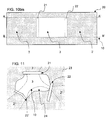
- the figure 11 illustrates an example of a flex-rigid circuit 1 comprising three rigid parts 2, 2 ', 2 "connected by a single flexible portion 3.
- the shape of the blank 10 is any inside the unbonded area 24, 53.
- the figure 12 illustrates another example in which the flexible zone 3 connects four rigid circuits. The cut between the two openings is entirely made on the unglued zone 24, 53.
- the figure 13 represents a 3-terminal flexible portion of circuit board 1. To be terminal, this portion is made from a single window 21. The cutout 10 of the flexible portion is always performed on the unglued portion 24, 53 so that a closed cutting contour (cutout 10 + window 21) of the plate 20 on its unglued portion 24 is made. The portion delimited by this contour is then released leaving the flexible portion 3 free.
- figure 14 illustrates the obtaining of a flex-rigid circuit 1 composed of two strips of several LEDs 4 mounted on an aluminum heat dissipation drain 20.
- figure 14bis illustrates the intermediate structure and the collages and windows provided according to the invention.
- a plurality of pairs of openings 21, 22 is provided to define a plurality of flexible zones 3.
- discontinuous line 10 makes it possible to release each of the shims of the aluminum plate under zones 3.
- the printed circuit manufacturer proceeds according to the steps 100 (initial trimming), 102 (selective adhesive deposition 23) and 104 (application of the flexible substrate 50) described above with reference to FIGS. Figures 2 to 7 .
- the process on the manufacturer's side is continued by an etching step 106a of the copper strip 52 to obtain a printed circuit according to the design desired by the integrator (idem figure 8 ).
- the manufacturer pre-cuts the etched plate as described below with reference to figures 16 and 17 .
- Pre-cutting consists of facilitating the cutting by the final integrator of the still rigid engraved plate without resorting to specific tools. It consists of machined zones 11 arranged to be broken easily, for example by folding. These zones 11 are arranged on all or part of the final cutting path 10 envisaged. In particular, the cutting path 10 at the unglued portion 24, 53 includes some of these zones 11.
- the figure 16 shows a first embodiment in which the printed circuit manufacturer diverts the etched plate along the cutting path 10 leaving some solid areas 11 (the different layers of the etched plate as illustrated by the figure 8 are not represented here). As illustrated on the figure 16a these zones 11 are of small size making it possible to maintain the rigidity of the engraved plate and to be broken under the simple folding force of the two engraved plate parts on either side of the cutting path 10. These zones 11 have a length of several millimeters, generally greater than the width of the trimming performed along the path 10. Several holding and breaking zones 11 are arranged along the path 10, in particular around the unglued zone 53, 24 so as to maintain the part 24 under the rigid substrate 53 for further integration of the components.
- these zones 11 may also be pre-machined so as to provide a groove 12 in V on one side of the plate (bottom of the figure 16b ), preferably on the flexible substrate side, or both sides of the plate (top of the figure 16b ).
- This groove 12 further facilitates breakage by the final integrator.
- the Figures 16c and 16d show that the trimming 10 is traversing so as to separate the aluminum plate and that five rupture zones 11 ensuring the rigidity have been preserved in the example of the cutting path of the figure 16a .
- An alternative to the plurality of zones 11 is to provide the groove or grooves 12 along the cutting path, which is then substantially linear.
- the rupture zones 11 may consist of a plurality of perforations style "postage stamp" for easy manual cutting.
- the solid areas 13 are of small size (much smaller than the width of the trimming) and the perforations 14 of substantially identical size.
- the rigidity is obtained by the succession of the different solid areas 13 on a reduced length L (a few millimeters). It is also possible to machine these zones 11 with one or two V-grooves as illustrated by FIG. figure 16b .
- the etching 106a can be performed after the pre-cutting step 105. In which case, the holding of the wedge 24 to the rest of the plate 20 via the zones 11 greatly facilitates the etching of the flexible zone 53 since the wedge 24 then serves as support.
- the pre-cut etched plate is still rigid thanks to the holding and breaking zones 11. It is delivered by the printed circuit board manufacturer to the electronic circuit integrator.
- the final cutting step 108 is then performed simply by the integrator by breaking, by folding, the rupture zones 11. No cutting equipment is then necessary for the integrator.
- This final cutout 108 allows the removal of the wedge 24 and the release 110 of the flex-rigid circuit 1.
- FIGS 18 and 19 illustrate a flex-rigid printed circuit 1 obtained according to the invention for which the rigid substrate 20 used is provided with a copper face 52 'to form another electric track 5' on the back of the circuit 1.
- the etching step 106, 106a is performed at the same time for the two strips 52 and 52 'to optimize the manufacturing process.
- Silver vias 55 are made in the thickness of the structure obtained to ensure a connection between the different electrical tracks 5, 5 '.
- a current problem with known solutions lies in the fact that rigid circuit parts tend to detach under the effect of vibrations or applied forces. There is therefore a need to improve the fixing of the circuits, in particular flex-rigid circuits 1, to the supports 200.
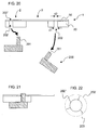
- this problem is solved in the invention by the fact that the rigid substrate is perforated with a registration hole 202 'before the deposition of the flexible substrate 50 and that once the latter deposited, the flexible substrate is also perforated according to the same axis that the registration hole 202 ", the hole 202" made in the flexible substrate having a diameter smaller than that 202 'made in the rigid substrate.
- the portion of the flexible substrate 50 partially obstructing the hole 202' of the rigid substrate 20 deforms to marry the lug 201 and applies a force on the lug 201 which improves the maintenance.
- the holes 202 and lugs 201 are generally cylindrical.
- the diameter d2 of the hole 202 "made in the flexible substrate 50 is between 50 and 95% of the diameter d1 of the hole 202 'made in the rigid substrate 20, preferably 75 to 90%, in particular 80%.
- radial notches 203 are provided on the part of the flexible substrate 50 present at the registration hole 202 'of the rigid substrate 20 (see figure 22 ).
- at least three notches 203 are regularly distributed on the flexible substrate ring delimited by the two perimeters 202 'and 202 ".
Landscapes
- Engineering & Computer Science (AREA)
- Manufacturing & Machinery (AREA)
- Microelectronics & Electronic Packaging (AREA)
- Structure Of Printed Boards (AREA)
- Production Of Multi-Layered Print Wiring Board (AREA)
- Macromolecular Compounds Obtained By Forming Nitrogen-Containing Linkages In General (AREA)
Applications Claiming Priority (1)
| Application Number | Priority Date | Filing Date | Title |
|---|---|---|---|
| FR0705604A FR2919781A1 (fr) | 2007-07-31 | 2007-07-31 | Procede de fabrication d'un circuit imprime semi-flexible, plaque utilisee pour un tel procede, circuit imprime et dispositif electronique associes |
Publications (2)
| Publication Number | Publication Date |
|---|---|
| EP2020833A1 true EP2020833A1 (de) | 2009-02-04 |
| EP2020833B1 EP2020833B1 (de) | 2010-09-22 |
Family
ID=39166402
Family Applications (1)
| Application Number | Title | Priority Date | Filing Date |
|---|---|---|---|
| EP08290744A Not-in-force EP2020833B1 (de) | 2007-07-31 | 2008-07-31 | Herstellungsverfahren für eine starr-flexible Leiterplatte, Brett das für ein solches Verfahren benutzt wird, und damit verbundenen Leiterplatte und elektrischer Gegenstand |
Country Status (4)
| Country | Link |
|---|---|
| EP (1) | EP2020833B1 (de) |
| AT (1) | ATE482609T1 (de) |
| DE (1) | DE602008002655D1 (de) |
| FR (1) | FR2919781A1 (de) |
Cited By (2)
| Publication number | Priority date | Publication date | Assignee | Title |
|---|---|---|---|---|
| EP3754753A1 (de) * | 2019-06-17 | 2020-12-23 | Yazaki Corporation | Sammelschienenmodul |
| CN112654153A (zh) * | 2020-11-12 | 2021-04-13 | 惠州市金百泽电路科技有限公司 | 一种测控设备高精度光波标尺pcb的加工方法 |
Families Citing this family (1)
| Publication number | Priority date | Publication date | Assignee | Title |
|---|---|---|---|---|
| US20200053887A1 (en) | 2018-08-09 | 2020-02-13 | At&S Austria Technologie & Systemtechnik Aktiengesellschaft | Mechanically Robust Component Carrier With Rigid and Flexible Portions |
Citations (16)
| Publication number | Priority date | Publication date | Assignee | Title |
|---|---|---|---|---|
| DE2914336A1 (de) * | 1979-04-09 | 1980-11-06 | Telefonbau & Normalzeit Gmbh | Verfahren zur herstellung starr- flexibler leiterplatten |
| GB2063571A (en) * | 1979-11-20 | 1981-06-03 | Kollmorgen Tech Corp | Circuit boards |
| EP0126856A2 (de) * | 1983-05-21 | 1984-12-05 | GRUNDIG E.M.V. Elektro-Mechanische Versuchsanstalt Max Grundig holländ. Stiftung & Co. KG. | Verfahren zum Herstellen von Leiterplatten mit starren und flexiblen Bereichen |
| DE3417223A1 (de) * | 1984-05-10 | 1985-11-21 | Hans 6052 Mühlheim Keller | Verfahren zur herstellung einer mehrfachnutzenkopie fuer gedruckte schaltungen und vorrichtung zur durchfuehrung des verfahrens |
| EP0175045A2 (de) * | 1984-09-21 | 1986-03-26 | Firma Carl Freudenberg | Verfahren zur Herstellung von durchkontaktierten flexiblen Leiterplatten für hohe Biegebeanspruchung |
| EP0195935A2 (de) * | 1985-03-27 | 1986-10-01 | PPC Electronic AG | Verfahren zur Herstellung einer starre und flexible Partien aufweisenden Leiterplatte für gedruckte elektrische Schaltungen |
| EP0440928A2 (de) * | 1990-02-05 | 1991-08-14 | Firma Carl Freudenberg | Verfahren zur Herstellung einer starre und flexible Bereiche aufweisenden Leiterplatte |
| DE4208610C1 (en) * | 1992-03-18 | 1993-05-19 | Fa. Carl Freudenberg, 6940 Weinheim, De | Rigid-flexible PCB with flexible circuit foil mfg. - having flexible PCB in flexible region with fracture lines in rigid outer layers along rigid-flexible transition allowing rigid part to be removed along fracture lines after processing |
| DE4206746C1 (en) * | 1992-03-04 | 1993-06-24 | Degussa Ag, 6000 Frankfurt, De | Manufacture of circuit board with rigid and flexible sections - has flexible sections created by having non-bonding insert of insulation broken away |
| EP0776596B1 (de) * | 1994-08-02 | 2001-10-24 | Coesen, Inc. | Starr-flexible leiterplatte |
| US6687984B1 (en) * | 1999-07-19 | 2004-02-10 | Nippon Mektron, Ltd. | Method for manufacturing flexible multilayer circuit board |
| US20040118595A1 (en) * | 2002-12-06 | 2004-06-24 | Flammer Jeffrey D. | Rigid-flex circuit board system |
| FR2871334A1 (fr) | 2004-06-03 | 2005-12-09 | Bree Beauce Realisations Et Et | Circuit imprime semi-flexible |
| FR2871336A1 (fr) | 2004-06-02 | 2005-12-09 | Bree Ind Soc Par Actions Simpl | Circuit imprime flex-rigide par collage |
| US20060231198A1 (en) * | 2005-03-15 | 2006-10-19 | Vasoya Kalu K | Manufacturing process: how to construct constraining core material into printed wiring board |
| US7234230B1 (en) * | 2005-12-27 | 2007-06-26 | Gold Circuit Electronics Ltd. | Composite circuit board and method for manufacturing the same |
-
2007
- 2007-07-31 FR FR0705604A patent/FR2919781A1/fr not_active Withdrawn
-
2008
- 2008-07-31 DE DE602008002655T patent/DE602008002655D1/de active Active
- 2008-07-31 AT AT08290744T patent/ATE482609T1/de not_active IP Right Cessation
- 2008-07-31 EP EP08290744A patent/EP2020833B1/de not_active Not-in-force
Patent Citations (16)
| Publication number | Priority date | Publication date | Assignee | Title |
|---|---|---|---|---|
| DE2914336A1 (de) * | 1979-04-09 | 1980-11-06 | Telefonbau & Normalzeit Gmbh | Verfahren zur herstellung starr- flexibler leiterplatten |
| GB2063571A (en) * | 1979-11-20 | 1981-06-03 | Kollmorgen Tech Corp | Circuit boards |
| EP0126856A2 (de) * | 1983-05-21 | 1984-12-05 | GRUNDIG E.M.V. Elektro-Mechanische Versuchsanstalt Max Grundig holländ. Stiftung & Co. KG. | Verfahren zum Herstellen von Leiterplatten mit starren und flexiblen Bereichen |
| DE3417223A1 (de) * | 1984-05-10 | 1985-11-21 | Hans 6052 Mühlheim Keller | Verfahren zur herstellung einer mehrfachnutzenkopie fuer gedruckte schaltungen und vorrichtung zur durchfuehrung des verfahrens |
| EP0175045A2 (de) * | 1984-09-21 | 1986-03-26 | Firma Carl Freudenberg | Verfahren zur Herstellung von durchkontaktierten flexiblen Leiterplatten für hohe Biegebeanspruchung |
| EP0195935A2 (de) * | 1985-03-27 | 1986-10-01 | PPC Electronic AG | Verfahren zur Herstellung einer starre und flexible Partien aufweisenden Leiterplatte für gedruckte elektrische Schaltungen |
| EP0440928A2 (de) * | 1990-02-05 | 1991-08-14 | Firma Carl Freudenberg | Verfahren zur Herstellung einer starre und flexible Bereiche aufweisenden Leiterplatte |
| DE4206746C1 (en) * | 1992-03-04 | 1993-06-24 | Degussa Ag, 6000 Frankfurt, De | Manufacture of circuit board with rigid and flexible sections - has flexible sections created by having non-bonding insert of insulation broken away |
| DE4208610C1 (en) * | 1992-03-18 | 1993-05-19 | Fa. Carl Freudenberg, 6940 Weinheim, De | Rigid-flexible PCB with flexible circuit foil mfg. - having flexible PCB in flexible region with fracture lines in rigid outer layers along rigid-flexible transition allowing rigid part to be removed along fracture lines after processing |
| EP0776596B1 (de) * | 1994-08-02 | 2001-10-24 | Coesen, Inc. | Starr-flexible leiterplatte |
| US6687984B1 (en) * | 1999-07-19 | 2004-02-10 | Nippon Mektron, Ltd. | Method for manufacturing flexible multilayer circuit board |
| US20040118595A1 (en) * | 2002-12-06 | 2004-06-24 | Flammer Jeffrey D. | Rigid-flex circuit board system |
| FR2871336A1 (fr) | 2004-06-02 | 2005-12-09 | Bree Ind Soc Par Actions Simpl | Circuit imprime flex-rigide par collage |
| FR2871334A1 (fr) | 2004-06-03 | 2005-12-09 | Bree Beauce Realisations Et Et | Circuit imprime semi-flexible |
| US20060231198A1 (en) * | 2005-03-15 | 2006-10-19 | Vasoya Kalu K | Manufacturing process: how to construct constraining core material into printed wiring board |
| US7234230B1 (en) * | 2005-12-27 | 2007-06-26 | Gold Circuit Electronics Ltd. | Composite circuit board and method for manufacturing the same |
Cited By (3)
| Publication number | Priority date | Publication date | Assignee | Title |
|---|---|---|---|---|
| EP3754753A1 (de) * | 2019-06-17 | 2020-12-23 | Yazaki Corporation | Sammelschienenmodul |
| US11646458B2 (en) | 2019-06-17 | 2023-05-09 | Yazaki Corporation | Busbar module |
| CN112654153A (zh) * | 2020-11-12 | 2021-04-13 | 惠州市金百泽电路科技有限公司 | 一种测控设备高精度光波标尺pcb的加工方法 |
Also Published As
| Publication number | Publication date |
|---|---|
| DE602008002655D1 (de) | 2010-11-04 |
| FR2919781A1 (fr) | 2009-02-06 |
| EP2020833B1 (de) | 2010-09-22 |
| ATE482609T1 (de) | 2010-10-15 |
Similar Documents
| Publication | Publication Date | Title |
|---|---|---|
| EP0913076B1 (de) | Verfahren zur herstellung von gedruckten schaltungen sowie nach diesem verfahren hergestellte gedruckte schaltung | |
| EP3005846B1 (de) | Verfahren zur herstellung einer bestückten schaltung | |
| EP1634685A2 (de) | Dünner elektronischer Chip auf Glas für elektronisches Bauelement und Herstellungsverfahren | |
| KR20070081422A (ko) | 배선 기판의 제조 방법 | |
| SE515856C2 (sv) | Bärare för elektronikkomponenter | |
| JP5693468B2 (ja) | 少なくとも1つのレーザビームストップ素子を有するプリント基板素子ならびにプリント基板素子を作製する方法 | |
| US7377030B2 (en) | Wiring board manufacturing method | |
| EP2020833B1 (de) | Herstellungsverfahren für eine starr-flexible Leiterplatte, Brett das für ein solches Verfahren benutzt wird, und damit verbundenen Leiterplatte und elektrischer Gegenstand | |
| EP0044247B1 (de) | Verfahren zur Herstellung eines Trägers für elektronische Elemente zur Verbindung integrierter Halbleiteranordnungen | |
| CN103068189A (zh) | 制造多层电路板的方法以及多层电路板 | |
| EP1457101B1 (de) | Verfahren zur herstellung eines mehrschichtigen moduls mit hochdichten gedruckten schaltungen | |
| FR2635920A1 (fr) | Procede de fabrication d'une zone de connexion pour un circuit hyperfrequence de type triplaque et circuit ainsi obtenu | |
| EP3932152B1 (de) | Elektronikkarte mit bestandteilen in höhlen und gemeinsamen lötungsbereichen | |
| FR2822338A1 (fr) | Procede pour connecter electriquement des plots de contact d'un composant microelectronique directement a des pistes de circuits imprimes, et plaque a circuits imprimes ainsi constituee | |
| EP2866173B1 (de) | Verfahren zur Erzeugung eines elektrischen Schaltkreises, und mit diesem Verfahren erzeugter Schaltkreis | |
| FR2965139A1 (fr) | Support de circuit et procede de fabrication d'un tel support de circuit | |
| EP4280828A1 (de) | Verbesserte elektrische verbindung zwischen einer flex-schaltung und einer starren schaltung, entsprechender anschlussstift | |
| WO2021219630A1 (fr) | Procede de fabrication d'une carte a puce comportant du bois et conforme au standard des cartes a puce | |
| EP3171395B1 (de) | Herstellung von verbindungen durch umbiegen von leiterelementen unter eine mikroelektronische vorrichtung wie einen chip | |
| FR2983149A1 (fr) | Plaque mixte | |
| FR3101748A1 (fr) | Procédé de fabrication d’un circuit imprimé et circuit imprimé | |
| EP2205053B1 (de) | Gedruckte Schaltkreiskarte und Verfahren für dessen Herstellung | |
| US20240049397A1 (en) | Methods to fill through-holes of a substrate with metal paste | |
| EP2862424B1 (de) | Verfahren zur herstellung einer elektronischen schaltung mit schutz der leitenden schicht | |
| FR3093270A1 (fr) | Superposition de composants électroniques avec insertion dans des cavités |
Legal Events
| Date | Code | Title | Description |
|---|---|---|---|
| PUAI | Public reference made under article 153(3) epc to a published international application that has entered the european phase |
Free format text: ORIGINAL CODE: 0009012 |
|
| AK | Designated contracting states |
Kind code of ref document: A1 Designated state(s): AT BE BG CH CY CZ DE DK EE ES FI FR GB GR HR HU IE IS IT LI LT LU LV MC MT NL NO PL PT RO SE SI SK TR |
|
| AX | Request for extension of the european patent |
Extension state: AL BA MK RS |
|
| 17P | Request for examination filed |
Effective date: 20090723 |
|
| AKX | Designation fees paid |
Designated state(s): AT BE BG CH CY CZ DE DK EE ES FI FR GB GR HR HU IE IS IT LI LT LU LV MC MT NL NO PL PT RO SE SI SK TR |
|
| 17Q | First examination report despatched |
Effective date: 20091001 |
|
| GRAP | Despatch of communication of intention to grant a patent |
Free format text: ORIGINAL CODE: EPIDOSNIGR1 |
|
| GRAS | Grant fee paid |
Free format text: ORIGINAL CODE: EPIDOSNIGR3 |
|
| GRAA | (expected) grant |
Free format text: ORIGINAL CODE: 0009210 |
|
| AK | Designated contracting states |
Kind code of ref document: B1 Designated state(s): AT BE BG CH CY CZ DE DK EE ES FI FR GB GR HR HU IE IS IT LI LT LU LV MC MT NL NO PL PT RO SE SI SK TR |
|
| REG | Reference to a national code |
Ref country code: GB Ref legal event code: FG4D Free format text: NOT ENGLISH |
|
| REG | Reference to a national code |
Ref country code: CH Ref legal event code: EP |
|
| REG | Reference to a national code |
Ref country code: IE Ref legal event code: FG4D Free format text: LANGUAGE OF EP DOCUMENT: FRENCH |
|
| REF | Corresponds to: |
Ref document number: 602008002655 Country of ref document: DE Date of ref document: 20101104 Kind code of ref document: P |
|
| PG25 | Lapsed in a contracting state [announced via postgrant information from national office to epo] |
Ref country code: FI Free format text: LAPSE BECAUSE OF FAILURE TO SUBMIT A TRANSLATION OF THE DESCRIPTION OR TO PAY THE FEE WITHIN THE PRESCRIBED TIME-LIMIT Effective date: 20100922 Ref country code: NO Free format text: LAPSE BECAUSE OF FAILURE TO SUBMIT A TRANSLATION OF THE DESCRIPTION OR TO PAY THE FEE WITHIN THE PRESCRIBED TIME-LIMIT Effective date: 20101222 Ref country code: LT Free format text: LAPSE BECAUSE OF FAILURE TO SUBMIT A TRANSLATION OF THE DESCRIPTION OR TO PAY THE FEE WITHIN THE PRESCRIBED TIME-LIMIT Effective date: 20100922 Ref country code: AT Free format text: LAPSE BECAUSE OF FAILURE TO SUBMIT A TRANSLATION OF THE DESCRIPTION OR TO PAY THE FEE WITHIN THE PRESCRIBED TIME-LIMIT Effective date: 20100922 |
|
| REG | Reference to a national code |
Ref country code: NL Ref legal event code: VDEP Effective date: 20100922 |
|
| LTIE | Lt: invalidation of european patent or patent extension |
Effective date: 20100922 |
|
| PG25 | Lapsed in a contracting state [announced via postgrant information from national office to epo] |
Ref country code: HR Free format text: LAPSE BECAUSE OF FAILURE TO SUBMIT A TRANSLATION OF THE DESCRIPTION OR TO PAY THE FEE WITHIN THE PRESCRIBED TIME-LIMIT Effective date: 20100922 Ref country code: PL Free format text: LAPSE BECAUSE OF FAILURE TO SUBMIT A TRANSLATION OF THE DESCRIPTION OR TO PAY THE FEE WITHIN THE PRESCRIBED TIME-LIMIT Effective date: 20100922 Ref country code: SI Free format text: LAPSE BECAUSE OF FAILURE TO SUBMIT A TRANSLATION OF THE DESCRIPTION OR TO PAY THE FEE WITHIN THE PRESCRIBED TIME-LIMIT Effective date: 20100922 |
|
| PG25 | Lapsed in a contracting state [announced via postgrant information from national office to epo] |
Ref country code: GR Free format text: LAPSE BECAUSE OF FAILURE TO SUBMIT A TRANSLATION OF THE DESCRIPTION OR TO PAY THE FEE WITHIN THE PRESCRIBED TIME-LIMIT Effective date: 20101223 Ref country code: SE Free format text: LAPSE BECAUSE OF FAILURE TO SUBMIT A TRANSLATION OF THE DESCRIPTION OR TO PAY THE FEE WITHIN THE PRESCRIBED TIME-LIMIT Effective date: 20100922 Ref country code: LV Free format text: LAPSE BECAUSE OF FAILURE TO SUBMIT A TRANSLATION OF THE DESCRIPTION OR TO PAY THE FEE WITHIN THE PRESCRIBED TIME-LIMIT Effective date: 20100922 |
|
| REG | Reference to a national code |
Ref country code: IE Ref legal event code: FD4D |
|
| PG25 | Lapsed in a contracting state [announced via postgrant information from national office to epo] |
Ref country code: IE Free format text: LAPSE BECAUSE OF FAILURE TO SUBMIT A TRANSLATION OF THE DESCRIPTION OR TO PAY THE FEE WITHIN THE PRESCRIBED TIME-LIMIT Effective date: 20100922 |
|
| PG25 | Lapsed in a contracting state [announced via postgrant information from national office to epo] |
Ref country code: SK Free format text: LAPSE BECAUSE OF FAILURE TO SUBMIT A TRANSLATION OF THE DESCRIPTION OR TO PAY THE FEE WITHIN THE PRESCRIBED TIME-LIMIT Effective date: 20100922 Ref country code: IS Free format text: LAPSE BECAUSE OF FAILURE TO SUBMIT A TRANSLATION OF THE DESCRIPTION OR TO PAY THE FEE WITHIN THE PRESCRIBED TIME-LIMIT Effective date: 20110122 Ref country code: CZ Free format text: LAPSE BECAUSE OF FAILURE TO SUBMIT A TRANSLATION OF THE DESCRIPTION OR TO PAY THE FEE WITHIN THE PRESCRIBED TIME-LIMIT Effective date: 20100922 Ref country code: EE Free format text: LAPSE BECAUSE OF FAILURE TO SUBMIT A TRANSLATION OF THE DESCRIPTION OR TO PAY THE FEE WITHIN THE PRESCRIBED TIME-LIMIT Effective date: 20100922 Ref country code: RO Free format text: LAPSE BECAUSE OF FAILURE TO SUBMIT A TRANSLATION OF THE DESCRIPTION OR TO PAY THE FEE WITHIN THE PRESCRIBED TIME-LIMIT Effective date: 20100922 Ref country code: NL Free format text: LAPSE BECAUSE OF FAILURE TO SUBMIT A TRANSLATION OF THE DESCRIPTION OR TO PAY THE FEE WITHIN THE PRESCRIBED TIME-LIMIT Effective date: 20100922 Ref country code: IT Free format text: LAPSE BECAUSE OF FAILURE TO SUBMIT A TRANSLATION OF THE DESCRIPTION OR TO PAY THE FEE WITHIN THE PRESCRIBED TIME-LIMIT Effective date: 20100922 Ref country code: PT Free format text: LAPSE BECAUSE OF FAILURE TO SUBMIT A TRANSLATION OF THE DESCRIPTION OR TO PAY THE FEE WITHIN THE PRESCRIBED TIME-LIMIT Effective date: 20110124 |
|
| PG25 | Lapsed in a contracting state [announced via postgrant information from national office to epo] |
Ref country code: ES Free format text: LAPSE BECAUSE OF FAILURE TO SUBMIT A TRANSLATION OF THE DESCRIPTION OR TO PAY THE FEE WITHIN THE PRESCRIBED TIME-LIMIT Effective date: 20110102 |
|
| PLBE | No opposition filed within time limit |
Free format text: ORIGINAL CODE: 0009261 |
|
| STAA | Information on the status of an ep patent application or granted ep patent |
Free format text: STATUS: NO OPPOSITION FILED WITHIN TIME LIMIT |
|
| 26N | No opposition filed |
Effective date: 20110623 |
|
| PG25 | Lapsed in a contracting state [announced via postgrant information from national office to epo] |
Ref country code: DK Free format text: LAPSE BECAUSE OF FAILURE TO SUBMIT A TRANSLATION OF THE DESCRIPTION OR TO PAY THE FEE WITHIN THE PRESCRIBED TIME-LIMIT Effective date: 20100922 |
|
| REG | Reference to a national code |
Ref country code: DE Ref legal event code: R097 Ref document number: 602008002655 Country of ref document: DE Effective date: 20110623 |
|
| PG25 | Lapsed in a contracting state [announced via postgrant information from national office to epo] |
Ref country code: MT Free format text: LAPSE BECAUSE OF FAILURE TO SUBMIT A TRANSLATION OF THE DESCRIPTION OR TO PAY THE FEE WITHIN THE PRESCRIBED TIME-LIMIT Effective date: 20100922 |
|
| BERE | Be: lapsed |
Owner name: BEAUCE REALISATIONS ET ETUDES ELECTRONIQUES (BREE) Effective date: 20110731 |
|
| PG25 | Lapsed in a contracting state [announced via postgrant information from national office to epo] |
Ref country code: MC Free format text: LAPSE BECAUSE OF NON-PAYMENT OF DUE FEES Effective date: 20110731 |
|
| REG | Reference to a national code |
Ref country code: FR Ref legal event code: ST Effective date: 20120330 |
|
| PG25 | Lapsed in a contracting state [announced via postgrant information from national office to epo] |
Ref country code: FR Free format text: LAPSE BECAUSE OF NON-PAYMENT OF DUE FEES Effective date: 20110801 Ref country code: BE Free format text: LAPSE BECAUSE OF NON-PAYMENT OF DUE FEES Effective date: 20110731 |
|
| REG | Reference to a national code |
Ref country code: CH Ref legal event code: PL |
|
| GBPC | Gb: european patent ceased through non-payment of renewal fee |
Effective date: 20120731 |
|
| PG25 | Lapsed in a contracting state [announced via postgrant information from national office to epo] |
Ref country code: LI Free format text: LAPSE BECAUSE OF NON-PAYMENT OF DUE FEES Effective date: 20120731 Ref country code: GB Free format text: LAPSE BECAUSE OF NON-PAYMENT OF DUE FEES Effective date: 20120731 Ref country code: CH Free format text: LAPSE BECAUSE OF NON-PAYMENT OF DUE FEES Effective date: 20120731 |
|
| PG25 | Lapsed in a contracting state [announced via postgrant information from national office to epo] |
Ref country code: CY Free format text: LAPSE BECAUSE OF EXPIRATION OF PROTECTION Effective date: 20100922 Ref country code: LU Free format text: LAPSE BECAUSE OF NON-PAYMENT OF DUE FEES Effective date: 20110731 |
|
| PG25 | Lapsed in a contracting state [announced via postgrant information from national office to epo] |
Ref country code: TR Free format text: LAPSE BECAUSE OF FAILURE TO SUBMIT A TRANSLATION OF THE DESCRIPTION OR TO PAY THE FEE WITHIN THE PRESCRIBED TIME-LIMIT Effective date: 20100922 Ref country code: BG Free format text: LAPSE BECAUSE OF FAILURE TO SUBMIT A TRANSLATION OF THE DESCRIPTION OR TO PAY THE FEE WITHIN THE PRESCRIBED TIME-LIMIT Effective date: 20101222 |
|
| PG25 | Lapsed in a contracting state [announced via postgrant information from national office to epo] |
Ref country code: HU Free format text: LAPSE BECAUSE OF FAILURE TO SUBMIT A TRANSLATION OF THE DESCRIPTION OR TO PAY THE FEE WITHIN THE PRESCRIBED TIME-LIMIT Effective date: 20100922 |
|
| PGFP | Annual fee paid to national office [announced via postgrant information from national office to epo] |
Ref country code: DE Payment date: 20140724 Year of fee payment: 7 |
|
| REG | Reference to a national code |
Ref country code: DE Ref legal event code: R119 Ref document number: 602008002655 Country of ref document: DE |
|
| PG25 | Lapsed in a contracting state [announced via postgrant information from national office to epo] |
Ref country code: DE Free format text: LAPSE BECAUSE OF NON-PAYMENT OF DUE FEES Effective date: 20160202 |