EP2023389A2 - Dissipateur de chaleur intégré pour modules semi-conducteurs - Google Patents
Dissipateur de chaleur intégré pour modules semi-conducteurs Download PDFInfo
- Publication number
- EP2023389A2 EP2023389A2 EP08161714A EP08161714A EP2023389A2 EP 2023389 A2 EP2023389 A2 EP 2023389A2 EP 08161714 A EP08161714 A EP 08161714A EP 08161714 A EP08161714 A EP 08161714A EP 2023389 A2 EP2023389 A2 EP 2023389A2
- Authority
- EP
- European Patent Office
- Prior art keywords
- semiconductor module
- frame part
- reinforcing beam
- semiconductor
- semiconductor device
- Prior art date
- Legal status (The legal status is an assumption and is not a legal conclusion. Google has not performed a legal analysis and makes no representation as to the accuracy of the status listed.)
- Granted
Links
Images




Classifications
-
- H—ELECTRICITY
- H05—ELECTRIC TECHNIQUES NOT OTHERWISE PROVIDED FOR
- H05K—PRINTED CIRCUITS; CASINGS OR CONSTRUCTIONAL DETAILS OF ELECTRIC APPARATUS; MANUFACTURE OF ASSEMBLAGES OF ELECTRICAL COMPONENTS
- H05K7/00—Constructional details common to different types of electric apparatus
- H05K7/20—Modifications to facilitate cooling, ventilating, or heating
- H05K7/2039—Modifications to facilitate cooling, ventilating, or heating characterised by the heat transfer by conduction from the heat generating element to a dissipating body
- H05K7/20436—Inner thermal coupling elements in heat dissipating housings, e.g. protrusions or depressions integrally formed in the housing
- H05K7/2049—Pressing means used to urge contact, e.g. springs
-
- H—ELECTRICITY
- H10—SEMICONDUCTOR DEVICES; ELECTRIC SOLID-STATE DEVICES NOT OTHERWISE PROVIDED FOR
- H10W—GENERIC PACKAGES, INTERCONNECTIONS, CONNECTORS OR OTHER CONSTRUCTIONAL DETAILS OF DEVICES COVERED BY CLASS H10
- H10W40/00—Arrangements for thermal protection or thermal control
- H10W40/60—Securing means for detachable heating or cooling arrangements, e.g. clamps
-
- H—ELECTRICITY
- H10—SEMICONDUCTOR DEVICES; ELECTRIC SOLID-STATE DEVICES NOT OTHERWISE PROVIDED FOR
- H10W—GENERIC PACKAGES, INTERCONNECTIONS, CONNECTORS OR OTHER CONSTRUCTIONAL DETAILS OF DEVICES COVERED BY CLASS H10
- H10W72/00—Interconnections or connectors in packages
-
- H—ELECTRICITY
- H10—SEMICONDUCTOR DEVICES; ELECTRIC SOLID-STATE DEVICES NOT OTHERWISE PROVIDED FOR
- H10W—GENERIC PACKAGES, INTERCONNECTIONS, CONNECTORS OR OTHER CONSTRUCTIONAL DETAILS OF DEVICES COVERED BY CLASS H10
- H10W76/00—Containers; Fillings or auxiliary members therefor; Seals
- H10W76/40—Fillings or auxiliary members in containers, e.g. centering rings
Definitions
- This invention relates to a semiconductor device provided with a semiconductor module that is mounted on a mobile object such as a vehicle, the invention contributing particularly to a reduction in influence of a thermal stress due to heating.
- a conventional semiconductor device is generally provided with a semiconductor module having a semiconductor element sealed with a resin and a screw through-hole provided at a central part thereof, a plate-like presser spring disposed at one side of the semiconductor module, a reinforcing beam for reinforcing the presser plate-like spring, and a heatsink disposed at the other side of the semiconductor module, wherein the semiconductor module is fixed to the heatsink by a screw inserted from the reinforcing beam side into the screw through-hole of the semiconductor module via the reinforcing beam and the presser plate-like spring, and the presser plate-like spring has a slit formed for dividing a peripheral part thereof (see Patent Publication 1, for example).
- Patent Publication 1 JP-A-2005-235 992 (Paragraph [0005], Fig. 1 , etc.)
- the conventional semiconductor device is formed by fixing the members such as the semiconductor module, the plate-like spring, and the reinforcing beam to the heatsink.
- the heat generated in the semiconductor module is discharged to the heatsink, and the heat transferred to the heatsink is discharged to the outside via a cooling member attached to a reverse surface (a surface reverse to a surface on which the semiconductor module is attached).
- a thermally conductive member in the form of a paste or a flexible sheet is generally provided between the semiconductor module and the heatsink and between the heatsink and the cooling member for suppressing heat resistance.
- the semiconductor device has a difficulty in stably exhibiting the original performance since the deformation of the heatsink is subject to various factors such as influences of the pressing force by the reinforcing beam and the plate-like spring, influence of the pressure contact force for keeping the thermally conductive member thin and uniform, and influence of the thermal stress caused by a use environment temperature of the semiconductor device and the heat generation in the semiconductor module.
- the present invention has been made to solve the above-described problems, and an object thereof is to obtain a semiconductor device that is reduced in size, weight, and cost and improved in performance stability and productivity.
- the semiconductor device of this invention comprises: a semiconductor module in which a semiconductor element is sealed with a resin; a reinforcing beam fixed to an upper surface of the semiconductor module; and a frame part to which the reinforcing beam is fixed, the frame part being disposed in such a fashion as to enclose an outer periphery of the semiconductor module and the reinforcing beam fixed to the semiconductor module.
- any heatsink is unnecessary, thereby achieving the desired reductions in size, weight, and cost of the semiconductor device. Also, since a heatsink is unnecessary, it is possible to discharge heat generated in the semiconductor module directly to a cooling member as well as to suppress thermal resistance, thereby enabling the semiconductor to stably exhibit its performance.
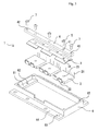
- Fig. 1 is a broken perspective view showing a structure of a semiconductor device according to Embodiment 1 of this invention.
- Fig. 2 is a perspective view showing a state in which the semiconductor device of Fig. 1 is assembled.
- Fig. 3 is a sectional view showing a part of the semiconductor device of Fig. 2 , wherein a frame part is omitted.
- Fig. 4 is a schematic diagram showing one example of fixing a cooling member and a control unit to the semiconductor device of Fig. 2 .
- a semiconductor device 1 is provided with semiconductor modules 2 in which semiconductor elements are sealed with a resin, a reinforcing beam 4 fixed to an upper surface of the semiconductor module 2 via a plate-like spring 3, a frame part 6 disposed in such a fashion as to enclose the semiconductor module 2, the plate-like spring 3, and the reinforcing beam 4, the reinforcing beam 4 having its both ends fixed to the frame part 6.
- the semiconductor modules 2 are provided with control terminals 21 connected to a control unit described later in this specification and terminals 22 for connection to connection terminals that are provided at the frame part and described later in this specification.
- a screw hole 23 is provided at a central part of the semiconductor module 2, for fixing the plate-like spring 3 and the reinforcing beam 4.
- Embodiment 1 three semiconductor modules 2 are disposed in line at a predetermined interval, and the plate-like spring 3 of which a part at a position corresponding to each of the semiconductor modules 2 is formed into a pentroof type sectional shape is disposed on the upper surface of each of the semiconductor modules 2. Also, a fixing hole 31 is provided at a position on the plate-like spring 3 corresponding to the screw hole 23 of the semiconductor module 2.
- the reinforcing beam 4 extending in a direction in which the semiconductor modules 2 are disposed, i.e. along a length direction of the plate-like spring 3, is disposed, and through-holes 41 are provided corresponding to the interval at which the three semiconductor modules 2 are disposed.
- a fixing hole 42 for the fixation to the frame part 6 is provided at each of the both ends of the reinforcing beam 4.
- the reinforcing beam 4, the plate-like spring 3, and the semiconductor modules 2 are fixed to one another by a screw 5 inserted as a first fastening tool from above the reinforcing beam 4 into the through-hole 41, the hole 31, and the screw hole 23 in this order.
- the fastening force of the screw 5 is distributed by flexure of a part of the pentroof type sectional shape of the plate-like spring 3, so that a uniform load is applied on the semiconductor module 2 when the plate-like spring 3 is fixed as being perfectly spread.
- a nut may be formed inside the semiconductor module 2 by insertion molding when there is a risk of cracking in the resin or when a high fastening force is required.
- the fixing method is not limited to the above, and the members may be fixed by providing a through-hole in the semiconductor module 2 in place of the screw hole 23, disposing a nut on a lower surface of the semiconductor module 2, and fastening the screw 5 with the nut, for example.
- the members may be fixed by providing a through-hole in the semiconductor module 2 in place of the screw hole 23, providing a screw hole in the reinforcing beam 4 in place of the through-hole 41, and inserting the screw from the lower surface of the semiconductor module 2.
- thread-cutting on the semiconductor module 2 is unnecessary, and it is possible to prevent rupture of the semiconductor module 2 otherwise caused by a crack or the like in the screw hole 23.
- the frame part 6 is formed in the form of a frame in such a fashion as to enclose from four directions the reinforcing beam 4, the plate-like spring 3, and the semiconductor module 2 that are integrally fixed to one another.
- a step part 61 is projecting from each of opposite inner walls in a width direction of the frame part 6 for fixing the reinforcing beam 4, and a screw hole 62 is provided at a central part of the step part 61.
- the reinforcing beam 4 is disposed in such a fashion that the fixing hole 42 of the reinforcing beam 4 overlaps with the screw hole 62, so that the reinforcing beam 4 and the frame part 6 are fixed to each other when a screw 7 serving as a second fixing tool is inserted from the side of the reinforcing beam 4 to be fastened in the screw hole 62.
- the semiconductor module 2, the plate-like spring 3, the reinforcing beam 4, and the frame part 6 are integrally fixed to form the semiconductor device 1.
- the reinforcing beam 4 is fixed to the frame part 6 in Embodiment 1, this invention is not limited thereto, and the plate-like spring 3 may be fixed to the frame part 6 together with the reinforcing beam 4 by extending both ends in the length direction of the plate-like spring 3.
- Jutting parts 64 in which fixing holes 63 for fixing onto the cooling member described later in this specification are disposed are formed on each of both outer wall surfaces in the length direction of the frame part 6.
- Support parts 65 for fixing and supporting the control unit described later in this specification are provided at each of four corners of an upper surface of a framing part of the frame part 6.
- thermoplastic synthetic resin material such as ABS, PBT, and PPS may be used as a material for the frame part 6, and the frame part 6 may be shaped by injection molding.
- connection terminal 66a One end of the bus bar 66 is exposed to an inner wall side of the frame part 6 as a connection terminal 66a to be connected to the terminal 22 of the semiconductor module 2, and the other end is exposed to an outer wall side of the frame part 6 as an external terminal 66b to be connected to an external component.
- the terminal 22 and the connection terminal 66a are connected by welding, for example, to form a desired electric circuit.
- the connection method is not limited to the welding, and the connection may be established by fastening with a screw.
- thicknesses of the semiconductor module 2, the frame part 6, the step part 61, and the like are so set that positions of the lower surface of the semiconductor module 2 and the lower surface of the frame part 6 are on an identical plane when the members (semiconductor module 2, plate-like spring 3, reinforcing beam 4, frame part 6) are integrally fixed. With such a constitution, the cooling member described later in this specification and the lower surface of the semiconductor module 2 are reliably brought into contact with each other.
- FIG. 4 The schematic diagram of Fig. 4 is a diagram as viewed from a side of the semiconductor device 1 shown in Fig. 2 in the width direction.
- the cooling member 80 is disposed at a side of the lower surface of the semiconductor device 1 and used for discharging heat generated in the semiconductor module 2 by contacting the lower surface of the semiconductor module 2.
- a screw hole 81 is provided on the cooling member 80 at a position corresponding to the fixing hole 63 provided on the respective jutting part 64 of the frame part 6.
- the cooling member 80 is disposed below the frame part 6 in such a fashion as to be in contact with the lower surface of the semiconductor module 2, and a screw is fastened in the screw hole 81 of the cooling member 80 via the fixing hole 63, so that the frame part 6 and the cooling member 80 are fixed to each other.
- the fixing method of the frame member 6 and the cooling member 80 is not limited to the above, and the frame member 6 and the cooling member 80 are fixed in accordance with use conditions and the like of the semiconductor device 1.
- a thermally conductive member 82 (see Fig. 4 ) having a thermal conductivity ratio of about 1 W/mK to several W/mK and in the form of a paste or a flexible sheet is provided between the semiconductor module 2 and the cooling member 80 by coating, sandwiching, or the like.
- the thermally conductive member 82 allows smooth thermal conduction by closely contacting a contact surface between the semiconductor module 2 and the cooling member 80.
- a heat discharge effect of the thermally conductive member 82 is increased as the thickness thereof is reduced, but heat resistance of a part having a relatively large thickness is increased when the thickness is increased and non-uniform.
- the thermally conductive member 82 Since performance of the thermally conducive member 82 is limited to the part having the larger heat resistance, the thermally conductive member 82 can be the major factor of deterioration of heat resistance when the thermally conductive member 82 is not used appropriately. Therefore, it is desirable to keep the thickness of the thermally conductive member 82 small and uniform by increasing a pressure contact force between the semiconductor module 2 and the cooling member 80.
- the pressure contact force depends on rigidity of the reinforcing beam 4. Therefore, by using an iron-based material having a high Young's modulus as a material for the reinforcing beam 4, it is possible to more reliably prevent the reinforcing beam 4 from being deformed and the like when the pressure contact force is increased.
- a rib for example, passing between the semiconductor modules 2 may be provided in the length direction of the frame part 6 for further suppressing the reinforcing beam 4 from being deformed.
- a force of pressing the central semiconductor module 2 among the three semiconductor modules 2 can be weakened as compared to those of the semiconductor modules 2 on both ends when the reinforcing beam 4 is slightly deformed depending on the rigidity of the reinforcing beam 4.
- the deformation amount of the central spring is increased by increasing an angle of an inclined part of the pentroof type section, thereby increasing the pressing force for the semiconductor module 2.
- the deformation amount of the spring may be changed by changing a spring constant of the plate-like spring 3.
- a recessed part is provided on the cooling member 80 at a part corresponding to the jutting part of the nut.
- the control unit 83 (see Fig. 4 ) is disposed above the frame part 6, for example, for driving and controlling the semiconductor module 2.
- through-holes 84 are provided in the control unit 83 at each of positions corresponding to the support members 65 provided at the four corners of the framing part of the frame part 6, and the control unit 83 is fastened with a screw as being disposed in such a fashion as to cover the upper side of the frame part 6, thereby fixing the control unit 83 and the frame part 6 to each other.
- connection method for the frame part 6 and the control unit 83 is not limited to the above, and the fixing method may be selected in accordance with use conditions and the like of the semiconductor device 1.
- the heatsink is not provided, it is possible to discharge the heat of the semiconductor module 2 by bringing the semiconductor module 2 and the cooling member 80 into direct contact with each other as well as to reduce the number of the thermally conductive member 82 worsening the heat resistance provided between the semiconductor module 2 and the cooling member 80 to only one.
- the reinforcing beam 4 by forming the reinforcing beam 4 from the material having the high rigidity, it is possible to prevent the reinforcing beam 4 from being deformed when the pressure contact force between the semiconductor module 2 and the cooling member 80 is increased. Accordingly, it is possible to reliably establish the pressure contact between the upper surface of the cooling member 80 disposed at the lower surface side of the frame 6 and the lower surface of the semiconductor module 2 as well as to keep the thickness of the thermally conductive member 82 disposed between the members to be small and uniform. Therefore, the heat resistance is suppressed, thereby stabilizing the performance of the semiconductor device 1.
- the support part 65 for supporting the control unit 83 that controls the semiconductor module 2 is provided on the frame part 6, it is possible to support the control unit 83 by a simple structure, thereby enabling a reduction in number of components, suppression of assembly cost, simplification of assembly process, and improvement in productivity.
- Fig. 5 is a broken perspective view showing a structure of a semiconductor device according to Embodiment 2 of this invention.
- Fig. 6 is a perspective view showing a state in which the semiconductor device of Fig. 5 is assembled. Components which are the same as those of Embodiment 1 are denoted by the same reference numerals, and descriptions thereof are omitted.
- a frame part 6 is made from a metal material having high rigidity, such as iron, aluminum, and magnesium, and produced by molding, die casting, or the like. Since the frame part 6 itself is formed from an electroconductive material, it is difficult to adapt the structure of Embodiment 1 wherein the bus bars serving as electroconductive parts are formed by insertion molding, and the connection terminal and the external terminal are exposed. Accordingly, a terminal board (not shown) for forming internal wiring and external terminal is separately provided.
- the frame part 6 is a molded article, die cast article, or the like made from the metal material having a greater freedom degree for shaping in the semiconductor device 1 of Embodiment 2, it is possible to enable improvement in rigidity in the frame part, easy shaping, and low production cost in addition to the effects of Embodiment 1.
- the support member 65 supporting the control unit 83 is also made from the metal material, the rigidity in increased, and it is possible to prevent a loss at the support part 65 otherwise caused by vibration of the semiconductor device 1, thereby improving vibration resistance of the semiconductor device 1.
- a material for the frame part may be a synthetic resin as in Embodiment 1 or a metal material as in Embodiment 2 depending on the object, and the case of using a metal material will be described in Embodiment 3.
- Fig. 7 is a broken perspective view showing a structure of a semiconductor device according to Embodiment 3 of this invention.
- Fig. 8 is a perspective view showing a state in which the semiconductor device of Fig. 7 is assembled.
- Components which are the same as those of Embodiment 1 are denoted by the same reference numerals, and descriptions thereof are omitted.
- the semiconductor module 2 and a plate-like spring 300 fixed to the upper surface of the semiconductor module 2 are disposed below a beam part 601 formed integrally with a frame part 600 and serving as the reinforcing beam.
- the screw 5 serving as the first fixing tool is fastened as being inserted from below the semiconductor module 2 into the through-hole 24 provided at the central part of the semiconductor module 2, a hole 301 provided in the plate-like spring 300, and a screw hole 602 provided on the beam part 601 in this order, so that the semiconductor module 2 and the plate-like spring 300 are fixed to the beam part 601 of the frame part 600.
- a rib 603 passing between the semiconductor modules 2 fixed to the beam part 601 is formed on the frame part 600 to support the beam part 601.
- the plate-like spring 300 is divided into three components corresponding to the semiconductor modules 2, so that the plate-like spring 300 is fixed to the beam part 601 while avoiding the rib 603.
- the frame part 600 is integrally formed with the beam part 601 serving as the reinforcing beam in the semiconductor device 1 of Embodiment 3, it is possible to achieve a reduction in number of components and a simplification of the assembly process in addition to the effects same as those of the above-described Embodiments. Also, the integrally formed component contributes to realization of a higher rigidity.
- the screw 5 serving as the first fixing tool is inserted from below the semiconductor module 2 to be fastened in the screw hole 602 of the beam part 601, it is unnecessary to provide a screw hole and a nut by insertion molding on the semiconductor module 2. Therefore, thread-cutting on the semiconductor module 2 is unnecessary, and it is possible to prevent rupture of the semiconductor module 2 otherwise caused by a crack or the like in the screw hole.
- a recessed part corresponding to the projecting part of the screw is formed on the cooling member 80 in order to achieve close contact between the cooling member 80 and the semiconductor module 2. Also, as described in Embodiment 1, the structure of fastening from the beam part 601 serving as the reinforcing beam may be adapted.
- the rib 603 is formed on the frame part 600, it is possible to more reliably support the beam part 601, thereby preventing the beam part 601 from being deformed. Accordingly, it is possible to reduce the thickness of the thermally conductive member 82 as well as to suppress the heat resistance, thereby stabilizing the performance of the semiconductor device 1. Note that the rib 603 is not always necessary, and, in the case where the structure wherein the rib 603 is omitted, the shape of the plate-like spring 3 of Embodiment 1 and 2 is adapted without dividing the plate-like spring 300 into three components.
- Embodiment 4 a structure wherein the cooling member 80 attached from the lower surface side of the semiconductor device 1 and the semiconductor module 2 are reliably brought into contact without ensuring the above-specified dimension accuracy will be described.
- Fig. 9 is a sectional view showing a part of the semiconductor device according to Embodiment 4 of this invention, wherein a frame part is omitted.
- Embodiment 4 Since the basic structure of Embodiment 4 is the same as that of Embodiment 1, the perspective view thereof is the same as Fig. 2 . As shown in Fig. 9 , the semiconductor module 2 and the reinforcing beam 4 are fixed via the plate-like spring 3 in a state where the semiconductor module 2 and the plate-like spring 3 arc not in close contact with a slight gap being defined therebetween. Components which are the same as those of Embodiment 1 are denoted by the same reference numerals, and descriptions thereof are omitted.
- the semiconductor module 2 is provided with the control terminal 21 connected to the control unit 83 (see Fig. 4 ) and the terminal 22 for connection to the connection terminal 66a of the frame part 6, and horizontal members 21a and 22b are provided on the control terminal 21 and the terminal 22, respectively.
- a screw hole 230 for fixing the plate-like spring 3 and the reinforcing beam 4 is provided on the central part of the semiconductor module 2, and the screw hole 230 does not penetrate through the semiconductor module 2 to serve as a blind hole.
- the screw hole 230 may be formed by a mold resin, but a structure of allowing insertion molding of the nut 24 is adapted in Embodiment 4 to achieve strengthening of a part of the screw hole 230.
- the screw 5 inserted from above the reinforcing beam 4 is stopped at the bottom of the screw hole 230, so that the plate-like spring 3 and the semiconductor module 2 are fixed with the gap being defined therebetween.
- the lower surface of the semiconductor module 2 is projecting from the lower surface of the frame part 6 by the gap.
- the cooling member 80 is attached to the semiconductor device 1 from below (see Fig. 4 )
- the plate-like member 3 is deformed as being pressed by the cooling member 80, and the lower surface of the semiconductor 2 is moved as being pressed upward by the cooling member 80 to reach the position at which the lower surface of the semiconductor module 2 is on the plane where the lower surface of the frame part 6 is positioned.
- the semiconductor module 2 and the cooling member 80 are reliably brought into contact to each other, and it is possible to keep the small thickness of the thermally conductive member 82 disposed between the semiconductor module 2 and the cooling member 80 as well as to have the thermally conductive member 82 pressed uniformly.
- a projection amount of the semiconductor module 2 may preferably be about 0.05 to 0.2 mm so as not to prevent downsizing of the semiconductor device 1.
- the semiconductor module 2 and the reinforcing beam 4 are fixed in a state where the gap is defined between the semiconductor module 2 and the plate-like spring 3 in the semiconductor device 1 of Embodiment 4, it is possible to change the height of the lower surface of the semiconductor module 2 by way of the deformation of the plate-like spring 3. Accordingly, in the case of fixing the cooling member 80 to the semiconductor device 1, it is possible to align the lower surface of the semiconductor module 2 and the lower surface of the frame part 6 since the semiconductor module 2 is lifted upward as being pressed by the cooling member 80.
- the semiconductor module 2 and the cooling member 80 are brought into contact with each other, and it is possible to keep the small thickness of the thermally conductive member 82 as well as to have the thermally conductive member 82 pressed uniformly.
- the horizontal member 21a and the horizontal member 22a are provided on the control terminal 21 and the terminal 22, respectively, it is possible to alleviate the stress on the connection parts between the control unit 83 and the control terminal 21 and between the connection terminal 66a and the terminal 22 occuring by movement of the semiconductor module 2.
- Embodiment 4 has been described based on the structure of Embodiment 1, it is of course possible to combine the features of Embodiment 4 with the structure of Embodiment 2 or 3. For instance, it is possible to change the through-hole 24 of the semiconductor module 2 into a blind hole in Embodiment 3.
Landscapes
- Physics & Mathematics (AREA)
- Thermal Sciences (AREA)
- Engineering & Computer Science (AREA)
- Microelectronics & Electronic Packaging (AREA)
- Cooling Or The Like Of Semiconductors Or Solid State Devices (AREA)
Applications Claiming Priority (1)
| Application Number | Priority Date | Filing Date | Title |
|---|---|---|---|
| JP2007206163A JP5014016B2 (ja) | 2007-08-08 | 2007-08-08 | 半導体装置 |
Publications (3)
| Publication Number | Publication Date |
|---|---|
| EP2023389A2 true EP2023389A2 (fr) | 2009-02-11 |
| EP2023389A3 EP2023389A3 (fr) | 2013-03-20 |
| EP2023389B1 EP2023389B1 (fr) | 2015-01-21 |
Family
ID=40070805
Family Applications (1)
| Application Number | Title | Priority Date | Filing Date |
|---|---|---|---|
| EP08161714.4A Ceased EP2023389B1 (fr) | 2007-08-08 | 2008-08-04 | Dispositif semi-conducteur |
Country Status (5)
| Country | Link |
|---|---|
| US (1) | US7880299B2 (fr) |
| EP (1) | EP2023389B1 (fr) |
| JP (1) | JP5014016B2 (fr) |
| KR (1) | KR100984880B1 (fr) |
| CN (1) | CN101364575B (fr) |
Cited By (1)
| Publication number | Priority date | Publication date | Assignee | Title |
|---|---|---|---|---|
| EP4164349A1 (fr) | 2021-10-06 | 2023-04-12 | MAHLE International GmbH | Dispositif de commande pour une machine électrique |
Families Citing this family (20)
| Publication number | Priority date | Publication date | Assignee | Title |
|---|---|---|---|---|
| JP5267283B2 (ja) * | 2009-04-02 | 2013-08-21 | 三菱電機株式会社 | パワーモジュール |
| DE102009002993B4 (de) * | 2009-05-11 | 2012-10-04 | Infineon Technologies Ag | Leistungshalbleitermodul mit beabstandeten Schaltungsträgern |
| JP4968316B2 (ja) * | 2009-12-14 | 2012-07-04 | アンデン株式会社 | 電子回路装置 |
| US8198725B2 (en) * | 2009-12-31 | 2012-06-12 | Star Technologies Inc. | Heat sink and integrated circuit assembly using the same |
| JP2012054262A (ja) * | 2010-08-31 | 2012-03-15 | Mitsubishi Electric Corp | 半導体装置 |
| JP5510432B2 (ja) * | 2011-02-28 | 2014-06-04 | 株式会社豊田自動織機 | 半導体装置 |
| JP5832215B2 (ja) * | 2011-09-28 | 2015-12-16 | 株式会社ケーヒン | 半導体制御装置 |
| KR101228841B1 (ko) | 2011-10-04 | 2013-02-04 | 엘에스산전 주식회사 | 일체형 탄성클립을 이용한 전력용반도체 고정장치 |
| JP5971190B2 (ja) * | 2012-06-07 | 2016-08-17 | 株式会社豊田自動織機 | 半導体装置 |
| JP2014064463A (ja) * | 2013-12-20 | 2014-04-10 | Panasonic Corp | 給電制御装置 |
| JP6645315B2 (ja) * | 2016-03-29 | 2020-02-14 | アイシン・エィ・ダブリュ株式会社 | インバータ装置、及び、インバータ装置の製造方法 |
| JP6920790B2 (ja) * | 2016-05-24 | 2021-08-18 | ローム株式会社 | インテリジェントパワーモジュール、電気自動車またはハイブリッドカー、およびインテリジェントパワーモジュールの組み立て方法 |
| WO2018193625A1 (fr) * | 2017-04-21 | 2018-10-25 | 三菱電機株式会社 | Dispositif de conversion de puissance |
| DE112018007572T5 (de) * | 2018-05-08 | 2021-01-21 | Mitsubishi Electric Corporation | Befestigungsstruktur und Energieumwandlungsvorrichtung, welches die Befestigungsstruktur verwendet |
| DE102019122640A1 (de) * | 2019-08-22 | 2021-02-25 | Ebm-Papst Mulfingen Gmbh & Co. Kg | Haltevorrichtung zur thermischen Kontaktierung eines auf einer Leiterplatte montierten elektronischen Bauteils mit einem Kühlkörper |
| CN111225544B (zh) * | 2019-12-06 | 2021-11-05 | 法雷奥西门子新能源汽车(深圳)有限公司 | 用于电子元件的散热装置 |
| US11444002B2 (en) * | 2020-07-29 | 2022-09-13 | Taiwan Semiconductor Manufacturing Company, Ltd. | Package structure |
| JP7452373B2 (ja) * | 2020-10-19 | 2024-03-19 | 株式会社デンソー | 電力変換装置 |
| JP7468433B2 (ja) * | 2021-03-30 | 2024-04-16 | 株式会社豊田自動織機 | 電動圧縮機 |
| JP7567696B2 (ja) * | 2021-07-08 | 2024-10-16 | 株式会社豊田自動織機 | 電動圧縮機 |
Citations (2)
| Publication number | Priority date | Publication date | Assignee | Title |
|---|---|---|---|---|
| JP2005235992A (ja) | 2004-02-19 | 2005-09-02 | Mitsubishi Electric Corp | 半導体装置 |
| US20070008700A1 (en) | 2005-07-05 | 2007-01-11 | Cheng-Ping Lee | Power supply with heat sink |
Family Cites Families (10)
| Publication number | Priority date | Publication date | Assignee | Title |
|---|---|---|---|---|
| JPS6223079Y2 (fr) * | 1981-01-27 | 1987-06-12 | ||
| JPH0289356A (ja) * | 1988-09-26 | 1990-03-29 | Mitsubishi Electric Corp | 半導体装置 |
| JPH02140856U (fr) * | 1989-04-27 | 1990-11-26 | ||
| US6043981A (en) * | 1997-11-13 | 2000-03-28 | Chrysler Corporation | Heat sink assembly for electrical components |
| US5977640A (en) * | 1998-06-26 | 1999-11-02 | International Business Machines Corporation | Highly integrated chip-on-chip packaging |
| JP2001160696A (ja) | 1999-12-02 | 2001-06-12 | Kenwood Corp | 電子部品取付機構 |
| JP3881488B2 (ja) * | 1999-12-13 | 2007-02-14 | 株式会社東芝 | 回路モジュールの冷却装置およびこの冷却装置を有する電子機器 |
| JP3725103B2 (ja) * | 2002-08-23 | 2005-12-07 | 三菱電機株式会社 | 半導体装置 |
| DE102005055713B4 (de) * | 2005-11-23 | 2011-11-17 | Semikron Elektronik Gmbh & Co. Kg | Leistungshalbleitermodul mit Anschlusselementen |
| JP4589239B2 (ja) * | 2006-01-12 | 2010-12-01 | 株式会社日立製作所 | 電子機器の冷却構造 |
-
2007
- 2007-08-08 JP JP2007206163A patent/JP5014016B2/ja active Active
-
2008
- 2008-07-15 US US12/173,495 patent/US7880299B2/en active Active
- 2008-08-04 EP EP08161714.4A patent/EP2023389B1/fr not_active Ceased
- 2008-08-07 KR KR1020080077478A patent/KR100984880B1/ko not_active Expired - Fee Related
- 2008-08-07 CN CN2008101453535A patent/CN101364575B/zh active Active
Patent Citations (2)
| Publication number | Priority date | Publication date | Assignee | Title |
|---|---|---|---|---|
| JP2005235992A (ja) | 2004-02-19 | 2005-09-02 | Mitsubishi Electric Corp | 半導体装置 |
| US20070008700A1 (en) | 2005-07-05 | 2007-01-11 | Cheng-Ping Lee | Power supply with heat sink |
Cited By (1)
| Publication number | Priority date | Publication date | Assignee | Title |
|---|---|---|---|---|
| EP4164349A1 (fr) | 2021-10-06 | 2023-04-12 | MAHLE International GmbH | Dispositif de commande pour une machine électrique |
Also Published As
| Publication number | Publication date |
|---|---|
| US7880299B2 (en) | 2011-02-01 |
| KR20090015844A (ko) | 2009-02-12 |
| US20090039504A1 (en) | 2009-02-12 |
| EP2023389A3 (fr) | 2013-03-20 |
| CN101364575B (zh) | 2011-10-12 |
| JP5014016B2 (ja) | 2012-08-29 |
| CN101364575A (zh) | 2009-02-11 |
| JP2009043863A (ja) | 2009-02-26 |
| EP2023389B1 (fr) | 2015-01-21 |
| KR100984880B1 (ko) | 2010-10-01 |
Similar Documents
| Publication | Publication Date | Title |
|---|---|---|
| EP2023389B1 (fr) | Dispositif semi-conducteur | |
| JP4936021B2 (ja) | モータ制御装置 | |
| US10582607B2 (en) | Circuit assembly having a heat transfer member | |
| JP7016054B2 (ja) | 電源装置、前照灯、及び移動体 | |
| JP2013070028A (ja) | 電子制御装置 | |
| US20220263305A1 (en) | Circuit structure | |
| JP4643703B2 (ja) | 半導体装置の固定具及びその取付構造 | |
| JP7148274B2 (ja) | 電気機器 | |
| US7321492B2 (en) | Heat sink module for an electronic device | |
| JP2008258241A (ja) | 半導体装置 | |
| JP2001177280A (ja) | 電気装置のためのケーシング | |
| US6535383B2 (en) | Clamshell heatsink | |
| JP4685039B2 (ja) | 電力半導体装置 | |
| WO2016113858A1 (fr) | Moteur et procédé de production de moteur | |
| US20060164810A1 (en) | Electronic device comprising secure heat dissipation | |
| JP2008103577A (ja) | パワーモジュールの放熱構造およびそれを備えたモータ制御装置 | |
| JP4342253B2 (ja) | 樹脂モールド電極 | |
| JP2013125897A (ja) | 電子装置 | |
| JP2671700B2 (ja) | 電気装置 | |
| JP5045111B2 (ja) | 半導体モジュール及びその製造方法 | |
| JPH08307077A (ja) | プリント基板実装品およびプリント基板実装ユニット品 | |
| JP5022916B2 (ja) | 発熱体搭載可能部品、金属体及び発熱体搭載可能部品の取付構造 | |
| JP2018174218A (ja) | 発熱部品の固定構造および発熱部品の固定方法 | |
| JP2007174863A (ja) | バスバー接続型電子回路装置及びその組み付け方法 | |
| KR100741064B1 (ko) | 회로 소자의 방열 구조 및 이를 구비한 디스플레이 모듈 |
Legal Events
| Date | Code | Title | Description |
|---|---|---|---|
| PUAI | Public reference made under article 153(3) epc to a published international application that has entered the european phase |
Free format text: ORIGINAL CODE: 0009012 |
|
| AK | Designated contracting states |
Kind code of ref document: A2 Designated state(s): AT BE BG CH CY CZ DE DK EE ES FI FR GB GR HR HU IE IS IT LI LT LU LV MC MT NL NO PL PT RO SE SI SK TR |
|
| AX | Request for extension of the european patent |
Extension state: AL BA MK RS |
|
| PUAL | Search report despatched |
Free format text: ORIGINAL CODE: 0009013 |
|
| AK | Designated contracting states |
Kind code of ref document: A3 Designated state(s): AT BE BG CH CY CZ DE DK EE ES FI FR GB GR HR HU IE IS IT LI LT LU LV MC MT NL NO PL PT RO SE SI SK TR |
|
| AX | Request for extension of the european patent |
Extension state: AL BA MK RS |
|
| RIC1 | Information provided on ipc code assigned before grant |
Ipc: H05K 7/20 20060101ALI20130208BHEP Ipc: H01L 23/40 20060101AFI20130208BHEP |
|
| 17P | Request for examination filed |
Effective date: 20130730 |
|
| RBV | Designated contracting states (corrected) |
Designated state(s): AT BE BG CH CY CZ DE DK EE ES FI FR GB GR HR HU IE IS IT LI LT LU LV MC MT NL NO PL PT RO SE SI SK TR |
|
| AKX | Designation fees paid |
Designated state(s): DE FR IT |
|
| 17Q | First examination report despatched |
Effective date: 20131105 |
|
| GRAP | Despatch of communication of intention to grant a patent |
Free format text: ORIGINAL CODE: EPIDOSNIGR1 |
|
| INTG | Intention to grant announced |
Effective date: 20140804 |
|
| GRAS | Grant fee paid |
Free format text: ORIGINAL CODE: EPIDOSNIGR3 |
|
| GRAA | (expected) grant |
Free format text: ORIGINAL CODE: 0009210 |
|
| AK | Designated contracting states |
Kind code of ref document: B1 Designated state(s): DE FR IT |
|
| REG | Reference to a national code |
Ref country code: DE Ref legal event code: R096 Ref document number: 602008036428 Country of ref document: DE Effective date: 20150305 |
|
| REG | Reference to a national code |
Ref country code: DE Ref legal event code: R097 Ref document number: 602008036428 Country of ref document: DE |
|
| PLBE | No opposition filed within time limit |
Free format text: ORIGINAL CODE: 0009261 |
|
| STAA | Information on the status of an ep patent application or granted ep patent |
Free format text: STATUS: NO OPPOSITION FILED WITHIN TIME LIMIT |
|
| 26N | No opposition filed |
Effective date: 20151022 |
|
| REG | Reference to a national code |
Ref country code: FR Ref legal event code: PLFP Year of fee payment: 9 |
|
| REG | Reference to a national code |
Ref country code: DE Ref legal event code: R084 Ref document number: 602008036428 Country of ref document: DE |
|
| REG | Reference to a national code |
Ref country code: FR Ref legal event code: PLFP Year of fee payment: 10 |
|
| REG | Reference to a national code |
Ref country code: FR Ref legal event code: PLFP Year of fee payment: 11 |
|
| PGFP | Annual fee paid to national office [announced via postgrant information from national office to epo] |
Ref country code: IT Payment date: 20220712 Year of fee payment: 15 Ref country code: DE Payment date: 20220621 Year of fee payment: 15 |
|
| PGFP | Annual fee paid to national office [announced via postgrant information from national office to epo] |
Ref country code: FR Payment date: 20220709 Year of fee payment: 15 |
|
| P01 | Opt-out of the competence of the unified patent court (upc) registered |
Effective date: 20230512 |
|
| REG | Reference to a national code |
Ref country code: DE Ref legal event code: R119 Ref document number: 602008036428 Country of ref document: DE |
|
| PG25 | Lapsed in a contracting state [announced via postgrant information from national office to epo] |
Ref country code: IT Free format text: LAPSE BECAUSE OF NON-PAYMENT OF DUE FEES Effective date: 20230804 Ref country code: FR Free format text: LAPSE BECAUSE OF NON-PAYMENT OF DUE FEES Effective date: 20230831 Ref country code: DE Free format text: LAPSE BECAUSE OF NON-PAYMENT OF DUE FEES Effective date: 20240301 |