EP2026050A1 - Dispositif de séparation d'au moins deux faisceaux lumineux représentant respectivement une zone spatiale et spectromètre doté d'un tel dispositif, en particulier pour la spectroscopie représentative - Google Patents
Dispositif de séparation d'au moins deux faisceaux lumineux représentant respectivement une zone spatiale et spectromètre doté d'un tel dispositif, en particulier pour la spectroscopie représentative Download PDFInfo
- Publication number
- EP2026050A1 EP2026050A1 EP08013866A EP08013866A EP2026050A1 EP 2026050 A1 EP2026050 A1 EP 2026050A1 EP 08013866 A EP08013866 A EP 08013866A EP 08013866 A EP08013866 A EP 08013866A EP 2026050 A1 EP2026050 A1 EP 2026050A1
- Authority
- EP
- European Patent Office
- Prior art keywords
- unit
- layers
- gaps
- deflecting
- spectrometer
- Prior art date
- Legal status (The legal status is an assumption and is not a legal conclusion. Google has not performed a legal analysis and makes no representation as to the accuracy of the status listed.)
- Granted
Links
Images


Classifications
-
- G—PHYSICS
- G01—MEASURING; TESTING
- G01J—MEASUREMENT OF INTENSITY, VELOCITY, SPECTRAL CONTENT, POLARISATION, PHASE OR PULSE CHARACTERISTICS OF INFRARED, VISIBLE OR ULTRAVIOLET LIGHT; COLORIMETRY; RADIATION PYROMETRY
- G01J3/00—Spectrometry; Spectrophotometry; Monochromators; Measuring colours
- G01J3/02—Details
-
- G—PHYSICS
- G01—MEASURING; TESTING
- G01J—MEASUREMENT OF INTENSITY, VELOCITY, SPECTRAL CONTENT, POLARISATION, PHASE OR PULSE CHARACTERISTICS OF INFRARED, VISIBLE OR ULTRAVIOLET LIGHT; COLORIMETRY; RADIATION PYROMETRY
- G01J3/00—Spectrometry; Spectrophotometry; Monochromators; Measuring colours
- G01J3/02—Details
- G01J3/0205—Optical elements not provided otherwise, e.g. optical manifolds, diffusers, windows
- G01J3/021—Optical elements not provided otherwise, e.g. optical manifolds, diffusers, windows using plane or convex mirrors, parallel phase plates, or particular reflectors
-
- G—PHYSICS
- G01—MEASURING; TESTING
- G01J—MEASUREMENT OF INTENSITY, VELOCITY, SPECTRAL CONTENT, POLARISATION, PHASE OR PULSE CHARACTERISTICS OF INFRARED, VISIBLE OR ULTRAVIOLET LIGHT; COLORIMETRY; RADIATION PYROMETRY
- G01J3/00—Spectrometry; Spectrophotometry; Monochromators; Measuring colours
- G01J3/02—Details
- G01J3/0256—Compact construction
-
- G—PHYSICS
- G01—MEASURING; TESTING
- G01J—MEASUREMENT OF INTENSITY, VELOCITY, SPECTRAL CONTENT, POLARISATION, PHASE OR PULSE CHARACTERISTICS OF INFRARED, VISIBLE OR ULTRAVIOLET LIGHT; COLORIMETRY; RADIATION PYROMETRY
- G01J3/00—Spectrometry; Spectrophotometry; Monochromators; Measuring colours
- G01J3/02—Details
- G01J3/0256—Compact construction
- G01J3/0259—Monolithic
-
- G—PHYSICS
- G01—MEASURING; TESTING
- G01J—MEASUREMENT OF INTENSITY, VELOCITY, SPECTRAL CONTENT, POLARISATION, PHASE OR PULSE CHARACTERISTICS OF INFRARED, VISIBLE OR ULTRAVIOLET LIGHT; COLORIMETRY; RADIATION PYROMETRY
- G01J3/00—Spectrometry; Spectrophotometry; Monochromators; Measuring colours
- G01J3/02—Details
- G01J3/04—Slit arrangements slit adjustment
-
- G—PHYSICS
- G01—MEASURING; TESTING
- G01J—MEASUREMENT OF INTENSITY, VELOCITY, SPECTRAL CONTENT, POLARISATION, PHASE OR PULSE CHARACTERISTICS OF INFRARED, VISIBLE OR ULTRAVIOLET LIGHT; COLORIMETRY; RADIATION PYROMETRY
- G01J3/00—Spectrometry; Spectrophotometry; Monochromators; Measuring colours
- G01J3/28—Investigating the spectrum
- G01J3/2803—Investigating the spectrum using photoelectric array detector
-
- G—PHYSICS
- G01—MEASURING; TESTING
- G01J—MEASUREMENT OF INTENSITY, VELOCITY, SPECTRAL CONTENT, POLARISATION, PHASE OR PULSE CHARACTERISTICS OF INFRARED, VISIBLE OR ULTRAVIOLET LIGHT; COLORIMETRY; RADIATION PYROMETRY
- G01J3/00—Spectrometry; Spectrophotometry; Monochromators; Measuring colours
- G01J3/28—Investigating the spectrum
- G01J3/2823—Imaging spectrometer
-
- G—PHYSICS
- G02—OPTICS
- G02B—OPTICAL ELEMENTS, SYSTEMS OR APPARATUS
- G02B27/00—Optical systems or apparatus not provided for by any of the groups G02B1/00 - G02B26/00, G02B30/00
- G02B27/10—Beam splitting or combining systems
- G02B27/1006—Beam splitting or combining systems for splitting or combining different wavelengths
-
- G—PHYSICS
- G02—OPTICS
- G02B—OPTICAL ELEMENTS, SYSTEMS OR APPARATUS
- G02B27/00—Optical systems or apparatus not provided for by any of the groups G02B1/00 - G02B26/00, G02B30/00
- G02B27/10—Beam splitting or combining systems
- G02B27/12—Beam splitting or combining systems operating by refraction only
- G02B27/126—The splitting element being a prism or prismatic array, including systems based on total internal reflection
-
- G—PHYSICS
- G02—OPTICS
- G02B—OPTICAL ELEMENTS, SYSTEMS OR APPARATUS
- G02B5/00—Optical elements other than lenses
- G02B5/005—Diaphragms
Definitions
- the invention relates to a device for separating at least two each a local area imaging light beam and a spectrometer with such a device, in particular for use in aircraft and space-based optical Femerkundung or in information technology for signal transmission or signal separation.
- FIG. 4 A known arrangement for imaging spectrometers in aircraft and space-based optical remote sensing is in Fig. 4 shown. It is a so-called push-Broom-Könfiguration having a plurality of mirrors 1a, 1b, 1c-containing front telescope 1, a slit assembly 2 and a spectrometer 3.
- the spectrometer 3 usually includes a collimator 4, a prism assembly 5, a collimator 6 and a detector 7.
- the detector 7 is formed as a matrix detector, for example as a CCD camera, with a plurality of rows and columns. How out Fig. 5 is apparent, the front telescope 1 is provided in a satellite 8, which moves over the ground in a predetermined direction of movement.
- An image of a region of the ground is imaged with the front telescope 1, and a narrow strip of the region is selected by means of the gap arrangement 2.
- the stripe has an extent greater in a direction transverse to the direction of travel of the satellite 8 than perpendicular to it.
- This strip is imaged on a row of the matrix detector 7.
- the interposed spectrometer 3 With the help of the interposed spectrometer 3, the light in addition to the second dimension (in the direction of movement) spectrally decomposed and recorded simultaneously.
- the light received by the front telescope generally has to be divided into at least two or more spectrometers by means of one or more beam splitters.
- a double-slit unit is used in the focal plane of the front telescope 1, so that simultaneously from the field of view of the front telescope two spatially separated in the direction of movement narrow strips of the ground, as in Fig. 5 is displayed simultaneously with two separate spectrometers that are sensitive in different wavelength ranges.
- the resulting images are slightly offset in the direction of movement according to the distance of the column.
- the overall image is generated by software that takes this offset into account.
- the offset is to be kept as small as possible, since the alignment stability of the satellite is not known as arbitrarily accurate and thus assembling the separately recorded spectral images may be difficult.
- Advantages of the principle of field separation are that the total amount of light is available in all spectrometers, that the polarization effects are lower and that there is no restriction of the transmission over the entire spectral range. It is also possible to achieve redundancy by overlapping the spectral regions. Furthermore, the transmission and imaging properties of the optics used in the spectrometers can be optimized separately.
- a disadvantage of Feldseparation is that depending on the gap distance a very high alignment stability or knowledge of the orientation of the sensor is required. In order to avoid the disadvantage, it is necessary to spatially close the gaps, but at the same time to allow the light to be split into the separate spectrometers, avoiding interference from stray light that may be generated at the point of separation.
- the task requires a miniaturized optical design, since otherwise the separation is not possible with simultaneously miniaturized gap distance.
- the device has the advantage that a Si wafer can be used as the base material, which can be processed precisely and is also inexpensive.
- the modular design of the individual parts of the double gap / field separation unit allows the use of known and therefore cost-optimal etching and polishing processes to achieve the required optical imaging quality.
- the field separation unit is easily manufacturable despite the smallest mechanical distances, whereby proven photolithography techniques can be used. There is maximum Stray light suppression.
- the optical surfaces can or must be provided with known coating methods with highly reflective surfaces.
- the entire double gap / field separation unit is made of the same material.
- a high thermo-mechanical stability is achieved, which is in a possible use in space or under similar harsh environmental conditions, the device is used at temperatures of typically -40 ° C to + 80 ° C, is required.
- the Si wafer connection technology allows a reliable, stress-free and highly accurate adjustment and connection of the individual elements.
- the gap widths are in the order of about 10 .mu.m to 60 .mu.m.
- the length of the column is in the range of a few centimeters and can therefore exceed the gap width or the distance of the column by more than a thousand times.
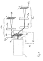
- the device according to the invention for remote sensing includes a front telescope 1 and a device 10 for separating two light beams, which has a double-column unit 11 and a deflection unit 12, and two spectrometers 13a, 13b, each with at least one optics 14a, 14b with collimators and mirrors , a disperser array 15a, 15b and matrix detectors 16a, 16b.
- the detectors 16a, 16b are sensitive in different wavelength ranges.
- the detector 16a can detect wavelengths of 400 to 900 nm and the detector 16b wavelengths of 900 to 2,500 nm. Any other division or partial overlap of the wavelength ranges is possible.
- the device 10 for separating the light bundles is shown in FIG Fig. 2a and Fig. 2b shown.
- the device is constructed in layers.
- the base material used is preferably silicon wafers (hereinafter Si wafers) or wafer material.
- the double-slit unit 11 is designed as a very thinly etched wafer, for example with a thickness of less than 0.3 mm with additional thinning to less than 5 ⁇ m.
- two rectangular gaps 11a, 11b are provided which have a length in the range of about 25 mm and a width in the range of about 24 ⁇ m.
- the gap between the columns is less than 480 ⁇ m with a gap width of 24 ⁇ m.
- the outline of the wafer plate which forms the double-column unit 11 is rectangular, but any other outline geometry that can be adapted specifically to the installation conditions can also be selected.
- a deflection unit 12 On the side facing away from the front telescope side of the double-column unit 11, a deflection unit 12 is provided, which is also formed as a layer.
- the deflection unit 12 can also be designed as a thinly etched Si wafer. For example, it has a thickness of less than 1 mm, about 0.9 mm.
- the deflection unit 12 has an oblique surface 12a acting as a mirror, which extends in its longitudinal extent at least over the length of the gaps 11a, 11b, and which forms the edge of the wafer in the region of the gaps 11a, 11b.
- the inclined surface 12a encloses an acute angle ⁇ with the plane in which the gaps 11a, 11b are arranged. The angle is chosen according to the geometric conditions.
- the surface is arranged so behind the columns, that, like out Fig. 2b It can be seen that a passing through the gap 11a light beam La occurs on the inclined surface 12a and is reflected at this at the angle ⁇ measured to the solder on the surface 12a.
- the length of the inclined surface 12a in the direction of the second gap 11b is dimensioned so that a passing through the second gap 11b light beam Lb just no longer impinges on the inclined surface 12a, but unhindered by the gap 11b and on the surface 12a of Deflection unit passes.
- a support structure 17 is arranged, which is also formed as a layer, preferably made of silicon material, and in the region adjacent to the column 11a, 11b has an aperture 17a.
- the thickness of the support structure 17 and the outline is adapted to the circumstances. The thickness is for example a few millimeters to allow a macroscopic version of the nip unit.
- a spacer layer 18 is arranged, which extends only as far as the aperture 17a, so that the light bundles can propagate behind the deflection unit.
- the structure consisting of support structure 17, double-column unit 11, deflection unit 12, spacer layer 18 and support structure 19 is as shown Fig.
- the carrier 20 is also formed of silicon.
- the front telescope facing side of the double-column unit 11 may be provided with a highly reflective coating, such as silver with silicon dioxide as a protective layer.
- the deflecting unit 12 facing side of the double-splitting unit 11 may be formed absorbent.
- an absorption layer of Ag-black or Si-black may be provided.
- the double-splitting unit 11 and the deflecting unit 12 are preferably formed by bonding such as bonding. Si-Si bonding, covalent bonding, etc., interconnected. For this they can have corresponding lithographic reference marks.
- the diaphragms and the spacer layer as well as the carrier are connected to the double-gap unit and the deflection unit via bonding.
- the gaps and mirror surfaces can be produced by the etching methods known in semiconductor technology.
- the mirror surfaces can be produced by classical optical polishing methods.
- the panels are manufactured using high-speed milling and cutting processes. The fact that all components are made of the same material, the entire structure has a high thermo-mechanical stability.
- the double-split unit 11 intersects, as in FIG Fig. 1 it can be seen on the image generated by the front telescope 1 in the plane of the double-column unit 11 two adjacent fields, which are represented by the light beams La and Lb.
- the direction of travel of the front telescope is transverse to the gap, so that the light beams La and Lb represent a local area with an extension transverse to the direction of travel.
- the light beam La passes through the gap 11a and is reflected by the deflection unit 12 at the inclined surface 12a at the angle ⁇ so that it exits through the opening 20a in the carrier and is deflected from there to the mirror system 14a.
- the image produced by the detector 16a is two-dimensional and includes in the line direction an image of the first local area represented by the beam 11a and in the column direction of its spectral decomposition.
- the passing through the gap 11 b light beam Lb which represents the second local area in the direction of movement of the front telescope, goes past the inclined surface 12 a undisturbed, passes through the aperture 19 a of the aperture 19 therethrough, where it then deflects a mirror system 14b and strikes the disperser assembly 15b, which spectrally decomposes the light beam Lb.
- the detector 16b which is the same as the detector 16a but is sensitive in a second wavelength range, a two-dimensional image of the second local area similar to the two-dimensional image of the first local area is generated only in the second spectral range.
- the structure of the device makes it possible to reduce the pitch of the gaps such that the local areas are very close to each other, so that the time offset in which they are swept is minimized. This increases the local co-registration of the generated images, as any instability in the orientation of the satellite has less influence.
- Fig. 3a and 3b show a second embodiment of the device for the separation of the light beams. Parts that are the same as those of the first embodiment according to Fig. 2a and Fig. 2b are given the same reference numerals and their description will not be repeated.
- the device 10 'for separating the light bundles comprises a modified deflection unit 12'.
- the modified deflection unit 12 ' has a first deflection unit 12 which is formed as in the first embodiment and which has an inclined surface 12a for deflecting the light beam La passing through the gap 11a and a second deflection unit 112 which passes through the gap 11b Light beam deflects Lb.
- the second deflection unit 112 is also formed of silicon material and is provided on the side facing away from the cleavage plane of the first deflection unit 12.
- the second deflector 112 has an inclined surface 112a which subtends an acute angle ⁇ with the plane in which the gaps are located. This is also chosen according to the geometric conditions.
- the inclined surface 112a of the second deflecting unit is so arranged, and the thickness of the second deflecting unit is selected so that the light beam Lb passing through the second gap 11b occurs at the angle ⁇ to the perpendicular on the inclined surface 112a and is reflected therefrom at this angle such that the reflected light beam Lb passes through the opening 20a in the carrier.
- the invention is not limited to a double-gap system, but more than two columns and a corresponding number of spectrometers may be provided which generate images in more than two wavelength ranges.
- the material for the layers any material can be used which can be processed with the usual methods in nanotechnology for the production of very small optomechanical structures.
- the compound of the layers can also be done by gluing.
- the invention is further not limited to the use in remote sensing.
- it may also serve to provide e.g. to allow in telecommunications in the optical signal transmission a spatial spectrally selected signal separation or general applications of imaging spectroscopy.
Landscapes
- Physics & Mathematics (AREA)
- Spectroscopy & Molecular Physics (AREA)
- General Physics & Mathematics (AREA)
- Optics & Photonics (AREA)
- Spectrometry And Color Measurement (AREA)
Applications Claiming Priority (1)
| Application Number | Priority Date | Filing Date | Title |
|---|---|---|---|
| DE200710036067 DE102007036067B4 (de) | 2007-08-01 | 2007-08-01 | Abbildendes Spektrometer, insbesondere für die optische Fernerkundung |
Publications (2)
| Publication Number | Publication Date |
|---|---|
| EP2026050A1 true EP2026050A1 (fr) | 2009-02-18 |
| EP2026050B1 EP2026050B1 (fr) | 2010-07-21 |
Family
ID=39876294
Family Applications (1)
| Application Number | Title | Priority Date | Filing Date |
|---|---|---|---|
| EP20080013866 Not-in-force EP2026050B1 (fr) | 2007-08-01 | 2008-08-01 | Spectromètre d'imagérie comprennant un dispositif de séparation d'au moins deux faisceaux lumineux représentant respectivement une zone spatiale |
Country Status (2)
| Country | Link |
|---|---|
| EP (1) | EP2026050B1 (fr) |
| DE (2) | DE102007036067B4 (fr) |
Cited By (1)
| Publication number | Priority date | Publication date | Assignee | Title |
|---|---|---|---|---|
| CN108078542A (zh) * | 2017-11-10 | 2018-05-29 | 上海康奥实业发展有限公司 | 高精度宽视野成像光谱仪装置 |
Families Citing this family (1)
| Publication number | Priority date | Publication date | Assignee | Title |
|---|---|---|---|---|
| DE102015112769B4 (de) * | 2015-08-04 | 2022-09-08 | Carl Zeiss Ag | Vorrichtung und Verfahren zur optischen Probenuntersuchung |
Citations (4)
| Publication number | Priority date | Publication date | Assignee | Title |
|---|---|---|---|---|
| DE899282C (de) * | 1952-02-23 | 1953-12-10 | Leitz Ernst Gmbh | Interferometer |
| EP0418705A2 (fr) * | 1989-09-22 | 1991-03-27 | Alcatel SEL Aktiengesellschaft | Laser à semi-conducteur interférométrique |
| DE3932886A1 (de) * | 1989-10-02 | 1991-04-11 | Guenter Knapp | Vorrichtung zur gleichzeitigen erfassung von zwei definierten wellenlaengenbereichen einer lichtstrahlung |
| WO1994007117A2 (fr) * | 1992-09-12 | 1994-03-31 | Geophysical And Environmental Research Corp. | Spectometre multibande aeroporte a formation d'images |
-
2007
- 2007-08-01 DE DE200710036067 patent/DE102007036067B4/de not_active Expired - Fee Related
-
2008
- 2008-08-01 EP EP20080013866 patent/EP2026050B1/fr not_active Not-in-force
- 2008-08-01 DE DE200850000978 patent/DE502008000978D1/de active Active
Patent Citations (4)
| Publication number | Priority date | Publication date | Assignee | Title |
|---|---|---|---|---|
| DE899282C (de) * | 1952-02-23 | 1953-12-10 | Leitz Ernst Gmbh | Interferometer |
| EP0418705A2 (fr) * | 1989-09-22 | 1991-03-27 | Alcatel SEL Aktiengesellschaft | Laser à semi-conducteur interférométrique |
| DE3932886A1 (de) * | 1989-10-02 | 1991-04-11 | Guenter Knapp | Vorrichtung zur gleichzeitigen erfassung von zwei definierten wellenlaengenbereichen einer lichtstrahlung |
| WO1994007117A2 (fr) * | 1992-09-12 | 1994-03-31 | Geophysical And Environmental Research Corp. | Spectometre multibande aeroporte a formation d'images |
Cited By (1)
| Publication number | Priority date | Publication date | Assignee | Title |
|---|---|---|---|---|
| CN108078542A (zh) * | 2017-11-10 | 2018-05-29 | 上海康奥实业发展有限公司 | 高精度宽视野成像光谱仪装置 |
Also Published As
| Publication number | Publication date |
|---|---|
| DE502008000978D1 (de) | 2010-09-02 |
| EP2026050B1 (fr) | 2010-07-21 |
| DE102007036067B4 (de) | 2010-09-16 |
| DE102007036067A1 (de) | 2009-02-19 |
Similar Documents
| Publication | Publication Date | Title |
|---|---|---|
| DE102010040768B4 (de) | Spektralzerlegungsvorrichtung und Herstellung derselben | |
| EP1336084B1 (fr) | Procede d'analyse de spectres d'echelles | |
| DE102009021440B4 (de) | Spektroskopiemodul und Verfahren zum Herstellen desselben | |
| DE102009021438A1 (de) | Spektroskopiemodul | |
| DE102009021436A1 (de) | Spektroskopiemodul | |
| DE19620807B4 (de) | Festkörperdetektor | |
| EP3260820B1 (fr) | Dispositif optique de mesure de position | |
| EP0529200B1 (fr) | Arrangement de capteurs d'image pour une caméra à capteurs multiples | |
| DE3918726C1 (fr) | ||
| EP2895843A1 (fr) | Appareil de mesure permettant de mesurer la luminescence | |
| DE20006642U1 (de) | Optische Vorrichtung | |
| EP1436647B1 (fr) | Procede de production d'une echelle graduee, echelle graduee produite selon ce procede et dispositif de mesure de position | |
| EP2980525A1 (fr) | Interféromètre à double passage | |
| DE60209419T2 (de) | Kollimator und Spektrophotometer | |
| EP1467185B1 (fr) | Ensemble lentille pour un codeur optique | |
| DE102009038028B4 (de) | Detektoranordnung mit erhöhter Empfindlichkeit durch Lichtablenkelemente mit einer ebenen Lichteintrittsfläche | |
| EP2026050B1 (fr) | Spectromètre d'imagérie comprennant un dispositif de séparation d'au moins deux faisceaux lumineux représentant respectivement une zone spatiale | |
| EP2521179B1 (fr) | Dispositif de détection du spectre de rayonnement électromagnétique à l'intérieur d'une zone de longueurs d'ondes prédéterminée | |
| DE102015108818A1 (de) | Anordnung zur Spektroskopie und Verfahren zur Herstellung der Anordnung | |
| DE102022110651B4 (de) | Kompaktes optisches Spektrometer | |
| DE102013112376B4 (de) | Spektrometersystem | |
| EP2738543A2 (fr) | Cellule de mesure interférométrique, spectromètre et procédé de mesure spectroscopique | |
| DE102011082469B4 (de) | Spektrometer mit wenigstens einem Zerstreuungselement | |
| WO2011058190A1 (fr) | Dispositif et procédé de localisation de sources de rayonnement optique modulées | |
| EP1967890A2 (fr) | Procédé de fabrication de composants de filtres multispectraux et agencement de filtre multispectral |
Legal Events
| Date | Code | Title | Description |
|---|---|---|---|
| PUAI | Public reference made under article 153(3) epc to a published international application that has entered the european phase |
Free format text: ORIGINAL CODE: 0009012 |
|
| AK | Designated contracting states |
Kind code of ref document: A1 Designated state(s): AT BE BG CH CY CZ DE DK EE ES FI FR GB GR HR HU IE IS IT LI LT LU LV MC MT NL NO PL PT RO SE SI SK TR |
|
| AX | Request for extension of the european patent |
Extension state: AL BA MK RS |
|
| 17P | Request for examination filed |
Effective date: 20090807 |
|
| 17Q | First examination report despatched |
Effective date: 20090903 |
|
| AKX | Designation fees paid |
Designated state(s): BE DE FR GB IT NL |
|
| GRAP | Despatch of communication of intention to grant a patent |
Free format text: ORIGINAL CODE: EPIDOSNIGR1 |
|
| RTI1 | Title (correction) |
Free format text: IMAGING SPECTROMETER COMPRISING A DEVICE FOR SEPARATING AT LEAST TWO LIGHT BEAMS, EACH REPRESENTING AN AREA |
|
| GRAS | Grant fee paid |
Free format text: ORIGINAL CODE: EPIDOSNIGR3 |
|
| GRAA | (expected) grant |
Free format text: ORIGINAL CODE: 0009210 |
|
| AK | Designated contracting states |
Kind code of ref document: B1 Designated state(s): BE DE FR GB IT NL |
|
| REG | Reference to a national code |
Ref country code: GB Ref legal event code: FG4D Free format text: NOT ENGLISH |
|
| REF | Corresponds to: |
Ref document number: 502008000978 Country of ref document: DE Date of ref document: 20100902 Kind code of ref document: P |
|
| REG | Reference to a national code |
Ref country code: NL Ref legal event code: T3 |
|
| PLBE | No opposition filed within time limit |
Free format text: ORIGINAL CODE: 0009261 |
|
| STAA | Information on the status of an ep patent application or granted ep patent |
Free format text: STATUS: NO OPPOSITION FILED WITHIN TIME LIMIT |
|
| 26N | No opposition filed |
Effective date: 20110426 |
|
| REG | Reference to a national code |
Ref country code: DE Ref legal event code: R097 Ref document number: 502008000978 Country of ref document: DE Effective date: 20110426 |
|
| REG | Reference to a national code |
Ref country code: FR Ref legal event code: PLFP Year of fee payment: 9 |
|
| REG | Reference to a national code |
Ref country code: FR Ref legal event code: PLFP Year of fee payment: 10 |
|
| REG | Reference to a national code |
Ref country code: FR Ref legal event code: PLFP Year of fee payment: 11 |
|
| PGFP | Annual fee paid to national office [announced via postgrant information from national office to epo] |
Ref country code: NL Payment date: 20200820 Year of fee payment: 13 |
|
| PGFP | Annual fee paid to national office [announced via postgrant information from national office to epo] |
Ref country code: GB Payment date: 20200825 Year of fee payment: 13 Ref country code: FR Payment date: 20200820 Year of fee payment: 13 |
|
| PGFP | Annual fee paid to national office [announced via postgrant information from national office to epo] |
Ref country code: IT Payment date: 20200831 Year of fee payment: 13 Ref country code: BE Payment date: 20200820 Year of fee payment: 13 |
|
| REG | Reference to a national code |
Ref country code: NL Ref legal event code: MM Effective date: 20210901 |
|
| REG | Reference to a national code |
Ref country code: BE Ref legal event code: MM Effective date: 20210831 |
|
| GBPC | Gb: european patent ceased through non-payment of renewal fee |
Effective date: 20210801 |
|
| PG25 | Lapsed in a contracting state [announced via postgrant information from national office to epo] |
Ref country code: NL Free format text: LAPSE BECAUSE OF NON-PAYMENT OF DUE FEES Effective date: 20210901 |
|
| PG25 | Lapsed in a contracting state [announced via postgrant information from national office to epo] |
Ref country code: IT Free format text: LAPSE BECAUSE OF NON-PAYMENT OF DUE FEES Effective date: 20210801 Ref country code: GB Free format text: LAPSE BECAUSE OF NON-PAYMENT OF DUE FEES Effective date: 20210801 Ref country code: FR Free format text: LAPSE BECAUSE OF NON-PAYMENT OF DUE FEES Effective date: 20210831 Ref country code: BE Free format text: LAPSE BECAUSE OF NON-PAYMENT OF DUE FEES Effective date: 20210831 |
|
| PGFP | Annual fee paid to national office [announced via postgrant information from national office to epo] |
Ref country code: DE Payment date: 20240827 Year of fee payment: 17 |
|
| REG | Reference to a national code |
Ref country code: DE Ref legal event code: R119 Ref document number: 502008000978 Country of ref document: DE |