EP2045373A2 - Reacteur epitaxial utilise dans la production de plaquettes a grande echelle - Google Patents
Reacteur epitaxial utilise dans la production de plaquettes a grande echelle Download PDFInfo
- Publication number
- EP2045373A2 EP2045373A2 EP06794026A EP06794026A EP2045373A2 EP 2045373 A2 EP2045373 A2 EP 2045373A2 EP 06794026 A EP06794026 A EP 06794026A EP 06794026 A EP06794026 A EP 06794026A EP 2045373 A2 EP2045373 A2 EP 2045373A2
- Authority
- EP
- European Patent Office
- Prior art keywords
- chamber
- susceptors
- gas
- wafers
- mass production
- Prior art date
- Legal status (The legal status is an assumption and is not a legal conclusion. Google has not performed a legal analysis and makes no representation as to the accuracy of the status listed.)
- Granted
Links
Images


Classifications
-
- C—CHEMISTRY; METALLURGY
- C30—CRYSTAL GROWTH
- C30B—SINGLE-CRYSTAL GROWTH; UNIDIRECTIONAL SOLIDIFICATION OF EUTECTIC MATERIAL OR UNIDIRECTIONAL DEMIXING OF EUTECTOID MATERIAL; REFINING BY ZONE-MELTING OF MATERIAL; PRODUCTION OF A HOMOGENEOUS POLYCRYSTALLINE MATERIAL WITH DEFINED STRUCTURE; SINGLE CRYSTALS OR HOMOGENEOUS POLYCRYSTALLINE MATERIAL WITH DEFINED STRUCTURE; AFTER-TREATMENT OF SINGLE CRYSTALS OR A HOMOGENEOUS POLYCRYSTALLINE MATERIAL WITH DEFINED STRUCTURE; APPARATUS THEREFOR
- C30B25/00—Single-crystal growth by chemical reaction of reactive gases, e.g. chemical vapour-deposition growth
- C30B25/02—Epitaxial-layer growth
-
- C—CHEMISTRY; METALLURGY
- C30—CRYSTAL GROWTH
- C30B—SINGLE-CRYSTAL GROWTH; UNIDIRECTIONAL SOLIDIFICATION OF EUTECTIC MATERIAL OR UNIDIRECTIONAL DEMIXING OF EUTECTOID MATERIAL; REFINING BY ZONE-MELTING OF MATERIAL; PRODUCTION OF A HOMOGENEOUS POLYCRYSTALLINE MATERIAL WITH DEFINED STRUCTURE; SINGLE CRYSTALS OR HOMOGENEOUS POLYCRYSTALLINE MATERIAL WITH DEFINED STRUCTURE; AFTER-TREATMENT OF SINGLE CRYSTALS OR A HOMOGENEOUS POLYCRYSTALLINE MATERIAL WITH DEFINED STRUCTURE; APPARATUS THEREFOR
- C30B25/00—Single-crystal growth by chemical reaction of reactive gases, e.g. chemical vapour-deposition growth
- C30B25/02—Epitaxial-layer growth
- C30B25/12—Substrate holders or susceptors
-
- C—CHEMISTRY; METALLURGY
- C23—COATING METALLIC MATERIAL; COATING MATERIAL WITH METALLIC MATERIAL; CHEMICAL SURFACE TREATMENT; DIFFUSION TREATMENT OF METALLIC MATERIAL; COATING BY VACUUM EVAPORATION, BY SPUTTERING, BY ION IMPLANTATION OR BY CHEMICAL VAPOUR DEPOSITION, IN GENERAL; INHIBITING CORROSION OF METALLIC MATERIAL OR INCRUSTATION IN GENERAL
- C23C—COATING METALLIC MATERIAL; COATING MATERIAL WITH METALLIC MATERIAL; SURFACE TREATMENT OF METALLIC MATERIAL BY DIFFUSION INTO THE SURFACE, BY CHEMICAL CONVERSION OR SUBSTITUTION; COATING BY VACUUM EVAPORATION, BY SPUTTERING, BY ION IMPLANTATION OR BY CHEMICAL VAPOUR DEPOSITION, IN GENERAL
- C23C16/00—Chemical coating by decomposition of gaseous compounds, without leaving reaction products of surface material in the coating, i.e. chemical vapour deposition [CVD] processes
- C23C16/44—Chemical coating by decomposition of gaseous compounds, without leaving reaction products of surface material in the coating, i.e. chemical vapour deposition [CVD] processes characterised by the method of coating
- C23C16/455—Chemical coating by decomposition of gaseous compounds, without leaving reaction products of surface material in the coating, i.e. chemical vapour deposition [CVD] processes characterised by the method of coating characterised by the method used for introducing gases into reaction chamber or for modifying gas flows in reaction chamber
- C23C16/45502—Flow conditions in reaction chamber
- C23C16/45504—Laminar flow
-
- C—CHEMISTRY; METALLURGY
- C23—COATING METALLIC MATERIAL; COATING MATERIAL WITH METALLIC MATERIAL; CHEMICAL SURFACE TREATMENT; DIFFUSION TREATMENT OF METALLIC MATERIAL; COATING BY VACUUM EVAPORATION, BY SPUTTERING, BY ION IMPLANTATION OR BY CHEMICAL VAPOUR DEPOSITION, IN GENERAL; INHIBITING CORROSION OF METALLIC MATERIAL OR INCRUSTATION IN GENERAL
- C23C—COATING METALLIC MATERIAL; COATING MATERIAL WITH METALLIC MATERIAL; SURFACE TREATMENT OF METALLIC MATERIAL BY DIFFUSION INTO THE SURFACE, BY CHEMICAL CONVERSION OR SUBSTITUTION; COATING BY VACUUM EVAPORATION, BY SPUTTERING, BY ION IMPLANTATION OR BY CHEMICAL VAPOUR DEPOSITION, IN GENERAL
- C23C16/00—Chemical coating by decomposition of gaseous compounds, without leaving reaction products of surface material in the coating, i.e. chemical vapour deposition [CVD] processes
- C23C16/44—Chemical coating by decomposition of gaseous compounds, without leaving reaction products of surface material in the coating, i.e. chemical vapour deposition [CVD] processes characterised by the method of coating
- C23C16/455—Chemical coating by decomposition of gaseous compounds, without leaving reaction products of surface material in the coating, i.e. chemical vapour deposition [CVD] processes characterised by the method of coating characterised by the method used for introducing gases into reaction chamber or for modifying gas flows in reaction chamber
- C23C16/45593—Recirculation of reactive gases
-
- C—CHEMISTRY; METALLURGY
- C30—CRYSTAL GROWTH
- C30B—SINGLE-CRYSTAL GROWTH; UNIDIRECTIONAL SOLIDIFICATION OF EUTECTIC MATERIAL OR UNIDIRECTIONAL DEMIXING OF EUTECTOID MATERIAL; REFINING BY ZONE-MELTING OF MATERIAL; PRODUCTION OF A HOMOGENEOUS POLYCRYSTALLINE MATERIAL WITH DEFINED STRUCTURE; SINGLE CRYSTALS OR HOMOGENEOUS POLYCRYSTALLINE MATERIAL WITH DEFINED STRUCTURE; AFTER-TREATMENT OF SINGLE CRYSTALS OR A HOMOGENEOUS POLYCRYSTALLINE MATERIAL WITH DEFINED STRUCTURE; APPARATUS THEREFOR
- C30B25/00—Single-crystal growth by chemical reaction of reactive gases, e.g. chemical vapour-deposition growth
- C30B25/02—Epitaxial-layer growth
- C30B25/08—Reaction chambers; Selection of materials therefor
-
- C—CHEMISTRY; METALLURGY
- C30—CRYSTAL GROWTH
- C30B—SINGLE-CRYSTAL GROWTH; UNIDIRECTIONAL SOLIDIFICATION OF EUTECTIC MATERIAL OR UNIDIRECTIONAL DEMIXING OF EUTECTOID MATERIAL; REFINING BY ZONE-MELTING OF MATERIAL; PRODUCTION OF A HOMOGENEOUS POLYCRYSTALLINE MATERIAL WITH DEFINED STRUCTURE; SINGLE CRYSTALS OR HOMOGENEOUS POLYCRYSTALLINE MATERIAL WITH DEFINED STRUCTURE; AFTER-TREATMENT OF SINGLE CRYSTALS OR A HOMOGENEOUS POLYCRYSTALLINE MATERIAL WITH DEFINED STRUCTURE; APPARATUS THEREFOR
- C30B25/00—Single-crystal growth by chemical reaction of reactive gases, e.g. chemical vapour-deposition growth
- C30B25/02—Epitaxial-layer growth
- C30B25/14—Feed and outlet means for the gases; Modifying the flow of the reactive gases
-
- C—CHEMISTRY; METALLURGY
- C30—CRYSTAL GROWTH
- C30B—SINGLE-CRYSTAL GROWTH; UNIDIRECTIONAL SOLIDIFICATION OF EUTECTIC MATERIAL OR UNIDIRECTIONAL DEMIXING OF EUTECTOID MATERIAL; REFINING BY ZONE-MELTING OF MATERIAL; PRODUCTION OF A HOMOGENEOUS POLYCRYSTALLINE MATERIAL WITH DEFINED STRUCTURE; SINGLE CRYSTALS OR HOMOGENEOUS POLYCRYSTALLINE MATERIAL WITH DEFINED STRUCTURE; AFTER-TREATMENT OF SINGLE CRYSTALS OR A HOMOGENEOUS POLYCRYSTALLINE MATERIAL WITH DEFINED STRUCTURE; APPARATUS THEREFOR
- C30B35/00—Apparatus not otherwise provided for, specially adapted for the growth, production or after-treatment of single crystals or of a homogeneous polycrystalline material with defined structure
-
- H—ELECTRICITY
- H10—SEMICONDUCTOR DEVICES; ELECTRIC SOLID-STATE DEVICES NOT OTHERWISE PROVIDED FOR
- H10F—INORGANIC SEMICONDUCTOR DEVICES SENSITIVE TO INFRARED RADIATION, LIGHT, ELECTROMAGNETIC RADIATION OF SHORTER WAVELENGTH OR CORPUSCULAR RADIATION
- H10F71/00—Manufacture or treatment of devices covered by this subclass
-
- H—ELECTRICITY
- H10—SEMICONDUCTOR DEVICES; ELECTRIC SOLID-STATE DEVICES NOT OTHERWISE PROVIDED FOR
- H10P—GENERIC PROCESSES OR APPARATUS FOR THE MANUFACTURE OR TREATMENT OF DEVICES COVERED BY CLASS H10
- H10P72/00—Handling or holding of wafers, substrates or devices during manufacture or treatment thereof
- H10P72/70—Handling or holding of wafers, substrates or devices during manufacture or treatment thereof for supporting or gripping
- H10P72/76—Handling or holding of wafers, substrates or devices during manufacture or treatment thereof for supporting or gripping using mechanical means, e.g. clamps or pinches
- H10P72/7604—Handling or holding of wafers, substrates or devices during manufacture or treatment thereof for supporting or gripping using mechanical means, e.g. clamps or pinches the wafers being placed on a susceptor, stage or support
- H10P72/7616—Handling or holding of wafers, substrates or devices during manufacture or treatment thereof for supporting or gripping using mechanical means, e.g. clamps or pinches the wafers being placed on a susceptor, stage or support characterised by a coating, a hardness or a material
-
- H—ELECTRICITY
- H10—SEMICONDUCTOR DEVICES; ELECTRIC SOLID-STATE DEVICES NOT OTHERWISE PROVIDED FOR
- H10P—GENERIC PROCESSES OR APPARATUS FOR THE MANUFACTURE OR TREATMENT OF DEVICES COVERED BY CLASS H10
- H10P72/00—Handling or holding of wafers, substrates or devices during manufacture or treatment thereof
- H10P72/70—Handling or holding of wafers, substrates or devices during manufacture or treatment thereof for supporting or gripping
- H10P72/76—Handling or holding of wafers, substrates or devices during manufacture or treatment thereof for supporting or gripping using mechanical means, e.g. clamps or pinches
- H10P72/7604—Handling or holding of wafers, substrates or devices during manufacture or treatment thereof for supporting or gripping using mechanical means, e.g. clamps or pinches the wafers being placed on a susceptor, stage or support
- H10P72/7621—Handling or holding of wafers, substrates or devices during manufacture or treatment thereof for supporting or gripping using mechanical means, e.g. clamps or pinches the wafers being placed on a susceptor, stage or support characterised by supporting two or more semiconductor substrates
-
- H—ELECTRICITY
- H10—SEMICONDUCTOR DEVICES; ELECTRIC SOLID-STATE DEVICES NOT OTHERWISE PROVIDED FOR
- H10P—GENERIC PROCESSES OR APPARATUS FOR THE MANUFACTURE OR TREATMENT OF DEVICES COVERED BY CLASS H10
- H10P72/00—Handling or holding of wafers, substrates or devices during manufacture or treatment thereof
- H10P72/70—Handling or holding of wafers, substrates or devices during manufacture or treatment thereof for supporting or gripping
- H10P72/76—Handling or holding of wafers, substrates or devices during manufacture or treatment thereof for supporting or gripping using mechanical means, e.g. clamps or pinches
- H10P72/7604—Handling or holding of wafers, substrates or devices during manufacture or treatment thereof for supporting or gripping using mechanical means, e.g. clamps or pinches the wafers being placed on a susceptor, stage or support
- H10P72/7624—Handling or holding of wafers, substrates or devices during manufacture or treatment thereof for supporting or gripping using mechanical means, e.g. clamps or pinches the wafers being placed on a susceptor, stage or support characterised by the mechanical construction of the susceptor, stage or support
Definitions
- the present invention is framed in the sector of chemical vapor deposition growth processes, more concretely epitaxial growth processes, within microelectronic and photovoltaic industry.
- Silicon epitaxial growth by chemical vapor deposition is a widely known and applied process in microelectronics. It consists on the formation of a crystalline material thin film (around 20-50 ⁇ m) on a thick crystalline substrate (around 300 ⁇ m) in such a way that the atoms in the epitaxial layer reproduce the crystallographic structure of the substrate. This is achieved by flowing a silicon containing gas (a chlorosilane, for instance), called source gas, diluted in a so called carrier gas, over the substrate where growth is wanted. This substrate is heated up to the temperature at which source gas pyrolisis and consequent atomic silicon deposition take place.
- a silicon containing gas a chlorosilane, for instance
- carrier gas diluted in a so called carrier gas
- the advantage in using an epitaxial reactor is that it allows fabricating the solar cell in a thin silicon epitaxial layer of high purity, grown on a silicon substrate of much lower quality.
- a high-throughput epitaxial reactor able to produce epitaxied silicon semiconductor layers in a big scale, for instance 250 to 1000 wafers per process, for the photovoltaic industry.
- the Fraunhofer ISE Institute in Freiburg, Germany has developed a continuous epitaxial reactor, in which substrates continuously pass through the epitaxial chamber carried on bands.
- the solution adopted by the present invention consists of an epitaxial reactor where substrates are very densely stacked, separated around 4 cm from one another, in a way that many substrates can be processed at the same time in a big chamber.
- induction or infrared lamp heating is substituted by Joule effect, which allows the desired stacking density for the invention's configuration, and is also very efficient in energy use.
- the present invention incorporates recycling of usually more than 90 % of the used gas, providing big savings in gas costs, especially in carrier gas. All of this can contribute to cost reduction in solar cell production.
- the microelectronic industry can also benefit from all or at least some of the aspects of the present invention.
- the present invention is a reactor for chemical vapor deposition, mainly intended for the epitaxial deposition of silicon for electronic or photovoltaic devices.
- silane as well as chlorosilanes can be used as silicon source gases which are carried to the deposition surface in a carrier gas flow (hydrogen, nitrogen, argon, etc).
- a carrier gas flow hydrogen, nitrogen, argon, etc.
- the gas mixture enters the sealed chamber directly into the pre-chamber, flows through it upwards, then flows between the susceptors and exits the chamber by a gas outlet pipe, helped by the chamber's upper wall tilting towards that outlet. See rest of document for the explanation of each single part mentioned above.
- the substrates or conductive wafers where the epitaxial layer is to be deposited are placed on densely stacked graphite (or other conductive material) susceptors.
- This allows a large number of samples to be processed per batch, between 250 and 1000, so that the throughput is very much increased with respect to the commercial reactors used for those purposes.
- the time employed in heating and cooling becomes very small in a per substrate basis thus significantly reducing the amortization costs.
- Another characteristic of the proposed design, also leading to reduced deposition costs, is the efficient heating system employed.
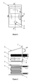
- the reactor chamber is shown in Figures 1 and 2 .
- the chamber connection panel (1) is fixed and allocates all sensitive parts of the reactor, such as the electrical (7) and gas (5 and 6) connections, and other feedthroughs needed for instrumentation and control (8).
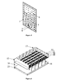
- the susceptors are vertically placed, electrically interconnected by parts of the same conductive material (4). For their mechanical support, besides being attached to the panel at their ends, they can rest on columns of an isolating material.
- the gas is first introduced into a pre-chamber (3), which is either welded or simply attached to the panel (1), where it is mixed and evenly distributed in the spaces between susceptors.
- the rest of the chamber walls form a housing (2) that moves to open and close the chamber.
- a high throughput process is obtained by the present invention, which is a reactor where susceptors are densely stacked, separated some 4 cm from one another, allowing a high number of semiconductor wafers (which are the epitaxy substrates) per run, from 250 to 1000.
- these susceptors (4) are rectangular plates of conductive material placed vertically in front of each other (parallel). They are series connected with additional parts (9) of the same conductive material, which allows the whole conductive block to conduct electricity, acting as a resistance which is easily heated to the adequate deposition temperature by Joule effect when an electrical current flows.
- This heating method is not conventionally used in commercial epitaxial reactors, which use either induction heating by induction coils, or infrared heating by lamps. Joule effect is a much more efficient heating method. Energy efficiency is also assisted by the fact that hot susceptors radiate to the neighbouring ones and by the high reflectance of the walls, so that most of the radiation is kept inside the reaction chamber.
- Susceptors have a slightly trapezoidal section, i.e., they are slightly tilted, with a broader base and a thinner upper side.
- the substrates lie on both sides of the susceptors, held by specially designed holders, so that they do not fall down.
- interducts (10) are thus the real "reaction chambers", i.e., the space to be considered for all calculations regarding deposition.
- the reactor of the present invention is constituted by a sealed chamber externally water cooled, and internally covered by reflecting material, that is assembled to a gas recirculation system and that contains: a pre-chamber, a variable number of stacked, vertical, parallel to one another susceptors, heated by Joule effect; semiconductor wafers placed on the susceptors and held to them by holders of the susceptors' same material; a fixed connection panel, where electrical and thermocouple connections, and gas inlet and outlet are found, which is attached to the pre-chamber by welding, screwing or similar; and a housing that slides on rails, which opens and closes the chamber by uncoupling from or coupling to the connection panel.
- the reactor is composed by a chamber, made of stainless steel or other metallic material, which is internally covered by a reflective material, thus reflecting back most (around 85 %) of the radiation produced by the hot susceptors, and externally cooled by water.
- the reflective layer avoids excessive heating of the chamber walls, which brings about further advantages: energetic losses are reduced, therefore a lower water flow is needed for refrigeration, inexpensive materials can be used for joints, etc, since they do not have to stand high temperatures, there is no need for an otherwise expensive quartz chamber, etc.
- the quartz chamber can be provided if wanted for contamination reduction of the semiconductive wafers, but is not necessary for other purposes.
- the radiation between hot neighbouring susceptors is, on the other hand, the main factor that helps keep susceptor temperature very homogeneous along its surface. This is a key factor for a homogeneous deposition and crystal growth, and therefore good epitaxy quality. In fact, it is this same temperature homogeneity requirement the one that sets a limit to the stacking density of the susceptors, for, if these are placed very close to each other, homogeneity is lost.
- the susceptors also feature cylindrical, vertical holes to accommodate thermocouples for temperature measurement and control purposes.
- the present invention includes a simple system for electrical feedthroughs, which connects the cold outer wall with the hot susceptors, with a temperature difference of around 1000 °C. It can be seen in Figure 4 .
- the idea is to provide a prolongation (12) of the susceptor (4) where electrical connections are needed. This prolongation (12) is enclosed in an extra stainless-steel chamber (7) protruding from the connection panel, as explained later.
- connection panel schematically represented in Figure 5 .
- the panel is the only fixed part of the chamber, being the rest of it an open box or housing consisting of the walls. This box can move, and slides on bars to open and close the chamber.
- the connection panel itself is fixed and can allocate gas inlet (5) and outlet (6), electrical feedthroughs (7), and thermocouple or other purpose feedthroughs (8), and it also mechanically supports the pre-chamber (see Figures 6 , 7 and 10 ), which is welded to it, and the susceptors (see Figures 3 and 10 ), which are connected to the panel via the electrical feedthroughs.
- a single, non-movable block consisting of panel, susceptors and pre-chamber is formed and the reactor's most sensitive parts are fixed, they do not move. The risks associated to the movement of delicate parts when opening and closing or manipulating are thus avoided.
- Gas inlet (5) is situated, together with thermocouple and other feedthroughs (8), in the lower part of the connection panel. Chamber extensions for the electrical feedthroughs (7) are situated just above them.
- the upper part of the connection panel has a chimney-like extension (6) which facilitates the gas exiting the chamber. Additionally, the upper side of the movable reactor walls is tilted towards the panel, to avoid gas flow disruption and further helping gas outlet (see Figure 1 ).
- connection panel is provided with a vacuum joint system and appropriate closure mechanisms. It can allocate two concentric joints. Having two joints instead of one is an additional safety and precaution measure to avoid gas leaks through the connection panel.
- the inner one seals the chamber when this is closed, and the outer one acts as a further safety sealing. Between both joints vacuum is made, and pressure strictly controlled by a pressure control system coupled to the space between joints. An increase in pressure would mean that a leak is produced in the inner or the outer seal. If this occurs, the control system must stop the process immediately. This vacuum should be enough to ensure that the vacuum chamber is properly closed, but additional clasps are provided to mechanically attach the connection panel to the rest of the chamber when the reactor is closed.
- pre-chamber A further crucial part of the novel reactor design is the so called pre-chamber, depicted in Figures 6 and 7 . It is a stainless steel chamber placed inside the reactor chamber and below the susceptors. It has three main functions:
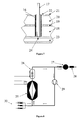
- the hot gas exits the reactor (25) to enter directly into a heat exchanger (26), where it is cooled down to near room temperature.
- a heat exchanger 26
- the flow splits, and part of the gas is vented out by means of an extraction pump (27) and flows through a neutralizer (28), whereas most of it is recirculated back into the reaction chamber (25) by means of a gas blower (29).
- the species in the recirculated stream can react so that the gas composition changes, and this has to be taken into account when mixing the recirculated stream with the fresh stream (30) before entering the reaction chamber (25) again.
- the hydrogen chloride concentration increases as a side product of the deposition: there is a maximum that should not be exceeded, otherwise etching of the silicon surface starts being more important than the growth itself.
- a second version of the recirculation implies in-situ formation of the source gas, and is represented in Figure 9 .
- the starting material for the deposition is not a silicon-containing gas, but solid silicon, which can be ultrapure silicon, or for instance metallurgical grade silicon (mg-Si), or upgraded metallurgical grade silicon (umg-Si), both of them cheaper.
- this silicon reacts to form a mixture of chlorosilanes, whose composition depends on the conditions used.
- the desired species in the appropriate concentration is thus obtained.
- This interesting concept implies theoretical deposition efficiencies of 100 % and theoretical carrier gas consumption of zero.
- This gas recirculation system includes in situ formation of source gas by HCl etching of solid silicon, and includes a heat exchanger at the deposition chamber exit, a solid silicon etching chamber, another heat exchanger at the exit of this etching chamber, and initial gas feed.
Landscapes
- Chemical & Material Sciences (AREA)
- Metallurgy (AREA)
- Engineering & Computer Science (AREA)
- Materials Engineering (AREA)
- Organic Chemistry (AREA)
- General Chemical & Material Sciences (AREA)
- Chemical Kinetics & Catalysis (AREA)
- Crystallography & Structural Chemistry (AREA)
- Mechanical Engineering (AREA)
- Physics & Mathematics (AREA)
- Fluid Mechanics (AREA)
- Chemical Vapour Deposition (AREA)
- Nitrogen And Oxygen Or Sulfur-Condensed Heterocyclic Ring Systems (AREA)
- Heterocyclic Carbon Compounds Containing A Hetero Ring Having Oxygen Or Sulfur (AREA)
Applications Claiming Priority (2)
| Application Number | Priority Date | Filing Date | Title |
|---|---|---|---|
| ES200501461A ES2268974B2 (es) | 2005-06-16 | 2005-06-16 | Reactor epitaxial para la produccion de obleas a gran escala. |
| PCT/ES2006/000351 WO2006134194A2 (fr) | 2005-06-16 | 2006-06-15 | Reacteur epitaxial utilise dans la production de plaquettes a grande echelle |
Publications (2)
| Publication Number | Publication Date |
|---|---|
| EP2045373A2 true EP2045373A2 (fr) | 2009-04-08 |
| EP2045373B1 EP2045373B1 (fr) | 2010-10-27 |
Family
ID=37532658
Family Applications (1)
| Application Number | Title | Priority Date | Filing Date |
|---|---|---|---|
| EP06794026A Not-in-force EP2045373B1 (fr) | 2005-06-16 | 2006-06-15 | Reacteur epitaxial utilise dans la production de plaquettes a grande echelle |
Country Status (6)
| Country | Link |
|---|---|
| US (1) | US8435349B2 (fr) |
| EP (1) | EP2045373B1 (fr) |
| AT (1) | ATE486159T1 (fr) |
| DE (1) | DE602006017904D1 (fr) |
| ES (1) | ES2268974B2 (fr) |
| WO (1) | WO2006134194A2 (fr) |
Families Citing this family (3)
| Publication number | Priority date | Publication date | Assignee | Title |
|---|---|---|---|---|
| US9870937B2 (en) | 2010-06-09 | 2018-01-16 | Ob Realty, Llc | High productivity deposition reactor comprising a gas flow chamber having a tapered gas flow space |
| EP2659504A4 (fr) * | 2010-12-31 | 2014-05-07 | Solexel Inc | Systèmes et procédés de dépôt |
| US10047457B2 (en) * | 2013-09-16 | 2018-08-14 | Applied Materials, Inc. | EPI pre-heat ring |
Family Cites Families (6)
| Publication number | Priority date | Publication date | Assignee | Title |
|---|---|---|---|---|
| US3460510A (en) * | 1966-05-12 | 1969-08-12 | Dow Corning | Large volume semiconductor coating reactor |
| US4694779A (en) * | 1984-10-19 | 1987-09-22 | Tetron, Inc. | Reactor apparatus for semiconductor wafer processing |
| ES2011105A6 (es) * | 1988-07-28 | 1989-12-16 | Fundacion General De La Univer | Reactor epitaxial de susceptores concentrados. |
| ES2011115A6 (es) | 1988-09-27 | 1989-12-16 | Perez Perez Manuel | Maquina peladora de almendras. |
| JPH0598449A (ja) * | 1991-10-02 | 1993-04-20 | Ibiden Co Ltd | プラズマcvd装置のサセプタに使用されるウエハ保持ピン |
| DE19655219C2 (de) * | 1996-04-24 | 2003-11-06 | Steag Micro Tech Gmbh | Vorrichtung zum Behandeln von Substraten in einem Fluid-Behälter |
-
2005
- 2005-06-16 ES ES200501461A patent/ES2268974B2/es not_active Expired - Fee Related
-
2006
- 2006-06-15 AT AT06794026T patent/ATE486159T1/de not_active IP Right Cessation
- 2006-06-15 US US11/921,950 patent/US8435349B2/en not_active Expired - Fee Related
- 2006-06-15 WO PCT/ES2006/000351 patent/WO2006134194A2/fr not_active Ceased
- 2006-06-15 EP EP06794026A patent/EP2045373B1/fr not_active Not-in-force
- 2006-06-15 DE DE602006017904T patent/DE602006017904D1/de active Active
Non-Patent Citations (1)
| Title |
|---|
| See references of WO2006134194A2 * |
Also Published As
| Publication number | Publication date |
|---|---|
| WO2006134194A3 (fr) | 2007-04-12 |
| US8435349B2 (en) | 2013-05-07 |
| ES2268974A1 (es) | 2007-03-16 |
| ATE486159T1 (de) | 2010-11-15 |
| DE602006017904D1 (de) | 2010-12-09 |
| WO2006134194A2 (fr) | 2006-12-21 |
| US20090217877A1 (en) | 2009-09-03 |
| ES2268974B2 (es) | 2007-12-01 |
| EP2045373B1 (fr) | 2010-10-27 |
| WO2006134194B1 (fr) | 2007-05-24 |
Similar Documents
| Publication | Publication Date | Title |
|---|---|---|
| US8673081B2 (en) | High throughput multi-wafer epitaxial reactor | |
| Faller et al. | High-temperature CVD for crystalline-silicon thin-film solar cells | |
| CN102421934B (zh) | 高产量多晶片外延反应器 | |
| US6284312B1 (en) | Method and apparatus for chemical vapor deposition of polysilicon | |
| TW379359B (en) | Dual vertical thermal processing furnace | |
| KR101853274B1 (ko) | 기판 상에 재료들을 증착하기 위한 방법들 및 장치 | |
| KR880000472B1 (ko) | 화학 증착 장치 및 방법 | |
| EP1257684B1 (fr) | Procede et appareil de depot chimique en phase vapeur de silicium polycristallin | |
| US6365225B1 (en) | Cold wall reactor and method for chemical vapor deposition of bulk polysilicon | |
| CN116411265B (zh) | 一种化学气相沉积装置及其方法 | |
| US20100047447A1 (en) | Multiple substrate item holder and reactor | |
| JPH02150040A (ja) | 気相成長装置 | |
| CN107022789A (zh) | 在外延反应器中的硅衬底上外延沉积硅晶片的方法 | |
| US20160298263A1 (en) | Process gas preheating systems and methods for double-sided multi-substrate batch processing | |
| EP2045373B1 (fr) | Reacteur epitaxial utilise dans la production de plaquettes a grande echelle | |
| US4547404A (en) | Chemical vapor deposition process | |
| US20110000425A1 (en) | Method of manufacturing semiconductor device, method of manufacturing substrate, and substrate processing apparatus | |
| US7381926B2 (en) | Removable heater | |
| CN116926506A (zh) | 一种纵长形反应腔体及其化学气相沉积装置 | |
| US4279669A (en) | Method for epitaxial deposition | |
| JPH07273101A (ja) | 枚葉式熱処理装置 | |
| JP2658213B2 (ja) | 気相エピタキシャル成長方法 | |
| Sarma et al. | Continuous growth of polycrystalline silicon films by chemical vapor deposition | |
| CN102652107A (zh) | 多晶硅的制造方法及多晶硅制造用反应炉 | |
| JP2013193931A (ja) | 多結晶シリコンロッドの製造方法 |
Legal Events
| Date | Code | Title | Description |
|---|---|---|---|
| PUAI | Public reference made under article 153(3) epc to a published international application that has entered the european phase |
Free format text: ORIGINAL CODE: 0009012 |
|
| 17P | Request for examination filed |
Effective date: 20071221 |
|
| AK | Designated contracting states |
Kind code of ref document: A2 Designated state(s): AT BE BG CH CY CZ DE DK EE ES FI FR GB GR HU IE IS IT LI LT LU LV MC NL PL PT RO SE SI SK TR |
|
| RIC1 | Information provided on ipc code assigned before grant |
Ipc: C30B 25/02 20060101ALI20090407BHEP Ipc: C30B 25/12 20060101AFI20071217BHEP Ipc: C30B 25/08 20060101ALI20090407BHEP Ipc: C30B 25/14 20060101ALI20090407BHEP |
|
| 17Q | First examination report despatched |
Effective date: 20080116 |
|
| GRAP | Despatch of communication of intention to grant a patent |
Free format text: ORIGINAL CODE: EPIDOSNIGR1 |
|
| GRAS | Grant fee paid |
Free format text: ORIGINAL CODE: EPIDOSNIGR3 |
|
| GRAA | (expected) grant |
Free format text: ORIGINAL CODE: 0009210 |
|
| AK | Designated contracting states |
Kind code of ref document: B1 Designated state(s): AT BE BG CH CY CZ DE DK EE ES FI FR GB GR HU IE IS IT LI LT LU LV MC NL PL PT RO SE SI SK TR |
|
| REG | Reference to a national code |
Ref country code: GB Ref legal event code: FG4D |
|
| REG | Reference to a national code |
Ref country code: CH Ref legal event code: EP |
|
| REG | Reference to a national code |
Ref country code: IE Ref legal event code: FG4D |
|
| REF | Corresponds to: |
Ref document number: 602006017904 Country of ref document: DE Date of ref document: 20101209 Kind code of ref document: P |
|
| REG | Reference to a national code |
Ref country code: NL Ref legal event code: T3 |
|
| LTIE | Lt: invalidation of european patent or patent extension |
Effective date: 20101027 |
|
| PG25 | Lapsed in a contracting state [announced via postgrant information from national office to epo] |
Ref country code: LT Free format text: LAPSE BECAUSE OF FAILURE TO SUBMIT A TRANSLATION OF THE DESCRIPTION OR TO PAY THE FEE WITHIN THE PRESCRIBED TIME-LIMIT Effective date: 20101027 |
|
| PG25 | Lapsed in a contracting state [announced via postgrant information from national office to epo] |
Ref country code: SI Free format text: LAPSE BECAUSE OF FAILURE TO SUBMIT A TRANSLATION OF THE DESCRIPTION OR TO PAY THE FEE WITHIN THE PRESCRIBED TIME-LIMIT Effective date: 20101027 Ref country code: BG Free format text: LAPSE BECAUSE OF FAILURE TO SUBMIT A TRANSLATION OF THE DESCRIPTION OR TO PAY THE FEE WITHIN THE PRESCRIBED TIME-LIMIT Effective date: 20110127 Ref country code: SE Free format text: LAPSE BECAUSE OF FAILURE TO SUBMIT A TRANSLATION OF THE DESCRIPTION OR TO PAY THE FEE WITHIN THE PRESCRIBED TIME-LIMIT Effective date: 20101027 Ref country code: FI Free format text: LAPSE BECAUSE OF FAILURE TO SUBMIT A TRANSLATION OF THE DESCRIPTION OR TO PAY THE FEE WITHIN THE PRESCRIBED TIME-LIMIT Effective date: 20101027 Ref country code: AT Free format text: LAPSE BECAUSE OF FAILURE TO SUBMIT A TRANSLATION OF THE DESCRIPTION OR TO PAY THE FEE WITHIN THE PRESCRIBED TIME-LIMIT Effective date: 20101027 Ref country code: IS Free format text: LAPSE BECAUSE OF FAILURE TO SUBMIT A TRANSLATION OF THE DESCRIPTION OR TO PAY THE FEE WITHIN THE PRESCRIBED TIME-LIMIT Effective date: 20110227 Ref country code: PT Free format text: LAPSE BECAUSE OF FAILURE TO SUBMIT A TRANSLATION OF THE DESCRIPTION OR TO PAY THE FEE WITHIN THE PRESCRIBED TIME-LIMIT Effective date: 20110228 Ref country code: LV Free format text: LAPSE BECAUSE OF FAILURE TO SUBMIT A TRANSLATION OF THE DESCRIPTION OR TO PAY THE FEE WITHIN THE PRESCRIBED TIME-LIMIT Effective date: 20101027 |
|
| PG25 | Lapsed in a contracting state [announced via postgrant information from national office to epo] |
Ref country code: BE Free format text: LAPSE BECAUSE OF FAILURE TO SUBMIT A TRANSLATION OF THE DESCRIPTION OR TO PAY THE FEE WITHIN THE PRESCRIBED TIME-LIMIT Effective date: 20101027 Ref country code: GR Free format text: LAPSE BECAUSE OF FAILURE TO SUBMIT A TRANSLATION OF THE DESCRIPTION OR TO PAY THE FEE WITHIN THE PRESCRIBED TIME-LIMIT Effective date: 20110128 |
|
| PG25 | Lapsed in a contracting state [announced via postgrant information from national office to epo] |
Ref country code: EE Free format text: LAPSE BECAUSE OF FAILURE TO SUBMIT A TRANSLATION OF THE DESCRIPTION OR TO PAY THE FEE WITHIN THE PRESCRIBED TIME-LIMIT Effective date: 20101027 Ref country code: ES Free format text: LAPSE BECAUSE OF FAILURE TO SUBMIT A TRANSLATION OF THE DESCRIPTION OR TO PAY THE FEE WITHIN THE PRESCRIBED TIME-LIMIT Effective date: 20110207 Ref country code: CZ Free format text: LAPSE BECAUSE OF FAILURE TO SUBMIT A TRANSLATION OF THE DESCRIPTION OR TO PAY THE FEE WITHIN THE PRESCRIBED TIME-LIMIT Effective date: 20101027 |
|
| PG25 | Lapsed in a contracting state [announced via postgrant information from national office to epo] |
Ref country code: RO Free format text: LAPSE BECAUSE OF FAILURE TO SUBMIT A TRANSLATION OF THE DESCRIPTION OR TO PAY THE FEE WITHIN THE PRESCRIBED TIME-LIMIT Effective date: 20101027 Ref country code: DK Free format text: LAPSE BECAUSE OF FAILURE TO SUBMIT A TRANSLATION OF THE DESCRIPTION OR TO PAY THE FEE WITHIN THE PRESCRIBED TIME-LIMIT Effective date: 20101027 Ref country code: PL Free format text: LAPSE BECAUSE OF FAILURE TO SUBMIT A TRANSLATION OF THE DESCRIPTION OR TO PAY THE FEE WITHIN THE PRESCRIBED TIME-LIMIT Effective date: 20101027 Ref country code: SK Free format text: LAPSE BECAUSE OF FAILURE TO SUBMIT A TRANSLATION OF THE DESCRIPTION OR TO PAY THE FEE WITHIN THE PRESCRIBED TIME-LIMIT Effective date: 20101027 |
|
| PLBE | No opposition filed within time limit |
Free format text: ORIGINAL CODE: 0009261 |
|
| STAA | Information on the status of an ep patent application or granted ep patent |
Free format text: STATUS: NO OPPOSITION FILED WITHIN TIME LIMIT |
|
| 26N | No opposition filed |
Effective date: 20110728 |
|
| REG | Reference to a national code |
Ref country code: DE Ref legal event code: R097 Ref document number: 602006017904 Country of ref document: DE Effective date: 20110728 |
|
| PG25 | Lapsed in a contracting state [announced via postgrant information from national office to epo] |
Ref country code: IT Free format text: LAPSE BECAUSE OF FAILURE TO SUBMIT A TRANSLATION OF THE DESCRIPTION OR TO PAY THE FEE WITHIN THE PRESCRIBED TIME-LIMIT Effective date: 20101027 |
|
| REG | Reference to a national code |
Ref country code: CH Ref legal event code: PL |
|
| REG | Reference to a national code |
Ref country code: IE Ref legal event code: MM4A |
|
| PG25 | Lapsed in a contracting state [announced via postgrant information from national office to epo] |
Ref country code: IE Free format text: LAPSE BECAUSE OF NON-PAYMENT OF DUE FEES Effective date: 20110615 Ref country code: CH Free format text: LAPSE BECAUSE OF NON-PAYMENT OF DUE FEES Effective date: 20110630 Ref country code: LI Free format text: LAPSE BECAUSE OF NON-PAYMENT OF DUE FEES Effective date: 20110630 |
|
| PG25 | Lapsed in a contracting state [announced via postgrant information from national office to epo] |
Ref country code: MC Free format text: LAPSE BECAUSE OF NON-PAYMENT OF DUE FEES Effective date: 20110630 |
|
| PG25 | Lapsed in a contracting state [announced via postgrant information from national office to epo] |
Ref country code: CY Free format text: LAPSE BECAUSE OF FAILURE TO SUBMIT A TRANSLATION OF THE DESCRIPTION OR TO PAY THE FEE WITHIN THE PRESCRIBED TIME-LIMIT Effective date: 20101027 Ref country code: LU Free format text: LAPSE BECAUSE OF NON-PAYMENT OF DUE FEES Effective date: 20110615 |
|
| PG25 | Lapsed in a contracting state [announced via postgrant information from national office to epo] |
Ref country code: TR Free format text: LAPSE BECAUSE OF FAILURE TO SUBMIT A TRANSLATION OF THE DESCRIPTION OR TO PAY THE FEE WITHIN THE PRESCRIBED TIME-LIMIT Effective date: 20101027 |
|
| PG25 | Lapsed in a contracting state [announced via postgrant information from national office to epo] |
Ref country code: HU Free format text: LAPSE BECAUSE OF FAILURE TO SUBMIT A TRANSLATION OF THE DESCRIPTION OR TO PAY THE FEE WITHIN THE PRESCRIBED TIME-LIMIT Effective date: 20101027 |
|
| REG | Reference to a national code |
Ref country code: FR Ref legal event code: PLFP Year of fee payment: 10 |
|
| PGFP | Annual fee paid to national office [announced via postgrant information from national office to epo] |
Ref country code: GB Payment date: 20150618 Year of fee payment: 10 |
|
| PGFP | Annual fee paid to national office [announced via postgrant information from national office to epo] |
Ref country code: NL Payment date: 20150623 Year of fee payment: 10 |
|
| PGFP | Annual fee paid to national office [announced via postgrant information from national office to epo] |
Ref country code: DE Payment date: 20150831 Year of fee payment: 10 |
|
| PGFP | Annual fee paid to national office [announced via postgrant information from national office to epo] |
Ref country code: FR Payment date: 20150630 Year of fee payment: 10 |
|
| REG | Reference to a national code |
Ref country code: DE Ref legal event code: R119 Ref document number: 602006017904 Country of ref document: DE |
|
| REG | Reference to a national code |
Ref country code: NL Ref legal event code: MM Effective date: 20160701 |
|
| GBPC | Gb: european patent ceased through non-payment of renewal fee |
Effective date: 20160615 |
|
| REG | Reference to a national code |
Ref country code: FR Ref legal event code: ST Effective date: 20170228 |
|
| PG25 | Lapsed in a contracting state [announced via postgrant information from national office to epo] |
Ref country code: FR Free format text: LAPSE BECAUSE OF NON-PAYMENT OF DUE FEES Effective date: 20160630 Ref country code: DE Free format text: LAPSE BECAUSE OF NON-PAYMENT OF DUE FEES Effective date: 20170103 |
|
| PG25 | Lapsed in a contracting state [announced via postgrant information from national office to epo] |
Ref country code: GB Free format text: LAPSE BECAUSE OF NON-PAYMENT OF DUE FEES Effective date: 20160615 Ref country code: NL Free format text: LAPSE BECAUSE OF NON-PAYMENT OF DUE FEES Effective date: 20160701 |