EP2045641A2 - Dispositif d'éclairage - Google Patents
Dispositif d'éclairage Download PDFInfo
- Publication number
- EP2045641A2 EP2045641A2 EP08163492A EP08163492A EP2045641A2 EP 2045641 A2 EP2045641 A2 EP 2045641A2 EP 08163492 A EP08163492 A EP 08163492A EP 08163492 A EP08163492 A EP 08163492A EP 2045641 A2 EP2045641 A2 EP 2045641A2
- Authority
- EP
- European Patent Office
- Prior art keywords
- light
- laser
- lighting device
- optical element
- spectrally
- Prior art date
- Legal status (The legal status is an assumption and is not a legal conclusion. Google has not performed a legal analysis and makes no representation as to the accuracy of the status listed.)
- Ceased
Links
Images


Classifications
-
- G—PHYSICS
- G02—OPTICS
- G02B—OPTICAL ELEMENTS, SYSTEMS OR APPARATUS
- G02B6/00—Light guides; Structural details of arrangements comprising light guides and other optical elements, e.g. couplings
- G02B6/02—Optical fibres with cladding with or without a coating
- G02B6/02295—Microstructured optical fibre
- G02B6/02314—Plurality of longitudinal structures extending along optical fibre axis, e.g. holes
- G02B6/02342—Plurality of longitudinal structures extending along optical fibre axis, e.g. holes characterised by cladding features, i.e. light confining region
- G02B6/02376—Longitudinal variation along fibre axis direction, e.g. tapered holes
-
- G—PHYSICS
- G01—MEASURING; TESTING
- G01J—MEASUREMENT OF INTENSITY, VELOCITY, SPECTRAL CONTENT, POLARISATION, PHASE OR PULSE CHARACTERISTICS OF INFRARED, VISIBLE OR ULTRAVIOLET LIGHT; COLORIMETRY; RADIATION PYROMETRY
- G01J3/00—Spectrometry; Spectrophotometry; Monochromators; Measuring colours
- G01J3/02—Details
- G01J3/0205—Optical elements not provided otherwise, e.g. optical manifolds, diffusers, windows
- G01J3/0218—Optical elements not provided otherwise, e.g. optical manifolds, diffusers, windows using optical fibers
-
- G—PHYSICS
- G01—MEASURING; TESTING
- G01J—MEASUREMENT OF INTENSITY, VELOCITY, SPECTRAL CONTENT, POLARISATION, PHASE OR PULSE CHARACTERISTICS OF INFRARED, VISIBLE OR ULTRAVIOLET LIGHT; COLORIMETRY; RADIATION PYROMETRY
- G01J3/00—Spectrometry; Spectrophotometry; Monochromators; Measuring colours
- G01J3/02—Details
- G01J3/10—Arrangements of light sources specially adapted for spectrometry or colorimetry
-
- G—PHYSICS
- G01—MEASURING; TESTING
- G01J—MEASUREMENT OF INTENSITY, VELOCITY, SPECTRAL CONTENT, POLARISATION, PHASE OR PULSE CHARACTERISTICS OF INFRARED, VISIBLE OR ULTRAVIOLET LIGHT; COLORIMETRY; RADIATION PYROMETRY
- G01J3/00—Spectrometry; Spectrophotometry; Monochromators; Measuring colours
- G01J3/12—Generating the spectrum; Monochromators
- G01J3/1256—Generating the spectrum; Monochromators using acousto-optic tunable filter
-
- G—PHYSICS
- G02—OPTICS
- G02B—OPTICAL ELEMENTS, SYSTEMS OR APPARATUS
- G02B21/00—Microscopes
- G02B21/0004—Microscopes specially adapted for specific applications
- G02B21/002—Scanning microscopes
-
- G—PHYSICS
- G02—OPTICS
- G02B—OPTICAL ELEMENTS, SYSTEMS OR APPARATUS
- G02B21/00—Microscopes
- G02B21/0004—Microscopes specially adapted for specific applications
- G02B21/002—Scanning microscopes
- G02B21/0024—Confocal scanning microscopes (CSOMs) or confocal "macroscopes"; Accessories which are not restricted to use with CSOMs, e.g. sample holders
- G02B21/0032—Optical details of illumination, e.g. light-sources, pinholes, beam splitters, slits, fibers
-
- G—PHYSICS
- G02—OPTICS
- G02B—OPTICAL ELEMENTS, SYSTEMS OR APPARATUS
- G02B21/00—Microscopes
- G02B21/0004—Microscopes specially adapted for specific applications
- G02B21/002—Scanning microscopes
- G02B21/0024—Confocal scanning microscopes (CSOMs) or confocal "macroscopes"; Accessories which are not restricted to use with CSOMs, e.g. sample holders
- G02B21/0052—Optical details of the image generation
- G02B21/0056—Optical details of the image generation based on optical coherence, e.g. phase-contrast arrangements, interference arrangements
-
- G—PHYSICS
- G02—OPTICS
- G02B—OPTICAL ELEMENTS, SYSTEMS OR APPARATUS
- G02B21/00—Microscopes
- G02B21/0004—Microscopes specially adapted for specific applications
- G02B21/002—Scanning microscopes
- G02B21/0024—Confocal scanning microscopes (CSOMs) or confocal "macroscopes"; Accessories which are not restricted to use with CSOMs, e.g. sample holders
- G02B21/0052—Optical details of the image generation
- G02B21/0064—Optical details of the image generation multi-spectral or wavelength-selective arrangements, e.g. wavelength fan-out, chromatic profiling
-
- G—PHYSICS
- G02—OPTICS
- G02B—OPTICAL ELEMENTS, SYSTEMS OR APPARATUS
- G02B21/00—Microscopes
- G02B21/0004—Microscopes specially adapted for specific applications
- G02B21/002—Scanning microscopes
- G02B21/0024—Confocal scanning microscopes (CSOMs) or confocal "macroscopes"; Accessories which are not restricted to use with CSOMs, e.g. sample holders
- G02B21/0052—Optical details of the image generation
- G02B21/0076—Optical details of the image generation arrangements using fluorescence or luminescence
-
- G—PHYSICS
- G02—OPTICS
- G02B—OPTICAL ELEMENTS, SYSTEMS OR APPARATUS
- G02B21/00—Microscopes
- G02B21/0004—Microscopes specially adapted for specific applications
- G02B21/002—Scanning microscopes
- G02B21/0024—Confocal scanning microscopes (CSOMs) or confocal "macroscopes"; Accessories which are not restricted to use with CSOMs, e.g. sample holders
- G02B21/008—Details of detection or image processing, including general computer control
-
- G—PHYSICS
- G02—OPTICS
- G02B—OPTICAL ELEMENTS, SYSTEMS OR APPARATUS
- G02B21/00—Microscopes
- G02B21/06—Means for illuminating specimens
-
- G—PHYSICS
- G02—OPTICS
- G02B—OPTICAL ELEMENTS, SYSTEMS OR APPARATUS
- G02B6/00—Light guides; Structural details of arrangements comprising light guides and other optical elements, e.g. couplings
- G02B6/24—Coupling light guides
- G02B6/255—Splicing of light guides, e.g. by fusion or bonding
- G02B6/2552—Splicing of light guides, e.g. by fusion or bonding reshaping or reforming of light guides for coupling using thermal heating, e.g. tapering, forming of a lens on light guide ends
-
- G—PHYSICS
- G02—OPTICS
- G02F—OPTICAL DEVICES OR ARRANGEMENTS FOR THE CONTROL OF LIGHT BY MODIFICATION OF THE OPTICAL PROPERTIES OF THE MEDIA OF THE ELEMENTS INVOLVED THEREIN; NON-LINEAR OPTICS; FREQUENCY-CHANGING OF LIGHT; OPTICAL LOGIC ELEMENTS; OPTICAL ANALOGUE/DIGITAL CONVERTERS
- G02F1/00—Devices or arrangements for the control of the intensity, colour, phase, polarisation or direction of light arriving from an independent light source, e.g. switching, gating or modulating; Non-linear optics
- G02F1/35—Non-linear optics
- G02F1/353—Frequency conversion, i.e. wherein a light beam is generated with frequency components different from those of the incident light beams
-
- B—PERFORMING OPERATIONS; TRANSPORTING
- B82—NANOTECHNOLOGY
- B82Y—SPECIFIC USES OR APPLICATIONS OF NANOSTRUCTURES; MEASUREMENT OR ANALYSIS OF NANOSTRUCTURES; MANUFACTURE OR TREATMENT OF NANOSTRUCTURES
- B82Y20/00—Nanooptics, e.g. quantum optics or photonic crystals
-
- G—PHYSICS
- G02—OPTICS
- G02B—OPTICAL ELEMENTS, SYSTEMS OR APPARATUS
- G02B6/00—Light guides; Structural details of arrangements comprising light guides and other optical elements, e.g. couplings
- G02B6/02—Optical fibres with cladding with or without a coating
- G02B6/02295—Microstructured optical fibre
- G02B6/02314—Plurality of longitudinal structures extending along optical fibre axis, e.g. holes
- G02B6/02342—Plurality of longitudinal structures extending along optical fibre axis, e.g. holes characterised by cladding features, i.e. light confining region
- G02B6/02366—Single ring of structures, e.g. "air clad"
-
- G—PHYSICS
- G02—OPTICS
- G02B—OPTICAL ELEMENTS, SYSTEMS OR APPARATUS
- G02B6/00—Light guides; Structural details of arrangements comprising light guides and other optical elements, e.g. couplings
- G02B6/02—Optical fibres with cladding with or without a coating
- G02B6/02295—Microstructured optical fibre
- G02B6/02314—Plurality of longitudinal structures extending along optical fibre axis, e.g. holes
- G02B6/02342—Plurality of longitudinal structures extending along optical fibre axis, e.g. holes characterised by cladding features, i.e. light confining region
- G02B6/02371—Cross section of longitudinal structures is non-circular
-
- G—PHYSICS
- G02—OPTICS
- G02F—OPTICAL DEVICES OR ARRANGEMENTS FOR THE CONTROL OF LIGHT BY MODIFICATION OF THE OPTICAL PROPERTIES OF THE MEDIA OF THE ELEMENTS INVOLVED THEREIN; NON-LINEAR OPTICS; FREQUENCY-CHANGING OF LIGHT; OPTICAL LOGIC ELEMENTS; OPTICAL ANALOGUE/DIGITAL CONVERTERS
- G02F1/00—Devices or arrangements for the control of the intensity, colour, phase, polarisation or direction of light arriving from an independent light source, e.g. switching, gating or modulating; Non-linear optics
- G02F1/35—Non-linear optics
- G02F1/3528—Non-linear optics for producing a supercontinuum
-
- G—PHYSICS
- G02—OPTICS
- G02F—OPTICAL DEVICES OR ARRANGEMENTS FOR THE CONTROL OF LIGHT BY MODIFICATION OF THE OPTICAL PROPERTIES OF THE MEDIA OF THE ELEMENTS INVOLVED THEREIN; NON-LINEAR OPTICS; FREQUENCY-CHANGING OF LIGHT; OPTICAL LOGIC ELEMENTS; OPTICAL ANALOGUE/DIGITAL CONVERTERS
- G02F2202/00—Materials and properties
- G02F2202/32—Photonic crystals
-
- H—ELECTRICITY
- H01—ELECTRIC ELEMENTS
- H01S—DEVICES USING THE PROCESS OF LIGHT AMPLIFICATION BY STIMULATED EMISSION OF RADIATION [LASER] TO AMPLIFY OR GENERATE LIGHT; DEVICES USING STIMULATED EMISSION OF ELECTROMAGNETIC RADIATION IN WAVE RANGES OTHER THAN OPTICAL
- H01S3/00—Lasers, i.e. devices using stimulated emission of electromagnetic radiation in the infrared, visible or ultraviolet wave range
- H01S3/005—Optical devices external to the laser cavity, specially adapted for lasers, e.g. for homogenisation of the beam or for manipulating laser pulses, e.g. pulse shaping
-
- H—ELECTRICITY
- H01—ELECTRIC ELEMENTS
- H01S—DEVICES USING THE PROCESS OF LIGHT AMPLIFICATION BY STIMULATED EMISSION OF RADIATION [LASER] TO AMPLIFY OR GENERATE LIGHT; DEVICES USING STIMULATED EMISSION OF ELECTROMAGNETIC RADIATION IN WAVE RANGES OTHER THAN OPTICAL
- H01S3/00—Lasers, i.e. devices using stimulated emission of electromagnetic radiation in the infrared, visible or ultraviolet wave range
- H01S3/14—Lasers, i.e. devices using stimulated emission of electromagnetic radiation in the infrared, visible or ultraviolet wave range characterised by the material used as the active medium
- H01S3/16—Solid materials
- H01S3/1601—Solid materials characterised by an active (lasing) ion
- H01S3/162—Solid materials characterised by an active (lasing) ion transition metal
- H01S3/1625—Solid materials characterised by an active (lasing) ion transition metal titanium
-
- H—ELECTRICITY
- H01—ELECTRIC ELEMENTS
- H01S—DEVICES USING THE PROCESS OF LIGHT AMPLIFICATION BY STIMULATED EMISSION OF RADIATION [LASER] TO AMPLIFY OR GENERATE LIGHT; DEVICES USING STIMULATED EMISSION OF ELECTROMAGNETIC RADIATION IN WAVE RANGES OTHER THAN OPTICAL
- H01S3/00—Lasers, i.e. devices using stimulated emission of electromagnetic radiation in the infrared, visible or ultraviolet wave range
- H01S3/14—Lasers, i.e. devices using stimulated emission of electromagnetic radiation in the infrared, visible or ultraviolet wave range characterised by the material used as the active medium
- H01S3/16—Solid materials
- H01S3/163—Solid materials characterised by a crystal matrix
- H01S3/1631—Solid materials characterised by a crystal matrix aluminate
- H01S3/1636—Al2O3 (Sapphire)
Definitions
- the invention relates to a lighting device with a laser emitting a light beam, which is directed to a microstructured optical element, which spectrally widens the light of the laser.
- the system includes an ultrashort pulse laser for generating ultrashort optical pulses of a fixed wavelength and at least one wavelength conversion channel.
- the patent US 6,097,870 discloses an arrangement for generating a broadband spectrum in the visible and infrared spectral range.
- the arrangement is based on a microstructured fiber into which the light of a pump laser is coupled.
- the pump light is broadened in the microstructured fiber by non-linear effects.
- a microstructured fiber so-called photonic band gap material or "photonic crystal fibers”, “holey fibers” or “microstructured fibers” are also used.
- Embodiments are also known as so-called "hollow fiber”.
- Arc lamps are known as broadband light sources and are used in many areas. Exemplary here is the U.S. Patent 3,720,822 "XENON PHOTOGRAPHY LIGHT", which reveals a xenon arc lamp for illumination in photography.
- Multicolor Fluorescence Confocal Microscope System is known to be a single laser array laser emitting system. At present, mostly mixed gas lasers, in particular ArKr lasers, are used for this purpose.
- ArKr lasers are used for this purpose.
- a sample for example, prepared with fluorescent dyes, biological tissues or sections are examined.
- the illumination light reflected by the sample is often detected. Solid state lasers and dye lasers, as well as fiber lasers and optical parametric oscillators (OPO), which are preceded by a pump laser, are frequently used.
- the known from the prior art lighting devices have several disadvantages.
- the known broadband illumination devices usually have a low luminance in comparison to laser-based illumination devices, while these provide the user with only discrete wavelength lines whose spectral position and width, if at all, can only be adjusted to a small extent. Due to this limitation of the working spectrum, the known lighting devices can not be used flexibly.
- the invention has for its object to provide a lighting device that avoids or solves the disadvantages and problems.
- the objective object is achieved by an arrangement including the features of the characterizing part of claim 1.
- the invention has the advantage that it is universally applicable, easy to handle and flexible and also offers light from a wide wavelength range.
- the illumination device has a housing with a light exit opening, from which the spectrally broadened light emerges. This has the advantage that in particular the optical components are protected from external influences and in particular from contamination.
- microstructured optical element is followed by an optical system which forms the spectrally broadened light into a beam.
- This optic is preferably located inside the housing immediately before or in the light exit opening.
- a, preferably mounted on the housing, warning lamp is provided which indicates the user the activity of the illumination device.
- the laser is a short-pulse laser, for example a mode-locked or mode-locked solid-state laser which emits light pulses having a duration of 100 fs to 10 ps.
- the illumination device which includes a device for varying the power of the spectrally broadened light. It is particularly advantageous in this case to design the illumination device in such a way that the power of the spectrally broadened light can be variably or completely faded out with respect to at least one selectable wavelength or at least one selectable wavelength range.
- acousto-optic or electro-optical elements such as acousto-optic tunable filters (AOTF)
- AOTF acousto-optic tunable filters
- dielectric filters or color filters can be used, which are preferably arranged in cascade. A special flexibility is achieved by the filters are mounted in revolvers or in sliding frames, which allow easy insertion into the beam path of the spectrally broadened light.
- a prism or a grid can be used.
- a Fabry-Perot filter is provided in a further embodiment variant.
- LCD filters can also be used.
- the housing controls for adjusting the light output and the spectral composition of the spectrally broadened light.
- these parameters are set on an external control panel or on a PC and the adjustment data are transmitted in the form of electrical signals to the illumination device or to the device for varying the power of the spectrally broadened light.
- the setting via sliders which are shown on a display and are operated, for example, with a computer mouse.
- the illumination device includes a focusing optics that the light beam of the laser focused on the microstructured optical element.
- focusing optics as Variooptik, for example as zoom optics.
- a device which allows an analysis of the wavelength-broadened light, in particular with regard to the spectral composition and the light output.
- the analysis device is arranged such that part of the spectrally broadened light is split off, for example with the aid of a beam splitter, and supplied to the analysis device.
- the analyzer is preferably a spectrometer. It contains, for example, a prism or a grating for spatial spectral splitting and a CCD element or a multi-channel photomultiplier as a detector.
- the analysis system includes a multiband detector. Semiconductor spectrometers are also usable.
- the detectors are designed such that an electrical signal proportional to the light power is generated, which can be evaluated by an electronic system or a computer.
- the embodiment which includes an indication of the power of the spectrally broadened light and / or the spectral composition of the spectrally broadened light.
- the display is preferably mounted directly on the housing or the control panel.
- the monitor of a PC is used to display the power or the spectral composition.
- the microstructured optical element is constructed in a preferred embodiment of the scanning microscope from a plurality of micro-optical structural elements having at least two different optical densities.
- the optical element includes a first region and a second region, wherein the first region has a homogeneous structure and in the second region a microscopic structure of microoptical structural elements is formed. It is also advantageous if the first Area encloses the second area.
- the micro-optical structural elements are preferably cannulas, webs, honeycombs, tubes or cavities.
- the microstructured optical element consists of juxtaposed glass or plastic material and cavities.
- the microstructured optical element consists of photonic band-gap material and is designed as an optical fiber, wherein preferably an optical diode is provided between the laser and the optical fiber, the back reflection of the light beam of the laser, which originates from the ends of the optical fiber, suppressed.
- a particularly preferred and easy-to-implement embodiment includes as a microstructured optical element, a conventional optical fiber with a fiber diameter of about 9 microns, which has a taper at least along a portion.
- Optical fibers of this type are known as so-called "tapered fibers".
- the optical fiber is a total of 1 m long and has a taper to a length of 30 mm to 90 mm.
- the diameter of the optical fiber is in a preferred embodiment in the region of the taper about 2 microns.
- the fiber core diameter is accordingly in the nanometer range.
- the illumination device is particularly suitable for illuminating a microscopic sample, in particular in a scanning microscope or confocal scanning microscope.
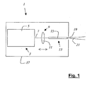
- Fig. 1 shows a lighting device 1, which includes a laser 3, which is designed as a diode laser pumped, mode-locked Ti: sapphire laser 5 and which emits a pulsed light beam 7, which is shown in dashed lines.
- the duration of the light pulses is about 100 fs at a repetition rate of about 80 MHz.
- the light beam 7 is focused with the focusing optics 9, which is designed as a zoom lens 11 and slidably disposed along the propagation direction of the light beam, to a microstructured optical element 13, which consists of a crystal 15 of photonic band Gap material. In the microstructured optical element, the light of the laser is spectrally broadened.
- All components are located in a housing 17 with a light exit opening 19 through which the spectrally broadened light 21, as a divergent beam, leaves the housing.
- the spectrum of the spectrally broadened light 21 ranges from about 300 nm to 1600 nm, wherein the light output over the entire spectrum is largely constant.
- Fig. 2 shows an embodiment analogous to that in Fig. 1 illustrated embodiment.
- an optical system 23 which forms the spectrally broadened light 21 in such a way to a spectrally broadened light beam 25, that this runs in a collimated manner.
- the optics 23 is designed as a vario-look.
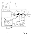
- Fig. 3 shows an embodiment analogous to that in Fig. 1 illustrated embodiment.
- the microstructured optical element 13 consists of photonic band gap material and is designed as an optical fiber 27.
- the spectrally broadened light 21 emerging from the optical fiber 27 becomes a collimated, spectrally broadened light beam 25 with the aid of the optical system 29 shaped.
- a partial light beam 33 of the spectrally broadened light beam 25 is split off and directed to an analysis device 35.
- the photodiode array 41 generates electric signals proportional to the power of the light of the respective spectral range, which are supplied to a processing unit 43. There, the signals are processed and forwarded to a display 44.
- a display 44 This consists of an LCD display 45 mounted on the housing, in which the composition of the spectrally broadened light 21 is displayed in the form of a graph 47 within a coordinate system with two axes 49, 51. On the axis 49, the wavelength is plotted and on the axis 51, the power of light.
- the lighting device shown includes a control panel 53 with a control knob 55, which serves to adjust the output power of the Ti: sapphire laser 5. By adjusting the power of the light beam 7, it is possible to vary the power of the spectrally broadened light 21.
- Fig. 4 shows a lighting device 1, which in the basic structure of in Fig. 3 corresponds to the illumination device shown.
- the microstructured optical element 13 consists of an optical fiber 57 having a taper 59.
- a computer 63 is used as the control console.
- the representation is analogous to that in Fig. 3 shown coordinate representation.
- the computer 63 controls in accordance with the user specification a device for varying the power 67 of the spectrally broadened light 21. This is designed as AOTF 69 (acousto optical tunable filter).
- AOTF 69 acousto optical tunable filter
- the user makes adjustments using the computer mouse 65.
- a slider 71 is shown, which serves to adjust the overall performance of the spectrally altered light 21.
- a dashed graph 73 is generated, which is deformable according to the movement of the computer mouse 65.
- the power varying device 67 is driven by the computer 63 to provide the spectral composition preselected by the dashed graph 73.
- Fig. 5 shows a lighting device as in Fig. 1 which additionally includes a display 75 for the power of the spectrally spread light 21, which is implemented as a pure number representation display.
- a partial beam 33 is split off from the spectrally broadened light 21 and directed to a photomultiplier 77, which generates an electrical signal proportional to the power of the impinging partial beam 33. This is processed in the processing unit 79 and transmitted to the display 75.
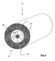
- Fig. 6 shows an embodiment of the microstructured optical element 13.
- This consists of photonic band Gap material having a particular honeycomb microstructure 81.
- the honeycomb structure shown is particularly suitable for the generation of broadband light.
- the diameter of the glass inner cannula 83 is about 1.9 microns.
- the inner cannula 83 is surrounded by glass webs 85.
- the glass webs 85 form honeycomb-shaped cavities 87.
- These micro-optical structural elements together form a second region 89, which is surrounded by a first region 91, the glass jacket is executed.
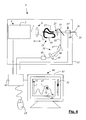
- Fig. 7 1 schematically shows a confocal scanning microscope 93.
- the light beam 25 coming from the illumination device 1 is reflected by a beam splitter 95 to the scanning module 97, which contains a gimbal-mounted scanning mirror 99 which guides the light beam 25 through the microscope optics 101 over or through the specimen 103 ,
- the light beam 25 is guided over the object surface in the case of non-transparent preparations 103.
- the light beam 25 can also be guided through the preparation 103. This means that from different focal planes of the preparation 103 successively scanned by the light beam 25.
- the Subsequent composition then gives a three-dimensional image of the preparation.
- the coming of the illumination device 1 light beam 25 is shown in the figure as a solid line.
- the light 105 emanating from the preparation 103 passes through the microscope optics 101 and via the scan module 97 to the beam splitter 95, passes through the latter and strikes detector 107, which is embodied as a photomultiplier.
- detector 107 which is embodied as a photomultiplier.
- the light 105 emanating from the preparation 103 is shown as a dashed line.
- electrical proportional to the performance of the outgoing of the preparation 103 light 105 detection signals are generated and further processed.
- the illumination pinhole 109 and the detection pinhole 111 usually provided in a confocal scanning microscope are shown schematically for the sake of completeness. By contrast, some optical elements for guiding and shaping the light beams have been omitted because of better clarity. These are well known to a person skilled in the art.
- Fig. 8 schematically shows an embodiment of the microstructured optical element 13.
- the microstructured optical element 13 of a conventional optical fiber 113 having an outer diameter of 125 microns and a Fasererkem 115 having a diameter of 6 microns.
- the outer diameter of the optical fiber 113 is reduced to 1.8 ⁇ m.
- the diameter of the fiber core 115 is only fractions of microns.
Landscapes
- Physics & Mathematics (AREA)
- General Physics & Mathematics (AREA)
- Spectroscopy & Molecular Physics (AREA)
- Optics & Photonics (AREA)
- Chemical & Material Sciences (AREA)
- Analytical Chemistry (AREA)
- Nonlinear Science (AREA)
- Engineering & Computer Science (AREA)
- General Engineering & Computer Science (AREA)
- Computer Vision & Pattern Recognition (AREA)
- Plasma & Fusion (AREA)
- Microscoopes, Condenser (AREA)
- Optical Fibers, Optical Fiber Cores, And Optical Fiber Bundles (AREA)
- Endoscopes (AREA)
- Vehicle Body Suspensions (AREA)
- Polarising Elements (AREA)
- Seal Device For Vehicle (AREA)
- Investigating, Analyzing Materials By Fluorescence Or Luminescence (AREA)
- Light Guides In General And Applications Therefor (AREA)
- Semiconductor Lasers (AREA)
- Treatments Of Macromolecular Shaped Articles (AREA)
Applications Claiming Priority (3)
| Application Number | Priority Date | Filing Date | Title |
|---|---|---|---|
| DE10030013 | 2000-06-17 | ||
| DE10115589.1A DE10115589B4 (de) | 2000-06-17 | 2001-03-29 | Konfokales Scanmikroskop |
| EP01114437A EP1184701B1 (fr) | 2000-06-17 | 2001-06-15 | Dispositif d'éclairage |
Related Parent Applications (1)
| Application Number | Title | Priority Date | Filing Date |
|---|---|---|---|
| EP01114437A Division EP1184701B1 (fr) | 2000-06-17 | 2001-06-15 | Dispositif d'éclairage |
Publications (2)
| Publication Number | Publication Date |
|---|---|
| EP2045641A2 true EP2045641A2 (fr) | 2009-04-08 |
| EP2045641A3 EP2045641A3 (fr) | 2009-10-28 |
Family
ID=7646174
Family Applications (3)
| Application Number | Title | Priority Date | Filing Date |
|---|---|---|---|
| EP08163497.4A Expired - Lifetime EP2045643B2 (fr) | 2000-06-17 | 2001-06-01 | Microscope scanner d'analyse de préparations microscopiques et dispositif d'éclairage pour un microscope scanner |
| EP08163494A Ceased EP2045642A1 (fr) | 2000-06-17 | 2001-06-09 | Microscope scanner |
| EP08163492A Ceased EP2045641A3 (fr) | 2000-06-17 | 2001-06-15 | Dispositif d'éclairage |
Family Applications Before (2)
| Application Number | Title | Priority Date | Filing Date |
|---|---|---|---|
| EP08163497.4A Expired - Lifetime EP2045643B2 (fr) | 2000-06-17 | 2001-06-01 | Microscope scanner d'analyse de préparations microscopiques et dispositif d'éclairage pour un microscope scanner |
| EP08163494A Ceased EP2045642A1 (fr) | 2000-06-17 | 2001-06-09 | Microscope scanner |
Country Status (6)
| Country | Link |
|---|---|
| US (1) | US7679822B2 (fr) |
| EP (3) | EP2045643B2 (fr) |
| JP (1) | JP5111480B2 (fr) |
| AT (1) | ATE407381T1 (fr) |
| DE (13) | DE10115486A1 (fr) |
| DK (1) | DK1184701T3 (fr) |
Families Citing this family (26)
| Publication number | Priority date | Publication date | Assignee | Title |
|---|---|---|---|---|
| WO2003060610A1 (fr) * | 2002-01-16 | 2003-07-24 | Carl Zeiss Jena Gmbh | Procedes et dispositifs pour former des images microscopiques |
| DE10211458A1 (de) * | 2002-03-12 | 2003-09-25 | Zeiss Carl Jena Gmbh | Verfahren und Anordnung zur Erhöhung der Auflösung in einem Mikroskop |
| DE10221365A1 (de) * | 2002-05-08 | 2003-11-27 | Jenoptik Laser Optik Sys Gmbh | Optische Anordnung zur Erzeugung eines Breitbandspektrums |
| DE10227111B4 (de) | 2002-06-17 | 2007-09-27 | Leica Microsystems Cms Gmbh | Spektralmikroskop und Verfahren zur Datenaufnahme mit einem Spektralmikroskop |
| DE10313987B4 (de) * | 2003-03-27 | 2007-07-12 | Leica Microsystems Cms Gmbh | Vorrichtung und Verfahren zur Beleuchtung eines Objekts |
| DE10314750A1 (de) * | 2003-03-31 | 2004-11-04 | Leica Microsystems Heidelberg Gmbh | Rastermikroskop zur Detektion eines Objekts |
| DE10324478B3 (de) | 2003-05-30 | 2004-12-09 | Leica Microsystems Heidelberg Gmbh | Vorrichtung zum Ermitteln der Lichtleistung eines Lichtstrahles und Scanmikroskop |
| DE10331906B4 (de) * | 2003-07-15 | 2005-06-16 | Leica Microsystems Heidelberg Gmbh | Lichtquelle mit einem Mikrostruktuierten optischen Element und Mikroskop mit Lichtquelle |
| DE10340964A1 (de) * | 2003-09-05 | 2005-03-31 | Leica Microsystems Heidelberg Gmbh | Lichtquelle mit einem mikrostrukturierten optischen Element |
| DE102004032463B4 (de) * | 2004-06-30 | 2011-05-19 | Jenoptik Laser Gmbh | Verfahren und optische Anordnung zur Erzeugung eines Breitbandspektrums mittels modengekoppelter Picosekunden-Laserimpulse |
| EP1834205A1 (fr) * | 2004-12-08 | 2007-09-19 | Frederic Zweig | Dispositif optique pour produire des lignes lumineuses a partir de sources lumineuses quasi ponctuelles au moyen de cavites sous forme de fentes |
| DE102005010887A1 (de) * | 2005-03-09 | 2006-09-14 | Leica Microsystems (Schweiz) Ag | Beleuchtungseinrichtung |
| DE102006004075B4 (de) * | 2006-01-28 | 2008-01-03 | Leica Microsystems Cms Gmbh | Vorrichtung und Verfahren zur Verringerung des Intensitätsrauschens und Mikroskop mit Vorrichtung zur Verringerung des Intensitätsrauschens |
| DE102006053187A1 (de) | 2006-11-09 | 2008-05-15 | Leica Microsystems Cms Gmbh | Akustooptisches Bauteil |
| DE102007024075B4 (de) | 2007-05-22 | 2022-06-09 | Leica Microsystems Cms Gmbh | Durchstimmbares akusto-optisches Filterelement, einstellbare Lichtquelle, Mikroskop und akusto-optischer Strahlteiler |
| DE102007028337B4 (de) * | 2007-06-15 | 2019-08-29 | Leica Microsystems Cms Gmbh | Strahlvereiniger und eine Lichtquelle mit einem derartigen Strahlvereiniger |
| DE102007039498B4 (de) | 2007-08-21 | 2017-08-03 | Leica Microsystems Cms Gmbh | Verfahren und Vorrichtung zur Beleuchtung und/oder Bestrahlung eines Objekts oder einer Probe |
| DE102007053199B4 (de) | 2007-11-06 | 2026-05-07 | Leica Microsystems Cms Gmbh | Vorrichtung und Verfahren zur Ansteuerung eines akustooptischen Bauteils |
| GB0800936D0 (en) | 2008-01-19 | 2008-02-27 | Fianium Ltd | A source of optical supercontinuum generation having a selectable pulse repetition frequency |
| DE202009007789U1 (de) | 2009-06-03 | 2009-08-20 | Carl Zeiss Microimaging Gmbh | Breitbandige Lichtquelle und Mikroskop |
| DE102009056092B4 (de) | 2009-11-30 | 2013-02-28 | PicoQuant GmbH. Unternehmen für optoelektronische Forschung und Entwicklung | Lichtquelle mit einem Diodenlaser |
| US9229294B2 (en) | 2010-05-06 | 2016-01-05 | Leica Microsystems Cms Gmbh | Apparatus and method for operating an acousto-optical component |
| DE102010026205A1 (de) * | 2010-07-06 | 2012-01-12 | Carl Zeiss Microlmaging Gmbh | Mikroskop, insbesondere Fluoreszenzmikroskop, dichroitischer Strahlteiler und dessen Verwendung |
| US8385699B2 (en) | 2010-07-29 | 2013-02-26 | Jian Liu | Amplified broadband fiber laser source |
| DE102011000905A1 (de) | 2011-02-24 | 2012-08-30 | Leica Microsystems Cms Gmbh | Pulsvereiniger für die verschiedenen Spektralfarben eines Superkontinuum-Lasers |
| DE102013008075A1 (de) * | 2013-05-10 | 2014-11-13 | Volkswagen Aktiengesellschaft | Leuchtvorrichtung mit nichtlinearem Lichtleiter für ein Kraftfahrzeug |
Citations (6)
| Publication number | Priority date | Publication date | Assignee | Title |
|---|---|---|---|---|
| US3720822A (en) | 1971-01-29 | 1973-03-13 | Xenotech Inc | Xenon photography light |
| EP0495930A1 (fr) | 1990-08-10 | 1992-07-29 | The Regents Of The University Of Minnesota | Laser pour microscope a foyer commun |
| DE19733195A1 (de) * | 1997-08-01 | 1999-02-04 | Zeiss Carl Jena Gmbh | Hoch-Kompaktes Laser-Scanning-Mikroskop |
| DE19853669A1 (de) | 1997-11-21 | 1999-05-27 | Imra America Inc Ann Arbor | Ultrakurzimpulsquelle mit steuerbarer Mehrfachwellenlängenausgabe |
| WO2000004613A1 (fr) | 1998-07-14 | 2000-01-27 | Korea Advanced Institute Of Science And Technology | Amplificateur optique a gain spectral commande activement et source lumineuse a fibres, possedant le spectre de sortie voulu |
| US6097870A (en) | 1999-05-17 | 2000-08-01 | Lucent Technologies Inc. | Article utilizing optical waveguides with anomalous dispersion at vis-nir wavelenghts |
Family Cites Families (74)
| Publication number | Priority date | Publication date | Assignee | Title |
|---|---|---|---|---|
| US659074A (en) * | 1899-08-24 | 1900-10-02 | Hippolyte Joseph La Force | Journal-box. |
| US4011403A (en) | 1976-03-30 | 1977-03-08 | Northwestern University | Fiber optic laser illuminators |
| US4063106A (en) | 1977-04-25 | 1977-12-13 | Bell Telephone Laboratories, Incorporated | Optical fiber Raman oscillator |
| CA1325537C (fr) | 1988-08-01 | 1993-12-28 | Timothy Peter Dabbs | Microscope a focalisateurs a foyers coincidents |
| DE3912914A1 (de) * | 1989-04-20 | 1990-10-25 | Douw Serge | Vorrichtung zur definierten farb- und richtungsbeeinflussung eines weisslicht-laserstrahls |
| US5034613A (en) | 1989-11-14 | 1991-07-23 | Cornell Research Foundation, Inc. | Two-photon laser microscopy |
| JP2516859Y2 (ja) | 1990-04-23 | 1996-11-13 | 三菱電線工業株式会社 | 光ファイバ増幅器 |
| US5288998A (en) | 1990-11-19 | 1994-02-22 | At&T Bell Laboratories | Manufacturing method including photoresist processing using a near-field optical probe |
| US5286970A (en) | 1990-11-19 | 1994-02-15 | At&T Bell Laboratories | Near field optical microscopic examination of a biological specimen |
| US5272330A (en) | 1990-11-19 | 1993-12-21 | At&T Bell Laboratories | Near field scanning optical microscope having a tapered waveguide |
| US5784162A (en) | 1993-08-18 | 1998-07-21 | Applied Spectral Imaging Ltd. | Spectral bio-imaging methods for biological research, medical diagnostics and therapy |
| US5155792A (en) | 1991-06-27 | 1992-10-13 | Hughes Aircraft Company | Low index of refraction optical fiber with tubular core and/or cladding |
| JP2777505B2 (ja) | 1992-07-29 | 1998-07-16 | 株式会社日立製作所 | 自動分析電子顕微鏡および分析評価方法 |
| US5283433A (en) | 1992-10-05 | 1994-02-01 | The Regents Of The University Of California | Scanning confocal microscope providing a continuous display |
| US5394268A (en) | 1993-02-05 | 1995-02-28 | Carnegie Mellon University | Field synthesis and optical subsectioning for standing wave microscopy |
| US5764845A (en) | 1993-08-03 | 1998-06-09 | Fujitsu Limited | Light guide device, light source device, and liquid crystal display device |
| US5537247A (en) | 1994-03-15 | 1996-07-16 | Technical Instrument Company | Single aperture confocal imaging system |
| DE4414940C2 (de) | 1994-04-28 | 1998-07-02 | Pekka Haenninen | Lumineszenz-Rastermikroskop mit zwei Photonen Anregung |
| WO1996006377A1 (fr) | 1994-08-25 | 1996-02-29 | Leica Lasertechnik Gmbh | Dispositif servant a injecter le faisceau lumineux d'un laser u.v. dans un microscope a balayage laser |
| DE4446185C2 (de) | 1994-08-25 | 1997-03-27 | Leica Lasertechnik | Vorrichtung zum Einkoppeln eines UV-Laserstrahls in ein konfokales Laser-Scanmikroskop |
| US5541613A (en) | 1994-11-03 | 1996-07-30 | Hughes Aircraft Company, Hughes Electronics | Efficient broadband antenna system using photonic bandgap crystals |
| JPH08211296A (ja) | 1995-02-03 | 1996-08-20 | Shimadzu Corp | 共焦点走査型光学顕微鏡 |
| US5784152A (en) | 1995-03-16 | 1998-07-21 | Bio-Rad Laboratories | Tunable excitation and/or tunable detection microplate reader |
| US5861984A (en) | 1995-03-31 | 1999-01-19 | Carl Zeiss Jena Gmbh | Confocal scanning microscope and beamsplitter therefor |
| KR100209608B1 (ko) | 1995-09-15 | 1999-07-15 | 구자홍 | 광 출력검지 장치 |
| WO1997011355A1 (fr) * | 1995-09-19 | 1997-03-27 | Cornell Research Foundation, Inc. | Microscopie laser multiphotonique |
| US5802236A (en) | 1997-02-14 | 1998-09-01 | Lucent Technologies Inc. | Article comprising a micro-structured optical fiber, and method of making such fiber |
| DE19622359B4 (de) * | 1996-06-04 | 2007-11-22 | Carl Zeiss Jena Gmbh | Vorrichtung zur Einkopplung der Strahlung von Kurzpulslasern in einem mikroskopischen Strahlengang |
| US6005709A (en) | 1996-06-05 | 1999-12-21 | Marine Biological Laboratory | Microscope system for using transmitted light to observe living organisms |
| US6002522A (en) | 1996-06-11 | 1999-12-14 | Kabushiki Kaisha Toshiba | Optical functional element comprising photonic crystal |
| EP0819963B1 (fr) * | 1996-07-16 | 2003-09-17 | Perkin-Elmer Limited | Contrôle d'un microscope infrarouge |
| US5862287A (en) | 1996-12-13 | 1999-01-19 | Imra America, Inc. | Apparatus and method for delivery of dispersion compensated ultrashort optical pulses with high peak power |
| DE19758744C2 (de) * | 1997-01-27 | 2003-08-07 | Zeiss Carl Jena Gmbh | Laser-Scanning-Mikroskop |
| JPH10293094A (ja) * | 1997-02-24 | 1998-11-04 | Olympus Optical Co Ltd | サイトメータ |
| US5796477A (en) | 1997-02-27 | 1998-08-18 | Trustees Of Boston University | Entangled-photon microscopy, spectroscopy, and display |
| US5995281A (en) | 1997-04-09 | 1999-11-30 | Carl Zeiss Jena Gmbh | Device for coupling the radiation of short-pulse lasers in an optical beam path of a microscope |
| US6108127A (en) | 1997-05-15 | 2000-08-22 | 3M Innovative Properties Company | High resolution confocal microscope |
| EP1970756A3 (fr) * | 1997-06-18 | 2014-08-27 | Nippon Telegraph and Telephone Corporation | Source d'impulsion optique et applications |
| GB9713422D0 (en) | 1997-06-26 | 1997-08-27 | Secr Defence | Single mode optical fibre |
| US5973316A (en) | 1997-07-08 | 1999-10-26 | Nec Research Institute, Inc. | Sub-wavelength aperture arrays with enhanced light transmission |
| US6356088B1 (en) | 1997-08-01 | 2002-03-12 | Carl Zeiss Jena Gmbh | Highly compact laser scanning microscope with integrated short-pulse laser |
| US5967653A (en) | 1997-08-06 | 1999-10-19 | Miller; Jack V. | Light projector with parabolic transition format coupler |
| US6744555B2 (en) | 1997-11-21 | 2004-06-01 | Imra America, Inc. | Ultrashort-pulse source with controllable wavelength output |
| US6108474A (en) | 1997-12-11 | 2000-08-22 | Lucent Technologies Inc. | Optical pulse compressor for optical communications systems |
| JPH11174332A (ja) | 1997-12-11 | 1999-07-02 | Nikon Corp | レーザ顕微鏡 |
| DE19906757B4 (de) | 1998-02-19 | 2004-07-15 | Leica Microsystems Heidelberg Gmbh | Mikroskop |
| JP4406108B2 (ja) | 1998-03-11 | 2010-01-27 | オリンパス株式会社 | 多光子励起レーザ顕微鏡 |
| US6404966B1 (en) | 1998-05-07 | 2002-06-11 | Nippon Telegraph And Telephone Corporation | Optical fiber |
| DE19827140C2 (de) | 1998-06-18 | 2002-12-12 | Zeiss Carl Jena Gmbh | Laserscanmikroskop mit AOTF |
| DE19829944C2 (de) | 1998-07-04 | 2002-03-28 | Zeiss Carl Jena Gmbh | Verfahren und Anordnung zur Gerätekonfiguration eines Fluoreszenz-Laserscanmikroskops |
| DE19829981C2 (de) | 1998-07-04 | 2002-10-17 | Zeiss Carl Jena Gmbh | Verfahren und Anordnung zur konfokalen Mikroskopie |
| DE19829954A1 (de) | 1998-07-04 | 2000-01-05 | Zeiss Carl Jena Gmbh | Strahlteiler in einem Laser-Scanning-Mikroskop |
| DE19835068A1 (de) | 1998-08-04 | 2000-02-10 | Zeiss Carl Jena Gmbh | Mikroskop, insbesondere Laser-Scanning-Mikroskop |
| DE19840926B4 (de) | 1998-09-08 | 2013-07-11 | Hell Gravure Systems Gmbh & Co. Kg | Anordnung zur Materialbearbeitung mittels Laserstrahlen und deren Verwendung |
| JP2000199855A (ja) | 1998-11-02 | 2000-07-18 | Olympus Optical Co Ltd | 走査型光学顕微鏡装置 |
| US6243522B1 (en) | 1998-12-21 | 2001-06-05 | Corning Incorporated | Photonic crystal fiber |
| GB9903918D0 (en) * | 1999-02-19 | 1999-04-14 | Univ Bath | Improvements in and relating to photonic crystal fibres |
| US6424665B1 (en) | 1999-04-30 | 2002-07-23 | The Regents Of The University Of California | Ultra-bright source of polarization-entangled photons |
| US6252665B1 (en) | 1999-05-20 | 2001-06-26 | California Institute Of Technology | Lithography using quantum entangled particles |
| US6236779B1 (en) | 1999-05-24 | 2001-05-22 | Spectra Physics Lasers, Inc. | Photonic crystal fiber system for sub-picosecond pulses |
| GB0010950D0 (en) | 2000-05-05 | 2000-06-28 | Univ Bath | A nonlinear optical device |
| US6885683B1 (en) | 2000-05-23 | 2005-04-26 | Imra America, Inc. | Modular, high energy, widely-tunable ultrafast fiber source |
| EP1164406B1 (fr) | 2000-06-17 | 2019-04-17 | Leica Microsystems CMS GmbH | Méthode et appareil pour illuminer un objet |
| DE20122782U1 (de) | 2000-06-17 | 2007-11-15 | Leica Microsystems Cms Gmbh | Beleuchtungseinrichtung |
| EP1164402B1 (fr) | 2000-06-17 | 2010-04-28 | Leica Microsystems CMS GmbH | Microscope à balayage avec illumination multibande et élément optique pour un microscope à balayage avec illumination multibande |
| ATE313096T1 (de) | 2000-06-17 | 2005-12-15 | Leica Microsystems | Anordnung zum untersuchen mikroskopischer präparate mit einem scanmikroskop |
| EP1164401B1 (fr) | 2000-06-17 | 2005-03-09 | Leica Microsystems Heidelberg GmbH | Microscope à photons dont les états quantiques sont enchevêtrés |
| US6898367B2 (en) | 2000-06-17 | 2005-05-24 | Leica Microsystems Heidelberg Gmbh | Method and instrument for microscopy |
| DE20122791U1 (de) | 2000-06-17 | 2007-11-29 | Leica Microsystems Cms Gmbh | Scanmikroskop |
| US6514784B1 (en) | 2000-09-01 | 2003-02-04 | National Research Council Of Canada | Laser-induced bandgap shifting for photonic device integration |
| US6658183B1 (en) | 2000-10-20 | 2003-12-02 | Lucent Technologies Inc. | Process for fabricating tapered microstructured fiber system and resultant system |
| US6369928B1 (en) | 2000-11-01 | 2002-04-09 | Optical Biopsy Technologies, Inc. | Fiber-coupled, angled-dual-illumination-axis confocal scanning microscopes for performing reflective and two-photon fluorescence imaging |
| DE10139754B4 (de) | 2001-08-13 | 2004-07-08 | Leica Microsystems Heidelberg Gmbh | Beleuchtungsverfahren für ein Scanmikroskop und Scanmikroskop |
| US6721476B2 (en) | 2001-12-03 | 2004-04-13 | Honeywell International Inc. | Optical demultiplexer based on three-dimensionally periodic photonic crystals |
-
2001
- 2001-03-29 DE DE10115486A patent/DE10115486A1/de not_active Withdrawn
- 2001-03-29 DE DE10115488A patent/DE10115488A1/de not_active Ceased
- 2001-03-29 DE DE10115577A patent/DE10115577A1/de not_active Ceased
- 2001-03-29 DE DE10115590.5A patent/DE10115590B4/de not_active Expired - Lifetime
- 2001-03-29 DE DE10115589.1A patent/DE10115589B4/de not_active Expired - Lifetime
- 2001-03-29 DE DE10115487A patent/DE10115487A1/de not_active Ceased
- 2001-03-29 DE DE10115509A patent/DE10115509A1/de not_active Ceased
- 2001-06-01 DE DE50115464T patent/DE50115464D1/de not_active Expired - Lifetime
- 2001-06-01 DE DE50114274T patent/DE50114274D1/de not_active Expired - Lifetime
- 2001-06-01 DE DE50105513T patent/DE50105513D1/de not_active Expired - Lifetime
- 2001-06-01 EP EP08163497.4A patent/EP2045643B2/fr not_active Expired - Lifetime
- 2001-06-01 DE DE50115456T patent/DE50115456D1/de not_active Expired - Lifetime
- 2001-06-09 DE DE50114275T patent/DE50114275D1/de not_active Expired - Lifetime
- 2001-06-09 EP EP08163494A patent/EP2045642A1/fr not_active Ceased
- 2001-06-15 DK DK01114437T patent/DK1184701T3/da active
- 2001-06-15 EP EP08163492A patent/EP2045641A3/fr not_active Ceased
- 2001-06-15 AT AT01114437T patent/ATE407381T1/de not_active IP Right Cessation
- 2001-06-15 DE DE50114278T patent/DE50114278D1/de not_active Expired - Lifetime
-
2008
- 2008-12-09 US US12/330,954 patent/US7679822B2/en not_active Expired - Fee Related
-
2009
- 2009-11-27 JP JP2009269993A patent/JP5111480B2/ja not_active Expired - Lifetime
Patent Citations (6)
| Publication number | Priority date | Publication date | Assignee | Title |
|---|---|---|---|---|
| US3720822A (en) | 1971-01-29 | 1973-03-13 | Xenotech Inc | Xenon photography light |
| EP0495930A1 (fr) | 1990-08-10 | 1992-07-29 | The Regents Of The University Of Minnesota | Laser pour microscope a foyer commun |
| DE19733195A1 (de) * | 1997-08-01 | 1999-02-04 | Zeiss Carl Jena Gmbh | Hoch-Kompaktes Laser-Scanning-Mikroskop |
| DE19853669A1 (de) | 1997-11-21 | 1999-05-27 | Imra America Inc Ann Arbor | Ultrakurzimpulsquelle mit steuerbarer Mehrfachwellenlängenausgabe |
| WO2000004613A1 (fr) | 1998-07-14 | 2000-01-27 | Korea Advanced Institute Of Science And Technology | Amplificateur optique a gain spectral commande activement et source lumineuse a fibres, possedant le spectre de sortie voulu |
| US6097870A (en) | 1999-05-17 | 2000-08-01 | Lucent Technologies Inc. | Article utilizing optical waveguides with anomalous dispersion at vis-nir wavelenghts |
Non-Patent Citations (3)
| Title |
|---|
| BIRKS ET AL.: "Supercontinuum generation in tapered fibers", OPT.LETT., vol. 25, 2000, pages 1415, XP000981159 |
| F. UND L. PEDEROTTI: "Optik - Eine Einführung", 1996, PRENTICE HALL VERLAG, ISBN: 3-8272-9510-6, pages: 789 - 798 * |
| WOLLESCHENSKY R ET AL: "Characterization and optimization of a laser-scanning microscope in the femtosecond regime", APPLIED PHYSICS B: LASERS AND OPTICS, SPRINGER INTERNATIONAL, BERLIN, DE, vol. B67, no. 1, 1 July 1998 (1998-07-01), pages 87 - 94, XP002486284, ISSN: 0946-2171, DOI: 10.1007/S003400050479 * |
Also Published As
| Publication number | Publication date |
|---|---|
| DK1184701T3 (da) | 2009-01-26 |
| DE50115464D1 (de) | 2010-06-10 |
| JP2010102345A (ja) | 2010-05-06 |
| DE10115509A1 (de) | 2001-12-20 |
| EP2045643B1 (fr) | 2010-04-28 |
| ATE407381T1 (de) | 2008-09-15 |
| DE50114274D1 (de) | 2008-10-16 |
| EP2045643A1 (fr) | 2009-04-08 |
| DE10115487A1 (de) | 2001-12-20 |
| EP2045643B2 (fr) | 2013-10-30 |
| DE10115577A1 (de) | 2001-12-20 |
| DE10115486A1 (de) | 2001-12-20 |
| DE50114275D1 (de) | 2008-10-16 |
| EP2045641A3 (fr) | 2009-10-28 |
| DE10115590A1 (de) | 2001-12-20 |
| DE50105513D1 (de) | 2005-04-14 |
| US20090086315A1 (en) | 2009-04-02 |
| DE10115589B4 (de) | 2020-07-30 |
| US7679822B2 (en) | 2010-03-16 |
| DE10115590B4 (de) | 2020-11-05 |
| DE50115456D1 (de) | 2010-06-10 |
| DE10115589A1 (de) | 2001-12-20 |
| EP2045642A1 (fr) | 2009-04-08 |
| DE50114278D1 (de) | 2008-10-16 |
| DE10115488A1 (de) | 2001-12-20 |
| JP5111480B2 (ja) | 2013-01-09 |
Similar Documents
| Publication | Publication Date | Title |
|---|---|---|
| EP1184701B1 (fr) | Dispositif d'éclairage | |
| DE10115589B4 (de) | Konfokales Scanmikroskop | |
| EP1164406B1 (fr) | Méthode et appareil pour illuminer un objet | |
| EP1714187B1 (fr) | Microscope comprenant une source de lumiere comprenant plusieurs elements optiques microstructures | |
| DE10243449B4 (de) | CARS-Mikroskop und Verfahren zur CARS-Mikroskopie | |
| DE10120425C2 (de) | Scanmikroskop | |
| EP2823347A1 (fr) | Microscope optique à balayage, à détection spectrale | |
| EP1164403B1 (fr) | Microscope à balayage | |
| DE20216583U1 (de) | Mikroskop und Durchflusszytometer | |
| EP1668394A1 (fr) | Microscope a eclairage evanescent | |
| EP1164400B1 (fr) | Dispositif d'inspection des preparations microscopiques avec un microscope à balayage et dispositif d'illumination pour un microscope à balayage | |
| DE102004017956A1 (de) | Mikroskop zur Untersuchung der Lebensdauer angeregter Zustände in einer Probe | |
| DE10137158B4 (de) | Verfahren zur Scanmikroskopie und Scanmikroskop | |
| DE10150542B4 (de) | Verfahren zur Fluoreszenzmikroskopie | |
| DE10227111A1 (de) | Spektralmikroskop und Verfahren zur Datenaufnahme mit einem Spektralmikroskop | |
| DE10021379A1 (de) | Optische Messanordnung insbesondere zur Schichtdickenmessung | |
| DE10331906B4 (de) | Lichtquelle mit einem Mikrostruktuierten optischen Element und Mikroskop mit Lichtquelle | |
| DE20022966U1 (de) | Hochdurchsatzscreening-Vorrichtung zur optischen Erfassung von Proben | |
| DE20122785U1 (de) | Vorrichtung zur Beleuchtung eines Objekts | |
| DE20022256U1 (de) | Anordnung zum Untersuchen mikroskopischer Präparate mit einem Scanmikroskop und Beleuchtungseinrichtung für ein Scanmikroskop |
Legal Events
| Date | Code | Title | Description |
|---|---|---|---|
| PUAI | Public reference made under article 153(3) epc to a published international application that has entered the european phase |
Free format text: ORIGINAL CODE: 0009012 |
|
| AC | Divisional application: reference to earlier application |
Ref document number: 1184701 Country of ref document: EP Kind code of ref document: P |
|
| AK | Designated contracting states |
Kind code of ref document: A2 Designated state(s): AT BE CH CY DE DK ES FI FR GB GR IE IT LI LU MC NL PT SE TR |
|
| PUAL | Search report despatched |
Free format text: ORIGINAL CODE: 0009013 |
|
| AK | Designated contracting states |
Kind code of ref document: A3 Designated state(s): AT BE CH CY DE DK ES FI FR GB GR IE IT LI LU MC NL PT SE TR |
|
| 17P | Request for examination filed |
Effective date: 20100428 |
|
| 17Q | First examination report despatched |
Effective date: 20100602 |
|
| AKX | Designation fees paid |
Designated state(s): AT BE CH CY DE DK ES FI FR GB GR IE IT LI LU MC NL PT SE TR |
|
| STAA | Information on the status of an ep patent application or granted ep patent |
Free format text: STATUS: EXAMINATION IS IN PROGRESS |
|
| STAA | Information on the status of an ep patent application or granted ep patent |
Free format text: STATUS: THE APPLICATION HAS BEEN REFUSED |
|
| 18R | Application refused |
Effective date: 20170804 |