EP2051302A1 - Substrat de matrice active et dispositif d'affichage électronique - Google Patents
Substrat de matrice active et dispositif d'affichage électronique Download PDFInfo
- Publication number
- EP2051302A1 EP2051302A1 EP08253312A EP08253312A EP2051302A1 EP 2051302 A1 EP2051302 A1 EP 2051302A1 EP 08253312 A EP08253312 A EP 08253312A EP 08253312 A EP08253312 A EP 08253312A EP 2051302 A1 EP2051302 A1 EP 2051302A1
- Authority
- EP
- European Patent Office
- Prior art keywords
- active matrix
- matrix substrate
- electrode
- pixels
- pixel
- Prior art date
- Legal status (The legal status is an assumption and is not a legal conclusion. Google has not performed a legal analysis and makes no representation as to the accuracy of the status listed.)
- Granted
Links
- 239000000758 substrate Substances 0.000 title claims abstract description 163
- 239000011159 matrix material Substances 0.000 title claims abstract description 143
- 239000003990 capacitor Substances 0.000 claims abstract description 31
- 238000000034 method Methods 0.000 claims description 77
- 239000004065 semiconductor Substances 0.000 claims description 50
- 238000007639 printing Methods 0.000 claims description 25
- 238000009413 insulation Methods 0.000 claims description 11
- 230000004044 response Effects 0.000 claims description 8
- 238000007641 inkjet printing Methods 0.000 claims description 4
- 239000000976 ink Substances 0.000 description 43
- 239000000463 material Substances 0.000 description 32
- 239000010410 layer Substances 0.000 description 29
- 239000007788 liquid Substances 0.000 description 27
- 230000007246 mechanism Effects 0.000 description 20
- 230000008569 process Effects 0.000 description 9
- 238000010586 diagram Methods 0.000 description 8
- 238000010438 heat treatment Methods 0.000 description 7
- 238000004519 manufacturing process Methods 0.000 description 7
- 230000009467 reduction Effects 0.000 description 7
- 239000002904 solvent Substances 0.000 description 7
- 150000001875 compounds Chemical class 0.000 description 5
- 125000001165 hydrophobic group Chemical group 0.000 description 5
- 239000012212 insulator Substances 0.000 description 5
- 238000002955 isolation Methods 0.000 description 5
- 230000002940 repellent Effects 0.000 description 5
- 239000005871 repellent Substances 0.000 description 5
- 238000000151 deposition Methods 0.000 description 4
- 229920000642 polymer Polymers 0.000 description 4
- 238000007650 screen-printing Methods 0.000 description 4
- 239000004642 Polyimide Substances 0.000 description 3
- 230000008859 change Effects 0.000 description 3
- 230000008021 deposition Effects 0.000 description 3
- 239000004973 liquid crystal related substance Substances 0.000 description 3
- 239000008204 material by function Substances 0.000 description 3
- PXHVJJICTQNCMI-UHFFFAOYSA-N nickel Substances [Ni] PXHVJJICTQNCMI-UHFFFAOYSA-N 0.000 description 3
- KDLHZDBZIXYQEI-UHFFFAOYSA-N palladium Substances [Pd] KDLHZDBZIXYQEI-UHFFFAOYSA-N 0.000 description 3
- 229920001721 polyimide Polymers 0.000 description 3
- 230000001846 repelling effect Effects 0.000 description 3
- 238000004528 spin coating Methods 0.000 description 3
- 238000009736 wetting Methods 0.000 description 3
- 229920001609 Poly(3,4-ethylenedioxythiophene) Polymers 0.000 description 2
- 230000002776 aggregation Effects 0.000 description 2
- 238000004220 aggregation Methods 0.000 description 2
- 239000004020 conductor Substances 0.000 description 2
- 239000010949 copper Substances 0.000 description 2
- 230000000694 effects Effects 0.000 description 2
- 229910052731 fluorine Inorganic materials 0.000 description 2
- 125000001153 fluoro group Chemical group F* 0.000 description 2
- 239000010931 gold Substances 0.000 description 2
- 125000001183 hydrocarbyl group Chemical group 0.000 description 2
- 239000011229 interlayer Substances 0.000 description 2
- 239000011859 microparticle Substances 0.000 description 2
- 230000004048 modification Effects 0.000 description 2
- 238000012986 modification Methods 0.000 description 2
- 229920000767 polyaniline Polymers 0.000 description 2
- 239000002699 waste material Substances 0.000 description 2
- RYGMFSIKBFXOCR-UHFFFAOYSA-N Copper Chemical compound [Cu] RYGMFSIKBFXOCR-UHFFFAOYSA-N 0.000 description 1
- 229910052782 aluminium Inorganic materials 0.000 description 1
- XAGFODPZIPBFFR-UHFFFAOYSA-N aluminium Chemical compound [Al] XAGFODPZIPBFFR-UHFFFAOYSA-N 0.000 description 1
- 230000004888 barrier function Effects 0.000 description 1
- 230000008901 benefit Effects 0.000 description 1
- 230000015572 biosynthetic process Effects 0.000 description 1
- 229920001940 conductive polymer Polymers 0.000 description 1
- 229910052802 copper Inorganic materials 0.000 description 1
- 239000002270 dispersing agent Substances 0.000 description 1
- 238000001035 drying Methods 0.000 description 1
- 238000010894 electron beam technology Methods 0.000 description 1
- 239000012530 fluid Substances 0.000 description 1
- 125000003709 fluoroalkyl group Chemical group 0.000 description 1
- 230000006870 function Effects 0.000 description 1
- 239000011521 glass Substances 0.000 description 1
- PCHJSUWPFVWCPO-UHFFFAOYSA-N gold Chemical compound [Au] PCHJSUWPFVWCPO-UHFFFAOYSA-N 0.000 description 1
- 229910052737 gold Inorganic materials 0.000 description 1
- 239000002184 metal Substances 0.000 description 1
- 229910052751 metal Inorganic materials 0.000 description 1
- 229910052759 nickel Inorganic materials 0.000 description 1
- 230000003287 optical effect Effects 0.000 description 1
- 229910052763 palladium Inorganic materials 0.000 description 1
- 239000004033 plastic Substances 0.000 description 1
- 239000002861 polymer material Substances 0.000 description 1
- 239000010703 silicon Substances 0.000 description 1
- 229910052710 silicon Inorganic materials 0.000 description 1
- 229910052709 silver Inorganic materials 0.000 description 1
- 239000004332 silver Substances 0.000 description 1
Images








Classifications
-
- H—ELECTRICITY
- H10—SEMICONDUCTOR DEVICES; ELECTRIC SOLID-STATE DEVICES NOT OTHERWISE PROVIDED FOR
- H10D—INORGANIC ELECTRIC SEMICONDUCTOR DEVICES
- H10D86/00—Integrated devices formed in or on insulating or conducting substrates, e.g. formed in silicon-on-insulator [SOI] substrates or on stainless steel or glass substrates
-
- H—ELECTRICITY
- H10—SEMICONDUCTOR DEVICES; ELECTRIC SOLID-STATE DEVICES NOT OTHERWISE PROVIDED FOR
- H10D—INORGANIC ELECTRIC SEMICONDUCTOR DEVICES
- H10D86/00—Integrated devices formed in or on insulating or conducting substrates, e.g. formed in silicon-on-insulator [SOI] substrates or on stainless steel or glass substrates
- H10D86/01—Manufacture or treatment
- H10D86/021—Manufacture or treatment of multiple TFTs
- H10D86/0241—Manufacture or treatment of multiple TFTs using liquid deposition, e.g. printing
-
- H—ELECTRICITY
- H10—SEMICONDUCTOR DEVICES; ELECTRIC SOLID-STATE DEVICES NOT OTHERWISE PROVIDED FOR
- H10D—INORGANIC ELECTRIC SEMICONDUCTOR DEVICES
- H10D86/00—Integrated devices formed in or on insulating or conducting substrates, e.g. formed in silicon-on-insulator [SOI] substrates or on stainless steel or glass substrates
- H10D86/40—Integrated devices formed in or on insulating or conducting substrates, e.g. formed in silicon-on-insulator [SOI] substrates or on stainless steel or glass substrates characterised by multiple TFTs
- H10D86/441—Interconnections, e.g. scanning lines
-
- H—ELECTRICITY
- H10—SEMICONDUCTOR DEVICES; ELECTRIC SOLID-STATE DEVICES NOT OTHERWISE PROVIDED FOR
- H10D—INORGANIC ELECTRIC SEMICONDUCTOR DEVICES
- H10D86/00—Integrated devices formed in or on insulating or conducting substrates, e.g. formed in silicon-on-insulator [SOI] substrates or on stainless steel or glass substrates
- H10D86/40—Integrated devices formed in or on insulating or conducting substrates, e.g. formed in silicon-on-insulator [SOI] substrates or on stainless steel or glass substrates characterised by multiple TFTs
- H10D86/60—Integrated devices formed in or on insulating or conducting substrates, e.g. formed in silicon-on-insulator [SOI] substrates or on stainless steel or glass substrates characterised by multiple TFTs wherein the TFTs are in active matrices
-
- H—ELECTRICITY
- H10—SEMICONDUCTOR DEVICES; ELECTRIC SOLID-STATE DEVICES NOT OTHERWISE PROVIDED FOR
- H10K—ORGANIC ELECTRIC SOLID-STATE DEVICES
- H10K59/00—Integrated devices, or assemblies of multiple devices, comprising at least one organic light-emitting element covered by group H10K50/00
- H10K59/10—OLED displays
- H10K59/12—Active-matrix OLED [AMOLED] displays
- H10K59/121—Active-matrix OLED [AMOLED] displays characterised by the geometry or disposition of pixel elements
- H10K59/1213—Active-matrix OLED [AMOLED] displays characterised by the geometry or disposition of pixel elements the pixel elements being TFTs
-
- H—ELECTRICITY
- H10—SEMICONDUCTOR DEVICES; ELECTRIC SOLID-STATE DEVICES NOT OTHERWISE PROVIDED FOR
- H10K—ORGANIC ELECTRIC SOLID-STATE DEVICES
- H10K59/00—Integrated devices, or assemblies of multiple devices, comprising at least one organic light-emitting element covered by group H10K50/00
- H10K59/10—OLED displays
- H10K59/12—Active-matrix OLED [AMOLED] displays
- H10K59/121—Active-matrix OLED [AMOLED] displays characterised by the geometry or disposition of pixel elements
- H10K59/1216—Active-matrix OLED [AMOLED] displays characterised by the geometry or disposition of pixel elements the pixel elements being capacitors
Definitions
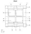
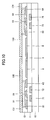
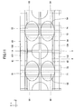
- FIG. 10 is a plan view illustrating four pixels of an active matrix substrate according to an embodiment of the present invention.
- an active matrix substrate includes plural pixels arranged in a matrix form. At least one of a source electrode, a gate electrode, and a capacitor electrode of pixel component electrodes of each of the pixels is shared by the adjacent pixels. Corresponding to at least one of the source electrode, the gate electrode, and the capacitor electrode shared by the adjacent pixels, at least one of a source signal line, a gate signal line, and a common signal line may be shared by two adjacent pixel columns or pixel rows. Furthermore, a semiconductor and/or a through hole formed in an insulation film may be shared by the two - four adjacent pixels.
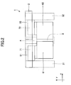
- FIG. 2 illustrates an active matrix substrate 1 of a first embodiment.
- FIG. 2 is a plan view showing signal lines and electrodes of two pixels of the active matrix substrate 1.
- source electrodes 51 and 52 and drain electrodes 61 and 62 forming an upper layer at cross section are shown by solid lines
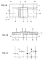
- gate electrodes 71 and 72 and a capacitor electrode 8 forming a lower layer are shown by dotted lines as in FIG. 1A .
- Semiconductors that are disposed at the upper side of the gate electrodes 71 and 72 and configured to supply currents to the drain electrodes 61 and 62 from the source electrodes 51 and 52 in response to signals from the gate electrodes 71 and 72, respectively, are not shown for the sake of simplicity.
- variable wettability material was applied onto the entire surface of a substrate using, for example, a spin-coating method and is dried to form an under layer on the substrate.
- the variable wettability material has wettability with respect to a functional liquid (described below) that varies in response to application of energy to the variable wettability material.
- the wettability as used here indicates how well the material repels or associates with the functional liquid.
- the material is in a functional liquid repelling condition when the contact angle is great, but is in a functional liquid wetting condition when the contact angle is small.
- the variable wettability material is a high-polymer material that has a hydrophobic group in a side chain forming a polymeric molecule.
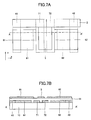
- semiconductors 9 and 91 were formed on top of the two types of multilayer structures to form the active matrix substrates shown in FIGS. 8A and 8B and FIGS. 16A - 16C , respectively.
- an inkjet method was used for device isolation of the semiconductors 91 and 91.
- the inkjet method may preferably used to achieve a perfect circle or a shape close to an ellipse utilizing aggregation of droplets due to surface tension.
Landscapes
- Devices For Indicating Variable Information By Combining Individual Elements (AREA)
- Liquid Crystal (AREA)
- Thin Film Transistor (AREA)
- Electrodes Of Semiconductors (AREA)
- Internal Circuitry In Semiconductor Integrated Circuit Devices (AREA)
Priority Applications (1)
| Application Number | Priority Date | Filing Date | Title |
|---|---|---|---|
| EP10005362.8A EP2214207A3 (fr) | 2007-10-17 | 2008-10-10 | Substrat de matrice active et dispositif d'affichage électronique |
Applications Claiming Priority (1)
| Application Number | Priority Date | Filing Date | Title |
|---|---|---|---|
| JP2007270023A JP5251068B2 (ja) | 2007-10-17 | 2007-10-17 | アクティブマトリクス基板及び電子表示装置 |
Related Child Applications (2)
| Application Number | Title | Priority Date | Filing Date |
|---|---|---|---|
| EP10005362.8A Division EP2214207A3 (fr) | 2007-10-17 | 2008-10-10 | Substrat de matrice active et dispositif d'affichage électronique |
| EP10005362.8 Division-Into | 2010-05-21 |
Publications (2)
| Publication Number | Publication Date |
|---|---|
| EP2051302A1 true EP2051302A1 (fr) | 2009-04-22 |
| EP2051302B1 EP2051302B1 (fr) | 2010-07-07 |
Family
ID=40148357
Family Applications (2)
| Application Number | Title | Priority Date | Filing Date |
|---|---|---|---|
| EP10005362.8A Withdrawn EP2214207A3 (fr) | 2007-10-17 | 2008-10-10 | Substrat de matrice active et dispositif d'affichage électronique |
| EP08253312A Ceased EP2051302B1 (fr) | 2007-10-17 | 2008-10-10 | Substrat de matrice active et dispositif d'affichage électronique |
Family Applications Before (1)
| Application Number | Title | Priority Date | Filing Date |
|---|---|---|---|
| EP10005362.8A Withdrawn EP2214207A3 (fr) | 2007-10-17 | 2008-10-10 | Substrat de matrice active et dispositif d'affichage électronique |
Country Status (5)
| Country | Link |
|---|---|
| US (1) | US20090103036A1 (fr) |
| EP (2) | EP2214207A3 (fr) |
| JP (1) | JP5251068B2 (fr) |
| DE (1) | DE602008001700D1 (fr) |
| TW (1) | TWI382375B (fr) |
Families Citing this family (14)
| Publication number | Priority date | Publication date | Assignee | Title |
|---|---|---|---|---|
| JP5376287B2 (ja) * | 2008-08-06 | 2013-12-25 | セイコーエプソン株式会社 | 回路基板、電気光学装置、電子機器 |
| JP5899606B2 (ja) * | 2010-03-04 | 2016-04-06 | 株式会社リコー | 積層構造体の製造方法 |
| JP5978577B2 (ja) | 2011-09-16 | 2016-08-24 | 株式会社リコー | 多層配線基板 |
| US20140152171A1 (en) * | 2011-09-29 | 2014-06-05 | Panasonic Corporation | Display panel and method for manufacturing same |
| JP6225511B2 (ja) * | 2013-07-02 | 2017-11-08 | セイコーエプソン株式会社 | 表示装置及び電子機器 |
| JP6436209B2 (ja) * | 2017-10-05 | 2018-12-12 | セイコーエプソン株式会社 | 表示装置及び電子機器 |
| TWI688812B (zh) * | 2018-11-21 | 2020-03-21 | 友達光電股份有限公司 | 顯示裝置 |
| JP7467976B2 (ja) * | 2019-03-04 | 2024-04-16 | 東レ株式会社 | 薄膜トランジスタ、その製造方法、ならびにそれを備えた半導体装置 |
| EP3712695B1 (fr) | 2019-03-20 | 2022-02-23 | Ricoh Company, Ltd. | Dispositif électrochromique, dispositif portable et procédé de commande d'un dispositif électrochromique |
| CN112530374B (zh) * | 2019-04-04 | 2022-04-19 | 上海中航光电子有限公司 | 驱动电路及其驱动方法、面板及其驱动方法 |
| CN209912874U (zh) | 2019-08-05 | 2020-01-07 | 北京京东方技术开发有限公司 | 显示基板、显示装置 |
| EP3835859B1 (fr) | 2019-11-29 | 2026-01-28 | Ricoh Company, Ltd. | Élément électrochromique, son procédé de fabrication et élément électrochromique d'ajustement de lumière |
| JP7472705B2 (ja) | 2020-07-29 | 2024-04-23 | 株式会社リコー | エレクトロクロミック素子、エレクトロクロミック調光素子、及びエレクトロクロミック装置 |
| WO2022246631A1 (fr) * | 2021-05-25 | 2022-12-01 | 京东方科技集团股份有限公司 | Circuit de pixels et procédé d'attaque associé et appareil d'affichage |
Citations (8)
| Publication number | Priority date | Publication date | Assignee | Title |
|---|---|---|---|---|
| JPH0333724A (ja) | 1989-06-30 | 1991-02-14 | Hitachi Ltd | 液晶表示装置 |
| US20030173629A1 (en) * | 2002-03-15 | 2003-09-18 | Masahito Gotoh | Semiconductor apparatus |
| US20040001167A1 (en) * | 2002-06-17 | 2004-01-01 | Sharp Kabushiki Kaisha | Liquid crystal display device |
| JP2005012181A (ja) * | 2003-05-28 | 2005-01-13 | Seiko Epson Corp | パターン形成方法、デバイス及びデバイスの製造方法、電気光学装置、電子機器並びにアクティブマトリクス基板の製造方法 |
| JP2005310962A (ja) * | 2003-06-02 | 2005-11-04 | Ricoh Co Ltd | 積層構造体、積層構造体を用いた電子素子、これらの製造方法、電子素子アレイ及び表示装置 |
| WO2006064443A2 (fr) * | 2004-12-16 | 2006-06-22 | Koninklijke Philips Electronics N.V. | Panneau d'affichage et procede de fabrication du panneau |
| JP2006343768A (ja) * | 2006-07-24 | 2006-12-21 | Seiko Epson Corp | 表示装置 |
| US20070164282A1 (en) * | 2006-01-18 | 2007-07-19 | Seiko Epson Corporation | Electrooptic device, method for manufacturing the same, and conductive-layer connection structure |
Family Cites Families (17)
| Publication number | Priority date | Publication date | Assignee | Title |
|---|---|---|---|---|
| JP3231261B2 (ja) * | 1997-03-26 | 2001-11-19 | 株式会社アドバンスト・ディスプレイ | 液晶表示素子及びこれを用いた液晶表示装置 |
| JP4963145B2 (ja) | 2000-05-18 | 2012-06-27 | 株式会社半導体エネルギー研究所 | 電子装置及び電子機器 |
| JP3998470B2 (ja) * | 2000-12-25 | 2007-10-24 | 川崎マイクロエレクトロニクス株式会社 | 液晶表示装置および表示システム |
| JP3946547B2 (ja) * | 2001-06-05 | 2007-07-18 | シャープ株式会社 | アクティブマトリクス基板および表示装置ならびに検出装置 |
| JP4325479B2 (ja) * | 2003-07-17 | 2009-09-02 | セイコーエプソン株式会社 | 有機トランジスタの製造方法、アクティブマトリクス装置の製造方法、表示装置の製造方法および電子機器の製造方法 |
| JP4590839B2 (ja) * | 2003-08-01 | 2010-12-01 | ソニー株式会社 | 半導体基板、液晶表示装置及びプロジェクタ |
| JP4940532B2 (ja) * | 2003-09-25 | 2012-05-30 | カシオ計算機株式会社 | Cmosトランジスタの製造方法 |
| JP4712397B2 (ja) * | 2004-01-14 | 2011-06-29 | 株式会社半導体エネルギー研究所 | 表示装置 |
| KR101192973B1 (ko) * | 2004-03-19 | 2012-10-24 | 가부시키가이샤 한도오따이 에네루기 켄큐쇼 | 패턴 형성 방법, 박막 트랜지스터, 표시 장치 및 그 제조 방법과, 텔레비전 장치 |
| EP2230551A3 (fr) * | 2004-10-06 | 2012-05-09 | Sharp Kabushiki Kaisha | Ecran à cristaux liquides |
| JP2006251120A (ja) * | 2005-03-09 | 2006-09-21 | Seiko Epson Corp | 画素構造、アクティブマトリクス基板、アクティブマトリクス基板の製造方法、電気光学装置、並びに電子機器 |
| JP2007177179A (ja) * | 2005-12-28 | 2007-07-12 | Fujifilm Corp | インク、カラーフィルタ及びその製造方法、並びに表示装置 |
| JP2007243081A (ja) * | 2006-03-13 | 2007-09-20 | Hitachi Ltd | 薄膜トランジスタ基板及び薄膜トランジスタ基板の生成方法 |
| JP5369367B2 (ja) * | 2006-03-28 | 2013-12-18 | 凸版印刷株式会社 | 薄膜トランジスタおよびその製造方法 |
| US8189141B2 (en) * | 2006-06-02 | 2012-05-29 | Semiconductor Energy Laboratory Co., Ltd. | Semiconductor device |
| JP5167707B2 (ja) * | 2006-08-04 | 2013-03-21 | 株式会社リコー | 積層構造体、多層配線基板、アクティブマトリックス基板、並びに電子表示装置 |
| JP4389978B2 (ja) * | 2007-07-06 | 2009-12-24 | ソニー株式会社 | 表示装置および表示装置の製造方法 |
-
2007
- 2007-10-17 JP JP2007270023A patent/JP5251068B2/ja not_active Expired - Fee Related
-
2008
- 2008-10-07 US US12/246,720 patent/US20090103036A1/en not_active Abandoned
- 2008-10-08 TW TW097138738A patent/TWI382375B/zh not_active IP Right Cessation
- 2008-10-10 DE DE602008001700T patent/DE602008001700D1/de active Active
- 2008-10-10 EP EP10005362.8A patent/EP2214207A3/fr not_active Withdrawn
- 2008-10-10 EP EP08253312A patent/EP2051302B1/fr not_active Ceased
Patent Citations (8)
| Publication number | Priority date | Publication date | Assignee | Title |
|---|---|---|---|---|
| JPH0333724A (ja) | 1989-06-30 | 1991-02-14 | Hitachi Ltd | 液晶表示装置 |
| US20030173629A1 (en) * | 2002-03-15 | 2003-09-18 | Masahito Gotoh | Semiconductor apparatus |
| US20040001167A1 (en) * | 2002-06-17 | 2004-01-01 | Sharp Kabushiki Kaisha | Liquid crystal display device |
| JP2005012181A (ja) * | 2003-05-28 | 2005-01-13 | Seiko Epson Corp | パターン形成方法、デバイス及びデバイスの製造方法、電気光学装置、電子機器並びにアクティブマトリクス基板の製造方法 |
| JP2005310962A (ja) * | 2003-06-02 | 2005-11-04 | Ricoh Co Ltd | 積層構造体、積層構造体を用いた電子素子、これらの製造方法、電子素子アレイ及び表示装置 |
| WO2006064443A2 (fr) * | 2004-12-16 | 2006-06-22 | Koninklijke Philips Electronics N.V. | Panneau d'affichage et procede de fabrication du panneau |
| US20070164282A1 (en) * | 2006-01-18 | 2007-07-19 | Seiko Epson Corporation | Electrooptic device, method for manufacturing the same, and conductive-layer connection structure |
| JP2006343768A (ja) * | 2006-07-24 | 2006-12-21 | Seiko Epson Corp | 表示装置 |
Also Published As
| Publication number | Publication date |
|---|---|
| TW200933560A (en) | 2009-08-01 |
| TWI382375B (zh) | 2013-01-11 |
| JP2009098418A (ja) | 2009-05-07 |
| US20090103036A1 (en) | 2009-04-23 |
| EP2214207A3 (fr) | 2015-07-08 |
| DE602008001700D1 (de) | 2010-08-19 |
| EP2051302B1 (fr) | 2010-07-07 |
| EP2214207A2 (fr) | 2010-08-04 |
| JP5251068B2 (ja) | 2013-07-31 |
Similar Documents
| Publication | Publication Date | Title |
|---|---|---|
| EP2051302B1 (fr) | Substrat de matrice active et dispositif d'affichage électronique | |
| KR100900014B1 (ko) | 적층 구조체 및 그 제조방법, 다층 회로 기판, 액티브매트릭스 기판 및 전자 표시장치 | |
| CN1286666C (zh) | 基材上图案层的制作方法 | |
| US9153524B2 (en) | Method of forming stacked-layer wiring, stacked-layer wiring, and electronic element | |
| US8598570B2 (en) | Organic transistor array, display device and method of fabricating display device | |
| KR101052578B1 (ko) | 유기 트랜지스터, 유기 트랜지스터 어레이 및 디스플레이 장치 | |
| US8097488B2 (en) | Method for forming pattern, method for manufacturing semiconductor apparatus, and method for manufacturing display | |
| US8723193B2 (en) | Multi-layer wiring substrate, active matrix substrate, image display apparatus using the same, and multi-layer wiring substrate manufacturing method | |
| KR20100022110A (ko) | 적층 구조체, 전자 소자, 및 표시 장치 | |
| US9041123B2 (en) | Thin film transistors and high fill factor pixel circuits and methods for forming same | |
| JP2004297011A (ja) | 有機トランジスタの製造方法、及び有機el表示装置の製造方法 | |
| JP2013016773A (ja) | 配線部材、および、電子素子の製造方法と、それを用いた配線部材、積層配線、電子素子、電子素子アレイ及び表示装置。 | |
| KR20140026422A (ko) | 픽셀 커패시터 | |
| US8101945B2 (en) | Laminated structure, forming method of the same, wiring board, matrix substrate and electronic display apparatus | |
| KR20060015270A (ko) | 반도체 장치용 구조체, 반도체 장치 제조 방법, 전자디바이스 및 전계발광 디바이스 | |
| JP5899606B2 (ja) | 積層構造体の製造方法 | |
| JP2009272437A (ja) | 積層構造体、半導体装置、積層構造体の製造方法及び半導体装置の製造方法 | |
| JP5412765B2 (ja) | 積層構造体、多層配線基板、アクティブマトリックス基板、画像表示装置及び積層構造体の製造方法 | |
| JP6331644B2 (ja) | 薄膜トランジスタアレイおよびその製造方法 | |
| JP6995333B2 (ja) | アクティブマトリクス基板およびアクティブマトリクス基板の製造方法 |
Legal Events
| Date | Code | Title | Description |
|---|---|---|---|
| PUAI | Public reference made under article 153(3) epc to a published international application that has entered the european phase |
Free format text: ORIGINAL CODE: 0009012 |
|
| 17P | Request for examination filed |
Effective date: 20081025 |
|
| AK | Designated contracting states |
Kind code of ref document: A1 Designated state(s): AT BE BG CH CY CZ DE DK EE ES FI FR GB GR HR HU IE IS IT LI LT LU LV MC MT NL NO PL PT RO SE SI SK TR |
|
| AX | Request for extension of the european patent |
Extension state: AL BA MK RS |
|
| 17Q | First examination report despatched |
Effective date: 20090626 |
|
| AKX | Designation fees paid |
Designated state(s): DE ES FR GB IT NL |
|
| GRAP | Despatch of communication of intention to grant a patent |
Free format text: ORIGINAL CODE: EPIDOSNIGR1 |
|
| GRAS | Grant fee paid |
Free format text: ORIGINAL CODE: EPIDOSNIGR3 |
|
| GRAA | (expected) grant |
Free format text: ORIGINAL CODE: 0009210 |
|
| AK | Designated contracting states |
Kind code of ref document: B1 Designated state(s): DE ES FR GB IT NL |
|
| REG | Reference to a national code |
Ref country code: GB Ref legal event code: FG4D |
|
| REF | Corresponds to: |
Ref document number: 602008001700 Country of ref document: DE Date of ref document: 20100819 Kind code of ref document: P |
|
| REG | Reference to a national code |
Ref country code: NL Ref legal event code: VDEP Effective date: 20100707 |
|
| PG25 | Lapsed in a contracting state [announced via postgrant information from national office to epo] |
Ref country code: NL Free format text: LAPSE BECAUSE OF FAILURE TO SUBMIT A TRANSLATION OF THE DESCRIPTION OR TO PAY THE FEE WITHIN THE PRESCRIBED TIME-LIMIT Effective date: 20100707 |
|
| PLBE | No opposition filed within time limit |
Free format text: ORIGINAL CODE: 0009261 |
|
| STAA | Information on the status of an ep patent application or granted ep patent |
Free format text: STATUS: NO OPPOSITION FILED WITHIN TIME LIMIT |
|
| PG25 | Lapsed in a contracting state [announced via postgrant information from national office to epo] |
Ref country code: IT Free format text: LAPSE BECAUSE OF FAILURE TO SUBMIT A TRANSLATION OF THE DESCRIPTION OR TO PAY THE FEE WITHIN THE PRESCRIBED TIME-LIMIT Effective date: 20100707 |
|
| 26N | No opposition filed |
Effective date: 20110408 |
|
| PG25 | Lapsed in a contracting state [announced via postgrant information from national office to epo] |
Ref country code: ES Free format text: LAPSE BECAUSE OF FAILURE TO SUBMIT A TRANSLATION OF THE DESCRIPTION OR TO PAY THE FEE WITHIN THE PRESCRIBED TIME-LIMIT Effective date: 20101018 |
|
| REG | Reference to a national code |
Ref country code: DE Ref legal event code: R097 Ref document number: 602008001700 Country of ref document: DE Effective date: 20110408 |
|
| REG | Reference to a national code |
Ref country code: FR Ref legal event code: PLFP Year of fee payment: 8 |
|
| REG | Reference to a national code |
Ref country code: FR Ref legal event code: PLFP Year of fee payment: 9 |
|
| REG | Reference to a national code |
Ref country code: FR Ref legal event code: PLFP Year of fee payment: 10 |
|
| REG | Reference to a national code |
Ref country code: FR Ref legal event code: PLFP Year of fee payment: 11 |
|
| PGFP | Annual fee paid to national office [announced via postgrant information from national office to epo] |
Ref country code: DE Payment date: 20201022 Year of fee payment: 13 Ref country code: GB Payment date: 20201022 Year of fee payment: 13 Ref country code: FR Payment date: 20201022 Year of fee payment: 13 |
|
| REG | Reference to a national code |
Ref country code: DE Ref legal event code: R119 Ref document number: 602008001700 Country of ref document: DE |
|
| GBPC | Gb: european patent ceased through non-payment of renewal fee |
Effective date: 20211010 |
|
| PG25 | Lapsed in a contracting state [announced via postgrant information from national office to epo] |
Ref country code: GB Free format text: LAPSE BECAUSE OF NON-PAYMENT OF DUE FEES Effective date: 20211010 Ref country code: DE Free format text: LAPSE BECAUSE OF NON-PAYMENT OF DUE FEES Effective date: 20220503 |
|
| PG25 | Lapsed in a contracting state [announced via postgrant information from national office to epo] |
Ref country code: FR Free format text: LAPSE BECAUSE OF NON-PAYMENT OF DUE FEES Effective date: 20211031 |