EP2059018B1 - Bildlesevorrichtung - Google Patents
Bildlesevorrichtung Download PDFInfo
- Publication number
- EP2059018B1 EP2059018B1 EP08253653.3A EP08253653A EP2059018B1 EP 2059018 B1 EP2059018 B1 EP 2059018B1 EP 08253653 A EP08253653 A EP 08253653A EP 2059018 B1 EP2059018 B1 EP 2059018B1
- Authority
- EP
- European Patent Office
- Prior art keywords
- data
- image reading
- read
- line
- image
- Prior art date
- Legal status (The legal status is an assumption and is not a legal conclusion. Google has not performed a legal analysis and makes no representation as to the accuracy of the status listed.)
- Not-in-force
Links
Images



Classifications
-
- H—ELECTRICITY
- H04—ELECTRIC COMMUNICATION TECHNIQUE
- H04N—PICTORIAL COMMUNICATION, e.g. TELEVISION
- H04N1/00—Scanning, transmission or reproduction of documents or the like, e.g. facsimile transmission; Details thereof
- H04N1/04—Scanning arrangements, i.e. arrangements for the displacement of active reading or reproducing elements relative to the original or reproducing medium, or vice versa
- H04N1/19—Scanning arrangements, i.e. arrangements for the displacement of active reading or reproducing elements relative to the original or reproducing medium, or vice versa using multi-element arrays
- H04N1/191—Scanning arrangements, i.e. arrangements for the displacement of active reading or reproducing elements relative to the original or reproducing medium, or vice versa using multi-element arrays the array comprising a one-dimensional [1D] array
- H04N1/1911—Simultaneously or substantially simultaneously scanning picture elements on more than one main scanning line, e.g. scanning in swaths
- H04N1/1912—Scanning main scanning lines which are spaced apart from one another in the sub-scanning direction
-
- H—ELECTRICITY
- H04—ELECTRIC COMMUNICATION TECHNIQUE
- H04N—PICTORIAL COMMUNICATION, e.g. TELEVISION
- H04N1/00—Scanning, transmission or reproduction of documents or the like, e.g. facsimile transmission; Details thereof
- H04N1/04—Scanning arrangements, i.e. arrangements for the displacement of active reading or reproducing elements relative to the original or reproducing medium, or vice versa
- H04N1/19—Scanning arrangements, i.e. arrangements for the displacement of active reading or reproducing elements relative to the original or reproducing medium, or vice versa using multi-element arrays
- H04N1/191—Scanning arrangements, i.e. arrangements for the displacement of active reading or reproducing elements relative to the original or reproducing medium, or vice versa using multi-element arrays the array comprising a one-dimensional [1D] array
- H04N1/1911—Simultaneously or substantially simultaneously scanning picture elements on more than one main scanning line, e.g. scanning in swaths
- H04N1/1916—Simultaneously or substantially simultaneously scanning picture elements on more than one main scanning line, e.g. scanning in swaths using an array of elements displaced from one another in the main scan direction, e.g. a diagonally arranged array
- H04N1/1917—Staggered element array, e.g. arrays with elements arranged in a zigzag
-
- H—ELECTRICITY
- H04—ELECTRIC COMMUNICATION TECHNIQUE
- H04N—PICTORIAL COMMUNICATION, e.g. TELEVISION
- H04N1/00—Scanning, transmission or reproduction of documents or the like, e.g. facsimile transmission; Details thereof
- H04N1/46—Colour picture communication systems
- H04N1/48—Picture signal generators
- H04N1/482—Picture signal generators using the same detector device sequentially for different colour components
- H04N1/484—Picture signal generators using the same detector device sequentially for different colour components with sequential colour illumination of the original
Definitions
- the present invention relates to an image reading apparatus with respect to a combination of read data between a plurality of image reading sensor units.
- the present invention relates to an image reading apparatus in which a plurality of image reading sensor units are arranged in a zigzag manner.
- JP 62-258553 A a conventional technology for correcting the amount of shift in a direction orthogonal to an arrangement direction of sensor arrays arranged in a zigzag manner is disclosed in JP 62-258553 A .
- storing means having a data storage region corresponding to each of the sensor arrays is used and read data is stored in a storage region designated by an address determined based on the amount of shift.
- Circular addressing is used for memory saving.
- the correction is performed in a unit of line for each of the sensor arrays arranged in the zigzag manner, and hence no adjustment is performed based on a distance equal to or shorter than a distance between lines.
- a color reading apparatus for successively reading respective red, green, and blue colors in each line while a document is continuously conveyed
- only the adjustment performed merely in a unit of line as in the conventional technology may cause a color shift.
- the continuously conveyed document is to be subjected to color reading
- the red, green, and blue colors are read for each line in order. Therefore, a read timing is shifted among the red, green, and blue colors.
- data is read at different timings among the respective sensor arrays.
- a read color may be different from a corresponding color of the document, and hence the accurate color of the document cannot be reproduced.
- EP 1 806 913 discloses a document reader comprising photoelectric conversion elements of line sensors arranged in a zigzag manner to read a white reference plate so as to acquire a white reference read value A.
- a white reference read average value AA is determined from the white reference read value A for each line sensor.
- the photoelectric conversion elements read another white reference plate placed on a document support plate to acquire a white reference read value B, and a white reference read average value BB is determined from the white reference read value B for each of the line sensors.
- a sensitivity offset coefficient C used for equalising the sensitivities of the sensors, which differ because of the variation of the distances from the line sensors to the document support plate, is determined by dividing the average value BB in a data processing section for each of the photoelectric conversion elements of the line sensors.
- a white reference read value Aa acquired by reading a white reference plate immediately before reading a document and a black reference read value a white reference read value Aa for shading correction of a document read value E is corrected with the sensitivity offset coefficient C.
- an image reading apparatus as defined in claim 1.
- the digital data obtained by reading by the image reading units are stored in the memory in synchronization with the read timings of the image reading units.
- the offset value is determined based on an interval between a reference image reading unit which is one of the image reading units arranged in the zigzag manner and another one of the image reading units.
- the color data has at least three values corresponding to three colors of red, green, and blue; and the read period data has at least four values, larger than the number of colors recognized by the color data, and is set to a value such that the digital data obtained by reading does not overlap with data of preceding and succeeding read lines.
- the image data obtained by reading the colors on the, same line can be read without errors. Therefore, the image data faithfully reproducing the read document can be obtained.
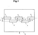
- Fig. 1 is an arrangement diagram showing image reading units.
- a contact image sensor unit is used as each of the image reading units.
- the contact image sensor unit is referred to as a CIS.
- Five CISs that is, a CIS-A 1, a CIS-B 2, a CIS-C 3, a CIS-D 4, and a CIS-E 5 are arranged in a zigzag manner to read a document 6 conveyed in a direction indicated by an arrow.
- Red, green, and blue LEDs are arranged in each of the CISs.
- the LEDs are used as light sources.
- Approximately 5,000 photoelectric conversion elements are arranged in line. Light reflected on the document 6 is subjected to photoelectric conversion to read the document, and then converted into digital data.
- the respective CISs are arranged so as to overlap with each other in a conveying direction of the document 6, thereby performing overlap reading.
- Line differences indicating the number of lines corresponding to the intervals in a case where each line of reading is set as a unit are a line difference L1, a line difference L2, a line difference L3, and a line difference L4.
- Data of the line differences are stored as line difference data in a memory.
- the line difference data are read out from the memory, and then adjacent data originally constituting one line are combined based on the line difference data.
- the image data located in positions in which the line difference data corresponding to a distance difference between the image reading units becomes 0 are combined to each other.
- Fig. 2 is a schematic view showing an image reading apparatus.
- a read portion 8 in which the five CISs are arranged in the zigzag manner is provided under a glass 9 in a case 7.
- a document base cover 13 is provided above the case 7 to block light from the outside.
- the document 6 taken into the apparatus is held by a first conveying roller pair 10 and a second conveying roller pair 11, conveyed at a constant speed, and delivered to a document outlet 12.
- the document 6 is read through the glass 9 by the read portion 8.
- the document 6 is conveyed at a constant speed and read by the document read portion 8 to generate image data.
- Fig. 3 is a block diagram showing an electrical structure of the read portion according to the present invention.
- Digital data of the document read by the respective CISs that is, the CIS-A 1, the CIS-B 2, the CIS-C 3, the CIS-D 4, and the CIS-E 5 are output to a sensor control circuit 14.
- Color type data indicating read data obtained by turning on which color LED and a value (line number) obtained by circulating a value of 1 to 4 in order for each read line are added as a header to the digital data of the read document.
- the document is periodically read, and hence the line number is used as data indicating a read period.
- a first line detection circuit 15 is a circuit for detecting data having a header predetermined with respect to data obtained by reading for each line and each color.
- An offset value memory 16 is a memory for storing line difference data corresponding to an interval between adjacent CISs of the CISs arranged in the zigzag manner.
- the sensor control circuit 14 controls the respective CISs, processes data which are read and digitized by the CISs, and writes the data into an image memory 17.
- the image memory 17 includes a sensor-A memory 18 for storing an image for the CIS-A 1, a sensor-B memory 19 for storing an image for the CIS-B 2, a sensor-C memory 20 for storing an image for the CIS-C 3, a sensor-D memory 21 for storing an image for the CIS-D 4, and a sensor-E memory 22 for storing an image for the CIS-E 5.
- An address of the image memory 17 is an address 0 to an address n.
- one-line image data read by each of the CISs is stored in a CIS memory for the corresponding CIS.
- An address control circuit 30 is a circuit for performing management and control so as to prevent an overlapped writing and overlapped reading to and from the image memory 17.
- the sensor control circuit 14 starts data writing from an address of the image memory 17 which corresponds to each of the CISs based on a value stored in the offset value memory. For example, when line difference data from a reference point in the CIS-A 1 is 500 lines, the value of the offset value memory is 500, and hence data is written for each line from an address corresponding to a 500th line counted from the address 0. For example, in Fig. 3 , an address k-1 is an address corresponding to the 500th line, and hence data is written from this address. Even in the case of each of the other CISs, data captured for each line from a position corresponding to line difference data from the reference is written. Writing of image data on each line starts from an address 1 in the CIS-B 2, from the address k-1 in the CIS-C 3, from the address 1 in the CIS-D 4, and from an address k in the CIS-E 5.
- the first line detection circuit 15 determines, of read image data, first data to be stored in a first address for data writing.
- the first line detection circuit 15 reads colors of data from the CISs and circulated line numbers, compares predetermined header values to each other to find matched data. This is to detect data for starting writing to the image memory 17. The data for starting the writing to the memory 17 and a timing thereof are determined based on the data detected by the circuit. The read image data is written for each line from a region designated by the predetermined address of the memory at the determined timing. The image memory 17 is used while an address thereof is circulated.
- An address of the image memory 17 is designated for each line. Consecutive other addresses are assigned for respective colors. For example, an address i is assigned to one-line data for red, a next address i+1 is assigned to one-line data for green, and a next address i+2 is assigned to one-line data for blue. Memory regions corresponding to three addresses are used for color to store one-line data.
- the CIS which performs final reading in the conveying direction, of the CISs arranged in the zigzag manner is the CIS corresponding to a maximum value of the offset value memory.
- one-line image data is completed.
- data stored in a region corresponding to an address m of the image memory 17 is one-line data.
- One-line data obtained by reading by each of the CISs is stored in a region corresponding to the address m of each of the sensor-A memory 18, the sensor-B memory 19, the sensor-C memory 20, the sensor-D memory 21, and the sensor-E memory 22.
- the address m is designated, data corresponding to the originally same line, which is obtained by reading by the respective CISs, can be designated.
- an overlap portion of the data in the arrangement direction of the CISs is processed.
- an overlap range is stored in advance in a combination position information memory 26.
- a combination processing circuit 25 first reads, into a one-line-combination pre-processing buffer 27, the one-line data read from the image memory 17.
- Data portions to be used, of the data from the CISs are designated based on the data of the combination position information memory 26, and hence overlap portion image data 29 which are unused portions are removed and resultant data portions are written into an one-line image data buffer 28.
- the combination processing circuit 25 When the data from all the CISs are combined, one-line image data is obtained.
- the combination processing circuit 25 successively writes the completed image data for each line into another memory to obtain read image data of the document by combination.
- the entire image data is transmitted for use to another apparatus such as a printing apparatus or an information processing apparatus.
- the image data can be transmitted to a recording medium and stored therein. Examples of the image reading apparatus include an image scanner, a copying machine, and a facsimile machine.
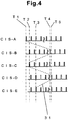
- Fig. 4 is a read timing chart of the respective CISs. Read timings of the respective CISs are shown. The respective CISs successively read respective colors of red, green, and blue on a line. Fig. 4 shows signals, each of which indicates the start of reading of each of the CISs for each line. The rising of each of the signals is detected to turn on LEDs of respective colors of red, green, and blue in order, thereby reading the document for each of the colors. This figure shows only the signals indicating the start of reading for red. The same signals are used for green and blue. The signals for each of three colors are risen at equal intervals. A signal for one of the colors is risen between the risings of signals for the others thereof.
- Reading for the respective colors is started in response to the respective signals.
- Read start signals for green and blue are omitted here.
- a signal rising interval is determined in advance such that three-color reading is completed before the next rising of the read start signal for red.
- the read timings of the respective CISs are non-synchronous.
- the rising of each of the signals as indicated by a broken line 31 in Fig. 4 is a timing for reading the originally same line.
- the respective CISs are arranged in the zigzag manner, and hence the timings are shifted correspondingly to the arrangement.
- a time T1 of the CIS-A, a time T4 of the CIS-B, a time T2 of the CIS-C, a time T5 of the CIS-D, and a time T3 of the CIS-E are read times of the respective CISs which are required to obtain the originally same line.
- the read interval is an equal interval, and hence it can be also said that the time difference exhibits the line difference among the arranged CISs.
- the amount of shift between the predetermined reference point and the originally same line to be obtained by the respective CISs, that is, the line difference data is stored in advance in the offset value memory 16.
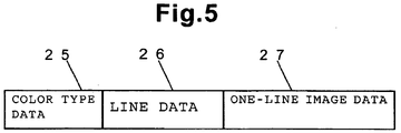
- Fig. 5 shows a structure of read data output from each of the CISs. This is data obtained by adding, to one-line image data 27 which is digital data read by the CIS, color type data 25 indicating read data obtained by turning on which color LED used as the light source and line data 26 indicating nth data, as header data.
- Three bits are used for the color type data. For example, "110" is used for red, "101” is used for green, and "011” is used for blue.
- a read color is indicated by a bit whose value is 0.
- Two bits are used for line data. Four lines are indicated by four values of "00", “01”, “10", and "11” and circulated for use. Three-color data are used for each line. Therefore, when data corresponding to four lines are used, whether data is data corresponding an adjacent line for the same color or data corresponding to the same line can be determined. When next processing is performed during this, the preceding and succeeding lines are not confused.
- Fig. 6 is a schematic explanatory diagram showing data correction after the primary correction. This shows read timings of the CISs for each line, and the color type data and the line data which are added to the read line data. Even in the following description, only a signal for red (R) is used as the read start signal. This also shows timings when image data from the respective CISs are written into the image memory 17.
- reference CIS is the CIS-A 1.
- the first line detection circuit 15 When reading for a line starts, the first line detection circuit 15 operates. Then, data from the CIS-A 1 is read and detection continues until predetermined color type data is the red color indicated by "110" and data which is the line data "10" is read. After the detection, the first line detection circuit 15 writes, into corresponding predetermined addresses of the image memory 17, read data from all the CISs on a line in which the color type data is the red color indicated by "110" and the line data is "00" after the next. Even in a case of image data on subsequent lines, the writing is performed with successive addresses in response to timings based on the read timings. For example, the writing is performed in synchronization with the read timings.
- CIS-A In the case of the CIS-A, from the rising of data capture-A, data for each line from the address k-1 of the sensor-A memory is written for each next rising of the image read interval from the rising of T6 in the CIS-A as shown in Fig. 6 .
- image data are written into the image memory 17 from predetermined addresses at predetermined timings from T7 in the CIS-B, from T8 in the CIS-D, from T9 in the CIS-E, and from T10 in the CIS-C.
- the lines to be originally combined are stored in the same address region. With respect to other read data for green and blue, data writing is performed in response to the read timings as in the case of red.
- the first line detection circuit 15 monitors the color type data and the line data which are added to the image data from the reference CIS.
- predetermined line data of predetermined color type data is detected
- the color type data and the line data which are added to the image data are monitored on read data for each line, of the respective image data from all the CISs. In this case, whether or not line data after the next of the predetermined line data of the predetermined color type data is detected is monitored.
- the image data for each line are successively stored in a region of the image memory 17 which corresponds to the CIS which detects the data, from the address determined based on the line difference data stored in the offset value memory 16.
- the read image data are stored at predetermined timings. For example, read data are stored in the memory in synchronization with the image read timings.
- the image data of the same line are stored in the same address region.
- the reason why the line data after the next of the predetermined line data of the predetermined color type data is detected is as follows. Although correction in a unit of line is performed as correction between lines, a capture period for each color is not corrected. Therefore, when a processing time is included, it is likely to cause a delay corresponding to three periods in maximum, and hence writing is started from data delayed by two periods. Thus, the writing may be performed from predetermined line data after two lines.
- timings for reading on the originally same line by the CISs are varied among the respective CISs. Therefore, an error is corrected based on the write timings to the memory 17, and hence the read data of the originally same line is accurately reproduced.
- the present invention is not limited thereto.
- the image data captured by the respective CISs on the originally same line are marked in advance with identification codes to provide a correspondence relationship among data on the originally same line.
- a method of providing an identification code for each line and a method of adding a storage address of next data to be combined can also be provided. Therefore, in order to obtain desired one-line image data the one-line image data can be obtained based on a designated address.
Landscapes
- Engineering & Computer Science (AREA)
- Multimedia (AREA)
- Signal Processing (AREA)
- Facsimile Scanning Arrangements (AREA)
- Image Input (AREA)
- Facsimile Image Signal Circuits (AREA)
- Color Image Communication Systems (AREA)
Claims (4)
- Eine Bildlesevorrichtung, in der eine Mehrzahl von Bildleseeinheiten (1-5) zum Lesen eines kontinuierlich transportierten Dokuments (6) in einer Zickzack-Anordnung angeordnet sind, wobei die Bildleseeinheiten Reflexionslicht für jede Farbe auf dem Dokument durch fotoelektrische Konversionselemente lesen, die in einer Reihe angeordnet sind, während Lichtquellen mit einer Mehrzahl von Farben sukzessive ein- und ausgeschaltet werden, um digitale Daten zu erhalten, und die digitalen Daten, die mit den jeweiligen Bildleseeinheiten assoziiert sind, kombiniert werden, um Bilddaten einer Zeile zu erhalten, dadurch gekennzeichnet, dass
die digitalen Daten jeweils Farbdaten einschließen, die eine der Farben der Lichtquellen angeben, die verwendet werden, um die digitalen Daten zu erhalten, sowie Leseperiodedaten, die eine der Erfassungsperioden der digitalen Daten angeben,
wobei die Bildlesevorrichtung aufweist:erste Bilddetektionsmittel (15) zum Detektieren, aus den digitalen Daten, die durch Lesen der Bildleseeinheiten erhalten werden, der digitalen Daten mit den Farbdaten, die eine vorbestimmte Farbe angeben und den Leseperiodedaten, die eine vorbestimmte Erfassungsperiode angeben;einen Speicher (17) einschließend eine Mehrzahl von Adressen und entsprechende Speicherregionen zum Speichern, für jede der Adresse, von digitalen Daten, die erhalten werden durch jede der Bildleseeinheiten, wobei die digitalen Daten so ermittelt werden, dass sie die gleichen Farbdaten und die gleichen Leseperiodedaten einschließen basierend auf den Ergebnissen der Detektion durch die ersten Bilddetektionsmittel für die jeweiligen Bildleseeinheiten; undBildsteuermittel (25) zum Kombinieren der digitalen Daten, die assoziiert sind mit den jeweiligen Bildleseeinheiten, welche gespeichert werden in den Speicherregionen entsprechend den Adressen aus dem Speicher, um die einzeiligen Bilddaten zu erzeugen;wobei die ersten Bilddetektionsmittel eine Detektion zu Lesezeiten der Bildleseeinheiten durchführen und ein Schreib-Timing der digitalen Daten in den Speicher für jede der Bildleseeinheiten an ein Timing anpassen basierend auf einem Lesetiming, wenn die digitalen Daten mit den vorbestimmten Farbdaten und den vorbestimmten Leseperiodedaten für diese Bildleseeinheit detektiert werden; undwobei ein Offset-Wert ermittelt wird im Voraus für jede der Bildleseeinheiten basierend auf einer gelesenen Zeilenbreite der Bildlesevorrichtung relativ zu einem Intervall in einer Transportrichtung zwischen dieser Bildleseeinheit und einem Referenzpunkt, wobei die Bildleseeinheiten in einer Zickzack-Anordnung angeordnet sind und eine Adresse zum Starten des Speicherns der digitalen Daten in den Speicher für jede Bildleseeinheit ermittelt wird basierend auf dem Offset-Wert für diese Bildleseeinheit. - Die Bildlesevorrichtung nach Anspruch 1, wobei nachdem die digitalen Daten in den Speicher zum Schreib-Timing geschrieben wurden, die digitalen Daten, die durch Lesen durch die Bildleseeinheiten erhalten wurden, gespeichert werden in dem Speicher in Synchronisation mit den Lesetimings der Bildleseeinheiten.
- Die Bildlesevorrichtung nach Anspruch 1 oder 2, wobei der Offset-Wert ermittelt wird basierend auf einem Intervall zwischen einer Referenzbildleseeinheit, die eine der in Zickzack-Anordnung angeordneten Bildleseeinheiten ist und einer anderen der Bildleseeinheiten.
- Die Bildlesevorrichtung nach einem der Ansprüche 1 bis 3, wobei
die Farbdaten zumindest drei Werten entsprechend den Farben rot, grün und blau aufweisen; und
die Leseperiodedaten zumindest vier Werte aufweisen, größer als die Anzahl der Farben, die durch die Farbdaten erkannt werden, und gesetzt werden auf einen Wert derart, dass die digitalen Daten, die durch Lesen erhalten werden, nicht überlappen mit Daten von vorhergehenden und nachfolgenden Lesezeilen.
Applications Claiming Priority (1)
| Application Number | Priority Date | Filing Date | Title |
|---|---|---|---|
| JP2007291685A JP5048459B2 (ja) | 2007-11-09 | 2007-11-09 | 画像読取装置 |
Publications (3)
| Publication Number | Publication Date |
|---|---|
| EP2059018A2 EP2059018A2 (de) | 2009-05-13 |
| EP2059018A3 EP2059018A3 (de) | 2010-04-14 |
| EP2059018B1 true EP2059018B1 (de) | 2016-04-13 |
Family
ID=40325845
Family Applications (1)
| Application Number | Title | Priority Date | Filing Date |
|---|---|---|---|
| EP08253653.3A Not-in-force EP2059018B1 (de) | 2007-11-09 | 2008-11-07 | Bildlesevorrichtung |
Country Status (3)
| Country | Link |
|---|---|
| US (1) | US8243350B2 (de) |
| EP (1) | EP2059018B1 (de) |
| JP (1) | JP5048459B2 (de) |
Families Citing this family (1)
| Publication number | Priority date | Publication date | Assignee | Title |
|---|---|---|---|---|
| JP2017163224A (ja) * | 2016-03-07 | 2017-09-14 | 株式会社東芝 | 画像処理装置 |
Family Cites Families (12)
| Publication number | Priority date | Publication date | Assignee | Title |
|---|---|---|---|---|
| JPS62258553A (ja) * | 1986-05-02 | 1987-11-11 | Canon Inc | 長尺センサのレジストレ−シヨン調整装置 |
| JP3005007B2 (ja) * | 1989-12-21 | 2000-01-31 | キヤノン株式会社 | 画像符号化装置 |
| JPH05103212A (ja) * | 1991-10-03 | 1993-04-23 | Sony Corp | データ伝送装置 |
| US6972879B2 (en) * | 2001-10-24 | 2005-12-06 | Kabushiki Kaisha Toshiba | Image scanning apparatus |
| CN2629069Y (zh) * | 2002-03-29 | 2004-07-28 | 精工爱普生株式会社 | 写入头和使用它的图像形成装置 |
| JP3743401B2 (ja) * | 2002-06-28 | 2006-02-08 | ブラザー工業株式会社 | 画像読取装置 |
| JP2006093820A (ja) * | 2004-09-21 | 2006-04-06 | Canon Inc | リニアイメージセンサ、画像読取装置、画像読取方法、及びプログラム |
| JP4567416B2 (ja) * | 2004-10-29 | 2010-10-20 | 株式会社セイコーアイ・インフォテック | 原稿読取り方法、原稿読取り装置、画像形成装置、及びイメージスキャナ |
| US7715064B2 (en) * | 2004-12-20 | 2010-05-11 | Graphtec Kabushiki Kaisha | Image reading apparatus |
| JP4712497B2 (ja) * | 2005-09-15 | 2011-06-29 | ローム株式会社 | フィルタ回路、並びに、これを用いたイメージセンサ、イメージセンサモジュール、画像読取装置 |
| JP2007267359A (ja) * | 2006-03-03 | 2007-10-11 | Ricoh Co Ltd | 画像読み取り装置及び画像形成装置 |
| KR20090014034A (ko) * | 2007-08-03 | 2009-02-06 | 삼성전자주식회사 | 잉크젯 화상형성장치 |
-
2007
- 2007-11-09 JP JP2007291685A patent/JP5048459B2/ja not_active Expired - Fee Related
-
2008
- 2008-11-06 US US12/291,093 patent/US8243350B2/en not_active Expired - Fee Related
- 2008-11-07 EP EP08253653.3A patent/EP2059018B1/de not_active Not-in-force
Also Published As
| Publication number | Publication date |
|---|---|
| EP2059018A3 (de) | 2010-04-14 |
| US8243350B2 (en) | 2012-08-14 |
| EP2059018A2 (de) | 2009-05-13 |
| JP5048459B2 (ja) | 2012-10-17 |
| JP2009118373A (ja) | 2009-05-28 |
| US20090122370A1 (en) | 2009-05-14 |
Similar Documents
| Publication | Publication Date | Title |
|---|---|---|
| US7072075B2 (en) | Image reader | |
| EP1102468B1 (de) | Bildabtastungsgerät, Bilderzeugungsgerät, Bilderzeugungssystem, Bildabtastungs-Steuerungsverfahren und Speichermedium | |
| US20070285690A1 (en) | Image processing apparatus and computer readable medium storing image processing program | |
| US20090009828A1 (en) | Original reading device and image forming apparatus | |
| US20030219170A1 (en) | Image processing method and apparatus | |
| US4926253A (en) | Multi-color document reading apparatus for facsimile and multi-color facsimile | |
| JP4567416B2 (ja) | 原稿読取り方法、原稿読取り装置、画像形成装置、及びイメージスキャナ | |
| EP2059018B1 (de) | Bildlesevorrichtung | |
| US20080024823A1 (en) | Image processing apparatus and image reading apparatus | |
| EP0504641B1 (de) | Bildlesegerät und Verfahren zum Bildlesen | |
| US6559981B1 (en) | Image reading apparatus | |
| US8339685B2 (en) | Image reading apparatus | |
| US20140063561A1 (en) | Image processing apparatus, image forming apparatus, and image processing method | |
| JP2002176542A (ja) | 画像読み取り装置及び画像読み取り方法 | |
| JP2004193742A (ja) | 画像読み取り装置、画像データ処理方法及び制御プログラム | |
| JP2002232656A (ja) | 原稿処理装置 | |
| JPS6234363Y2 (de) | ||
| JPS63202181A (ja) | ライン画信号除去方式 | |
| JP2006310897A (ja) | センサ信号処理回路装置 | |
| JPH1127454A (ja) | 原稿読取装置及び原稿読取方法及び記憶媒体 | |
| JPS6388963A (ja) | 原稿読取装置 | |
| JP2009284155A (ja) | 画像読取装置及び画像形成装置 | |
| JPH03147479A (ja) | 画像読み取り装置 | |
| JPH05336316A (ja) | 画像入出力装置 | |
| JPH11341225A (ja) | 画像読み取り装置及びその斜行補正方法 |
Legal Events
| Date | Code | Title | Description |
|---|---|---|---|
| PUAI | Public reference made under article 153(3) epc to a published international application that has entered the european phase |
Free format text: ORIGINAL CODE: 0009012 |
|
| AK | Designated contracting states |
Kind code of ref document: A2 Designated state(s): AT BE BG CH CY CZ DE DK EE ES FI FR GB GR HR HU IE IS IT LI LT LU LV MC MT NL NO PL PT RO SE SI SK TR |
|
| AX | Request for extension of the european patent |
Extension state: AL BA MK RS |
|
| PUAL | Search report despatched |
Free format text: ORIGINAL CODE: 0009013 |
|
| AK | Designated contracting states |
Kind code of ref document: A3 Designated state(s): AT BE BG CH CY CZ DE DK EE ES FI FR GB GR HR HU IE IS IT LI LT LU LV MC MT NL NO PL PT RO SE SI SK TR |
|
| AX | Request for extension of the european patent |
Extension state: AL BA MK RS |
|
| RIC1 | Information provided on ipc code assigned before grant |
Ipc: H04N 1/19 20060101AFI20090213BHEP Ipc: H04N 1/191 20060101ALI20100305BHEP |
|
| 17P | Request for examination filed |
Effective date: 20101014 |
|
| AKX | Designation fees paid |
Designated state(s): DE FR GB |
|
| 17Q | First examination report despatched |
Effective date: 20130108 |
|
| REG | Reference to a national code |
Ref country code: DE Ref legal event code: R079 Ref document number: 602008043467 Country of ref document: DE Free format text: PREVIOUS MAIN CLASS: H04N0001190000 Ipc: H04N0001191000 |
|
| GRAP | Despatch of communication of intention to grant a patent |
Free format text: ORIGINAL CODE: EPIDOSNIGR1 |
|
| RIC1 | Information provided on ipc code assigned before grant |
Ipc: H04N 1/191 20060101AFI20150922BHEP Ipc: H04N 1/48 20060101ALI20150922BHEP |
|
| INTG | Intention to grant announced |
Effective date: 20151021 |
|
| RAP1 | Party data changed (applicant data changed or rights of an application transferred) |
Owner name: OKI DATA INFOTECH CORPORATION |
|
| GRAS | Grant fee paid |
Free format text: ORIGINAL CODE: EPIDOSNIGR3 |
|
| GRAA | (expected) grant |
Free format text: ORIGINAL CODE: 0009210 |
|
| AK | Designated contracting states |
Kind code of ref document: B1 Designated state(s): DE FR GB |
|
| REG | Reference to a national code |
Ref country code: GB Ref legal event code: FG4D |
|
| REG | Reference to a national code |
Ref country code: DE Ref legal event code: R096 Ref document number: 602008043467 Country of ref document: DE |
|
| REG | Reference to a national code |
Ref country code: FR Ref legal event code: PLFP Year of fee payment: 9 |
|
| REG | Reference to a national code |
Ref country code: DE Ref legal event code: R097 Ref document number: 602008043467 Country of ref document: DE |
|
| PLBE | No opposition filed within time limit |
Free format text: ORIGINAL CODE: 0009261 |
|
| STAA | Information on the status of an ep patent application or granted ep patent |
Free format text: STATUS: NO OPPOSITION FILED WITHIN TIME LIMIT |
|
| 26N | No opposition filed |
Effective date: 20170116 |
|
| REG | Reference to a national code |
Ref country code: FR Ref legal event code: PLFP Year of fee payment: 10 |
|
| REG | Reference to a national code |
Ref country code: DE Ref legal event code: R082 Ref document number: 602008043467 Country of ref document: DE Representative=s name: BETTEN & RESCH PATENT- UND RECHTSANWAELTE PART, DE Ref country code: DE Ref legal event code: R081 Ref document number: 602008043467 Country of ref document: DE Owner name: OKI DATA CORP., JP Free format text: FORMER OWNER: OKI DATA INFOTECH CORP., CHIBA, JP |
|
| REG | Reference to a national code |
Ref country code: GB Ref legal event code: 732E Free format text: REGISTERED BETWEEN 20180607 AND 20180613 |
|
| REG | Reference to a national code |
Ref country code: FR Ref legal event code: PLFP Year of fee payment: 11 |
|
| REG | Reference to a national code |
Ref country code: FR Ref legal event code: TP Owner name: OKI DATA CORPORATION, JP Effective date: 20181001 |
|
| PGFP | Annual fee paid to national office [announced via postgrant information from national office to epo] |
Ref country code: DE Payment date: 20191022 Year of fee payment: 12 |
|
| PGFP | Annual fee paid to national office [announced via postgrant information from national office to epo] |
Ref country code: FR Payment date: 20191015 Year of fee payment: 12 |
|
| PGFP | Annual fee paid to national office [announced via postgrant information from national office to epo] |
Ref country code: GB Payment date: 20191107 Year of fee payment: 12 |
|
| REG | Reference to a national code |
Ref country code: DE Ref legal event code: R119 Ref document number: 602008043467 Country of ref document: DE |
|
| GBPC | Gb: european patent ceased through non-payment of renewal fee |
Effective date: 20201107 |
|
| PG25 | Lapsed in a contracting state [announced via postgrant information from national office to epo] |
Ref country code: FR Free format text: LAPSE BECAUSE OF NON-PAYMENT OF DUE FEES Effective date: 20201130 |
|
| PG25 | Lapsed in a contracting state [announced via postgrant information from national office to epo] |
Ref country code: GB Free format text: LAPSE BECAUSE OF NON-PAYMENT OF DUE FEES Effective date: 20201107 Ref country code: DE Free format text: LAPSE BECAUSE OF NON-PAYMENT OF DUE FEES Effective date: 20210601 |