EP2059101A2 - Stromleitungsanordnung - Google Patents
Stromleitungsanordnung Download PDFInfo
- Publication number
- EP2059101A2 EP2059101A2 EP08019262A EP08019262A EP2059101A2 EP 2059101 A2 EP2059101 A2 EP 2059101A2 EP 08019262 A EP08019262 A EP 08019262A EP 08019262 A EP08019262 A EP 08019262A EP 2059101 A2 EP2059101 A2 EP 2059101A2
- Authority
- EP
- European Patent Office
- Prior art keywords
- power line
- power
- lines
- power lines
- sub
- Prior art date
- Legal status (The legal status is an assumption and is not a legal conclusion. Google has not performed a legal analysis and makes no representation as to the accuracy of the status listed.)
- Granted
Links
Images




Classifications
-
- H—ELECTRICITY
- H01—ELECTRIC ELEMENTS
- H01R—ELECTRICALLY-CONDUCTIVE CONNECTIONS; STRUCTURAL ASSOCIATIONS OF A PLURALITY OF MUTUALLY-INSULATED ELECTRICAL CONNECTING ELEMENTS; COUPLING DEVICES; CURRENT COLLECTORS
- H01R13/00—Details of coupling devices of the kinds covered by groups H01R12/70 or H01R24/00 - H01R33/00
- H01R13/646—Details of coupling devices of the kinds covered by groups H01R12/70 or H01R24/00 - H01R33/00 specially adapted for high-frequency, e.g. structures providing an impedance match or phase match
-
- H—ELECTRICITY
- H05—ELECTRIC TECHNIQUES NOT OTHERWISE PROVIDED FOR
- H05K—PRINTED CIRCUITS; CASINGS OR CONSTRUCTIONAL DETAILS OF ELECTRIC APPARATUS; MANUFACTURE OF ASSEMBLAGES OF ELECTRICAL COMPONENTS
- H05K1/00—Printed circuits
- H05K1/02—Details
- H05K1/0213—Electrical arrangements not otherwise provided for
- H05K1/0216—Reduction of cross-talk, noise or electromagnetic interference
- H05K1/0228—Compensation of cross-talk by a mutually correlated lay-out of printed circuit traces, e.g. for compensation of cross-talk in mounted connectors
-
- G—PHYSICS
- G05—CONTROLLING; REGULATING
- G05F—SYSTEMS FOR REGULATING ELECTRIC OR MAGNETIC VARIABLES
- G05F1/00—Automatic systems in which deviations of an electric quantity from one or more predetermined values are detected at the output of the system and fed back to a device within the system to restore the detected quantity to its predetermined value or values, i.e. retroactive systems
- G05F1/10—Regulating voltage or current
-
- H—ELECTRICITY
- H02—GENERATION; CONVERSION OR DISTRIBUTION OF ELECTRIC POWER
- H02M—APPARATUS FOR CONVERSION BETWEEN AC AND AC, BETWEEN AC AND DC, OR BETWEEN DC AND DC, AND FOR USE WITH MAINS OR SIMILAR POWER SUPPLY SYSTEMS; CONVERSION OF DC OR AC INPUT POWER INTO SURGE OUTPUT POWER; CONTROL OR REGULATION THEREOF
- H02M1/00—Details of apparatus for conversion
- H02M1/12—Arrangements for reducing harmonics from AC input or output
-
- H—ELECTRICITY
- H05—ELECTRIC TECHNIQUES NOT OTHERWISE PROVIDED FOR
- H05K—PRINTED CIRCUITS; CASINGS OR CONSTRUCTIONAL DETAILS OF ELECTRIC APPARATUS; MANUFACTURE OF ASSEMBLAGES OF ELECTRICAL COMPONENTS
- H05K1/00—Printed circuits
- H05K1/02—Details
- H05K1/0213—Electrical arrangements not otherwise provided for
- H05K1/0237—High frequency adaptations
- H05K1/0245—Lay-out of balanced signal pairs, e.g. differential lines or twisted lines
-
- H—ELECTRICITY
- H05—ELECTRIC TECHNIQUES NOT OTHERWISE PROVIDED FOR
- H05K—PRINTED CIRCUITS; CASINGS OR CONSTRUCTIONAL DETAILS OF ELECTRIC APPARATUS; MANUFACTURE OF ASSEMBLAGES OF ELECTRICAL COMPONENTS
- H05K2201/00—Indexing scheme relating to printed circuits covered by H05K1/00
- H05K2201/09—Shape and layout
- H05K2201/09209—Shape and layout details of conductors
- H05K2201/09218—Conductive traces
- H05K2201/09263—Meander
-
- H—ELECTRICITY
- H05—ELECTRIC TECHNIQUES NOT OTHERWISE PROVIDED FOR
- H05K—PRINTED CIRCUITS; CASINGS OR CONSTRUCTIONAL DETAILS OF ELECTRIC APPARATUS; MANUFACTURE OF ASSEMBLAGES OF ELECTRICAL COMPONENTS
- H05K2201/00—Indexing scheme relating to printed circuits covered by H05K1/00
- H05K2201/09—Shape and layout
- H05K2201/09209—Shape and layout details of conductors
- H05K2201/09654—Shape and layout details of conductors covering at least two types of conductors provided for in H05K2201/09218 - H05K2201/095
- H05K2201/097—Alternating conductors, e.g. alternating different shaped pads, twisted pairs; Alternating components
Definitions
- One or more embodiments described herein relate to power lines.
- Common-mode noise can radiate from a power line between inputs of board-mounted devices and ground.
- Common-mode noise is a leading cause electromagnetic interference (EMI), which propagates between devices along power and other circuit lines.
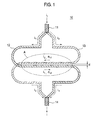
- Figure 1 is a diagram of one embodiment of a power line arrangement.
- Figure 2 is a conceptual diagram illustrating a principle of noise reduction that may be achieved in the power line arrangement of Figure 1 .
- Figure 3A shows an EMI radiation pattern on another type of power line
- Figure 3B shows and an EMI radiation pattern that may be generated by the power line arrangement of Figure 1 .
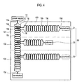
- Figure 4 is a diagram showing one arrangement of connections between one or more power lines formed according to the embodiment of Figure 1 and other electronic devices.
- Figure 5 is a diagram showing another arrangement of connections between one or more power lines formed according to the embodiment of Figure 1 and other electronic devices.
- Figure. 6 is a diagram showing another arrangement of connections between one or more power lines formed according to the embodiment of Figure 1 and other electronic devices.
- Figure 1 shows one embodiment of a power line 10 having two ends 11 and 14. From end 11, a pair of power lines 12 and 13 branch off and extend in different (e.g., opposing) directions. Power lines 12 and 13 may have one or more common properties, e.g., resistance. As further shown in Figure 1 , at least one cross area A is formed between power lines 12 and 13. The directions in which current flows in the power lines may be different. This may be accomplished by aligning the power lines in a manner which allows the different current directions to be formed at the cross area. Also, power lines 12 and 13 may be aligned in two or three dimensions so as to form opposing current directions at the cross area.
- the power lines may have a chain or twist shape but they do not necessarily contact each other in this area.
- power lines 12 and 13 branch off from end 11, meet at cross area A, and extend away again to escape the cross area A.
- the two power lines meet and are coupled, for example, to a power input of an electronic device element or are grounded.
- end 11 of power line 10 is coupled to a direct current (DC) power supply.
- DC direct current
- noise components e.g., common-mode noise and EMI
- Figure 2 illustrates one principle of how noise (and EMI) can be reduced or eliminated in the power line of Figure 1 .
- the direction of current i 1 flowing through power line 12 in cross area A is defined as the "+" direction
- the direction of current i 2 flowing through power line 13 has an opposite direction, i.e., the "-" direction.
- common-mode noise components n 21 and n 12 are generated on/by power lines 12 and 13, respectively, due to currents i 2 and i 1 . That is, common-mode noise component n 21 generated by current i 2 flowing through power line 13 is induced on power line 12, through which current i 1 flows.
- common-mode noise component n 12 generated by current i 1 through power line 13 is induced on second power line 13, through which current i 2 flows. Because these noise-components are equal (or at least substantially so) and opposite, they reduce or cancel one another out in each power line.
- n 12 k ⁇ n c ⁇ 1
- coupling coefficient "k” depends on the widths of and distances between the power lines.
- the coupling coefficient k may be arbitrarily set within a range from 0 to 1 (0 ⁇ k ⁇ 1).
- the coupling coefficient k may be set to become larger.
- the distance between the lines may have more effect on the coupling coefficient than the widths of the lines.
- n r2 1 - k ⁇ n c ⁇ 2
- power line 10 may have a plurality of cross areas.
- noise reduction or elimination results in each cross area based on the aforementioned principles.
- N cross areas N >1
- total noise reduction n r2 of power line 13 can be expressed by Equation 4.
- power lines 12 and 13 may or may not be parallel to each other.
- power lines 12 and 13 may be parallel to one another, and in one or more other cross areas power lines 12 and 13 may not be parallel to one another.
- Figure 3A shows an EMI radiation pattern generated by a conventional power line, e.g., one that does not have cross areas
- Figure 3B shows an EMI radiation pattern generated by a power line formed in accordance with one or more embodiments previously described.
- the conventional power line radiates 95.3 V/m of EMI.
- a maximum intensity of EMI radiated from power line 10 is merely 4.63 V/m.
- a power line formed according to the embodiments described herein achieves a significant reduction in EMI compared with a conventional power line.
- common-mode noise may be substantially reduced as a result of current flowing in different or opposite directions at every cross area. As the number of cross areas increases, the adverse effects produced by common-mode noise (and its associated EMI) are remarkably reduced.
- the power lines are shown to be separated by a predetermined distance "d" in the cross area.
- d a predetermined distance
- an elevation in noise reduction may be realized when the power lines are closer to one another.
- Figure 4 one arrangement of connections between power line 10 and one or more elements 30, which, for example, may be one or more electronic devices mounted on a common plane or circuit board 100. While Figure 4 shows the connection of a power line having a plurality of cross areas, this similar connections may be formed for a power line having only one cross area as shown in Figure 1 .
- power line 10 includes a main power line 15 and at least one sub-power line 16.
- the main power line is formed from a pair of main power lines, 15b and 15c, which branch off from one end 15a of power line 10.
- the main power lines may be connected to a power supply and may extend away from each other at the branch point.
- the main power lines are disposed in a twisted or chained form having at least one cross area. In each cross area, current flows in different or opposite directions as a result of the twisted or chain arrangement.
- the main power lines recombine at end 15d, which, for example, may terminate with a constant resistance or which may be left opened according to requirement of the overall device or board.
- Each sub-power line 16 provides a current path between the main power lines 15b and 15c and a respective one of elements 30.
- Each sub-power line may also be formed from a pair of sub-power lines.
- sub-power lines 16b and 16c may respectively extend from branch points 15e and 15f in main power lines 15b and 15c.
- the sub-power lines 16b and 16c have at least one cross area, where current in the sub-power lines flow in different or opposite directions.
- the sub-power lines 16b and 16c recombine at end 16d, which, for example, may be connected to a power input of element 31.
- the main power line 15 may be connected to the other elements 32 and 33 by sub-power line pairs similar to the ones connected to element 31 or a different sub-power line arrangement may be used.
- elements 31 to 33 may be mounted in different regions 101 to 103 of the same plane of board 100.
- End 15a of the main power line may be coupled to a power supply and end 15d may be coupled to ground or a termination component or element.
- the elements may be formed on different layers or planes or on different circuit boards.
- elements 31a and 32a may be mounted on different layers 101 a and 102a, respectively, and main power line 15 may be configured on another layer 104.
- main power line 15 may be configured on layer 101a or 102a where element 31a or 31b is mounted.
- Each sub-power line 16 may be formed on a respective one of layers 101a and 102a to connect corresponding elements to the main power line.
- Figure 6 shows an arrangement in which elements 34 and 35 are mounted on different boards 105 and 106 and connected to a power line 20.
- the power line 20 branches off into power lines 21 and line 22. If power line 20 is a power line coupled to a main power line which is coupled to a power supply, then power lines 21 and 22 may be considered sub-power lines. Alternatively, power line 20 may be connected directly to a power supply.
- Power lines 21 and 22 branch off at end 23 to respectively provide power to elements 34 and 35 mounted on different boards 105 and 106.
- Boards 105 and 106 may be aligned so as to define one or more cross regions R relative to power lines 21 and 22.
- the directions of the currents i 3 and i 4 flowing in these lines at the cross areas are different or opposite to one another.
- common-mode noise components (and attendant EMI) generated by currents i 3 and i 4 can be reduced or eliminated according to the principles previously described.
- each power line effectively functions as a common-mode noise filter at the cross regions.
- induction of common-mode noise from the power lines can be efficiently prevented.
- manufacturing cost and complexity can be substantially reduced compared with conventional methods.
- a board that incorporates a power-line arrangement according to the embodiments described herein can prevent EMI from adversely affecting electronic devices connected to or in the vicinity of the power lines, thereby ensuring stable operation. Further, EMI radiation from the power lines can be reduced, thereby further ensuring stable operation.
- any reference in this specification to "one embodiment,” “an embodiment,” “example embodiment,” etc. means that a particular feature, structure or characteristic described in connection with the embodiment is included in at least one embodiment of the present invention.
- the appearances of such phrases in various places in the specification are not necessarily all referring to the same embodiment.
Landscapes
- Engineering & Computer Science (AREA)
- Physics & Mathematics (AREA)
- Electromagnetism (AREA)
- Microelectronics & Electronic Packaging (AREA)
- General Physics & Mathematics (AREA)
- Radar, Positioning & Navigation (AREA)
- Automation & Control Theory (AREA)
- Power Engineering (AREA)
- Structure Of Printed Boards (AREA)
- Shielding Devices Or Components To Electric Or Magnetic Fields (AREA)
- Semiconductor Integrated Circuits (AREA)
Applications Claiming Priority (1)
| Application Number | Priority Date | Filing Date | Title |
|---|---|---|---|
| KR1020070113297A KR100969735B1 (ko) | 2007-11-07 | 2007-11-07 | 전원라인을 포함하는 전자장치 |
Publications (3)
| Publication Number | Publication Date |
|---|---|
| EP2059101A2 true EP2059101A2 (de) | 2009-05-13 |
| EP2059101A3 EP2059101A3 (de) | 2010-09-15 |
| EP2059101B1 EP2059101B1 (de) | 2020-03-25 |
Family
ID=40352148
Family Applications (1)
| Application Number | Title | Priority Date | Filing Date |
|---|---|---|---|
| EP08019262.8A Active EP2059101B1 (de) | 2007-11-07 | 2008-11-04 | Stromleitungsanordnung |
Country Status (3)
| Country | Link |
|---|---|
| US (1) | US7842883B2 (de) |
| EP (1) | EP2059101B1 (de) |
| KR (1) | KR100969735B1 (de) |
Families Citing this family (2)
| Publication number | Priority date | Publication date | Assignee | Title |
|---|---|---|---|---|
| US9031515B2 (en) * | 2010-06-03 | 2015-05-12 | Broadcom Corporation | Transceiver including a weaved connection |
| JP6372309B2 (ja) * | 2014-10-30 | 2018-08-15 | 株式会社デンソーウェーブ | 情報読取装置 |
Family Cites Families (12)
| Publication number | Priority date | Publication date | Assignee | Title |
|---|---|---|---|---|
| US4356462A (en) * | 1980-11-19 | 1982-10-26 | Rca Corporation | Circuit for frequency scan antenna element |
| JPH033289A (ja) * | 1989-05-30 | 1991-01-09 | Gurafuiko:Kk | ツイスト・プリント配線 |
| US5414393A (en) * | 1992-08-20 | 1995-05-09 | Hubbell Incorporated | Telecommunication connector with feedback |
| US5397862A (en) * | 1993-08-31 | 1995-03-14 | Motorola, Inc. | Horizontally twisted-pair planar conductor line structure |
| US6300846B1 (en) * | 1999-03-18 | 2001-10-09 | Molex Incorporated | Flat flexible cable with ground conductors |
| FI113582B (fi) | 1999-06-11 | 2004-05-14 | Nokia Corp | Suurtaajuisen energian käsittelyelin |
| JP3888573B2 (ja) * | 2001-06-29 | 2007-03-07 | 富士電機ホールディングス株式会社 | ハンダ組成物 |
| US6621385B1 (en) | 2002-04-03 | 2003-09-16 | M/A-Com, Inc. | Bias feed network arrangement for balanced lines |
| US7337012B2 (en) * | 2003-04-30 | 2008-02-26 | Lawrence Livermore National Security, Llc | Stretchable polymer-based electronic device |
| JP4101156B2 (ja) * | 2003-11-05 | 2008-06-18 | シャープ株式会社 | 回路基板 |
| US20060251188A1 (en) * | 2005-03-28 | 2006-11-09 | Akros Silicon, Inc. | Common-mode suppression circuit for emission reduction |
| DE102005046009A1 (de) * | 2005-09-26 | 2007-04-12 | Atmel Duisburg Gmbh | Integrierte Transmissionsleitung |
-
2007
- 2007-11-07 KR KR1020070113297A patent/KR100969735B1/ko not_active Expired - Fee Related
-
2008
- 2008-10-31 US US12/262,413 patent/US7842883B2/en not_active Expired - Fee Related
- 2008-11-04 EP EP08019262.8A patent/EP2059101B1/de active Active
Also Published As
| Publication number | Publication date |
|---|---|
| EP2059101A3 (de) | 2010-09-15 |
| KR100969735B1 (ko) | 2010-07-13 |
| EP2059101B1 (de) | 2020-03-25 |
| US7842883B2 (en) | 2010-11-30 |
| KR20090047241A (ko) | 2009-05-12 |
| US20090115260A1 (en) | 2009-05-07 |
Similar Documents
| Publication | Publication Date | Title |
|---|---|---|
| US8304667B2 (en) | Multilayer printed circuit board | |
| US6172881B1 (en) | Method of interconnecting frame grounds in housing, and electronic equipment with structure interconnected by the method | |
| US7887379B2 (en) | Differential pair inversion for reduction of crosstalk in a backplane system | |
| US6937480B2 (en) | Printed wiring board | |
| EP3273585B1 (de) | Stromkreisvorrichtung | |
| US6337798B1 (en) | Digital circuit decoupling for EMI reduction | |
| US8420946B2 (en) | Printed circuit board | |
| JP2016048681A (ja) | 乗り物用ケーブル組立体 | |
| EP2059101B1 (de) | Stromleitungsanordnung | |
| US20030021097A1 (en) | Printed-circuit board, coaxial cable, and electronic device | |
| CN101472388A (zh) | 线路板的布局结构 | |
| US6750732B2 (en) | Circuit board with EMI suppression | |
| JP2011096871A (ja) | プリント基板 | |
| JP2002016368A (ja) | 多層配線基板 | |
| WO2017006553A1 (ja) | プリント配線基板 | |
| JP7576460B2 (ja) | 磁気抑制シート及びこれを備えるコイル装置 | |
| JPH09205290A (ja) | 低emi構造を有する回路基板 | |
| KR102624324B1 (ko) | 무선 전력 송신 장치 | |
| JP3610221B2 (ja) | 多層プリント配線基板 | |
| KR101510727B1 (ko) | 프린트 배선판 및 프린트 회로판 | |
| CN115377060A (zh) | 一种降低堆叠式传感器噪声的电源结构单元及电源阵列 | |
| JP2008311964A (ja) | コモンモード電位調整回路および伝送線路構造 | |
| JP2000223800A (ja) | 配線基板及びその製造方法 | |
| JP6602241B2 (ja) | 信号伝送基板 | |
| JP6878142B2 (ja) | 電子機器 |
Legal Events
| Date | Code | Title | Description |
|---|---|---|---|
| PUAI | Public reference made under article 153(3) epc to a published international application that has entered the european phase |
Free format text: ORIGINAL CODE: 0009012 |
|
| 17P | Request for examination filed |
Effective date: 20081104 |
|
| AK | Designated contracting states |
Kind code of ref document: A2 Designated state(s): AT BE BG CH CY CZ DE DK EE ES FI FR GB GR HR HU IE IS IT LI LT LU LV MC MT NL NO PL PT RO SE SI SK TR |
|
| AX | Request for extension of the european patent |
Extension state: AL BA MK RS |
|
| RIN1 | Information on inventor provided before grant (corrected) |
Inventor name: LIM, JUN YOUL |
|
| PUAL | Search report despatched |
Free format text: ORIGINAL CODE: 0009013 |
|
| AK | Designated contracting states |
Kind code of ref document: A3 Designated state(s): AT BE BG CH CY CZ DE DK EE ES FI FR GB GR HR HU IE IS IT LI LT LU LV MC MT NL NO PL PT RO SE SI SK TR |
|
| AX | Request for extension of the european patent |
Extension state: AL BA MK RS |
|
| RAP1 | Party data changed (applicant data changed or rights of an application transferred) |
Owner name: LG-ERICSSON CO., LTD. |
|
| AKX | Designation fees paid |
Designated state(s): AT BE BG CH CY CZ DE DK EE ES FI FR GB GR HR HU IE IS IT LI LT LU LV MC MT NL NO PL PT RO SE SI SK TR |
|
| RAP1 | Party data changed (applicant data changed or rights of an application transferred) |
Owner name: ERICSSON-LG ENTERPRISE CO., LTD. |
|
| STAA | Information on the status of an ep patent application or granted ep patent |
Free format text: STATUS: EXAMINATION IS IN PROGRESS |
|
| 17Q | First examination report despatched |
Effective date: 20161115 |
|
| GRAP | Despatch of communication of intention to grant a patent |
Free format text: ORIGINAL CODE: EPIDOSNIGR1 |
|
| STAA | Information on the status of an ep patent application or granted ep patent |
Free format text: STATUS: GRANT OF PATENT IS INTENDED |
|
| INTG | Intention to grant announced |
Effective date: 20191028 |
|
| GRAS | Grant fee paid |
Free format text: ORIGINAL CODE: EPIDOSNIGR3 |
|
| GRAA | (expected) grant |
Free format text: ORIGINAL CODE: 0009210 |
|
| STAA | Information on the status of an ep patent application or granted ep patent |
Free format text: STATUS: THE PATENT HAS BEEN GRANTED |
|
| AK | Designated contracting states |
Kind code of ref document: B1 Designated state(s): AT BE BG CH CY CZ DE DK EE ES FI FR GB GR HR HU IE IS IT LI LT LU LV MC MT NL NO PL PT RO SE SI SK TR |
|
| RAP1 | Party data changed (applicant data changed or rights of an application transferred) |
Owner name: ERICSSON-LG ENTERPRISE CO., LTD. |
|
| REG | Reference to a national code |
Ref country code: GB Ref legal event code: FG4D |
|
| REG | Reference to a national code |
Ref country code: AT Ref legal event code: REF Ref document number: 1250127 Country of ref document: AT Kind code of ref document: T Effective date: 20200415 Ref country code: IE Ref legal event code: FG4D |
|
| REG | Reference to a national code |
Ref country code: DE Ref legal event code: R096 Ref document number: 602008062373 Country of ref document: DE |
|
| PG25 | Lapsed in a contracting state [announced via postgrant information from national office to epo] |
Ref country code: FI Free format text: LAPSE BECAUSE OF FAILURE TO SUBMIT A TRANSLATION OF THE DESCRIPTION OR TO PAY THE FEE WITHIN THE PRESCRIBED TIME-LIMIT Effective date: 20200325 Ref country code: NO Free format text: LAPSE BECAUSE OF FAILURE TO SUBMIT A TRANSLATION OF THE DESCRIPTION OR TO PAY THE FEE WITHIN THE PRESCRIBED TIME-LIMIT Effective date: 20200625 |
|
| PG25 | Lapsed in a contracting state [announced via postgrant information from national office to epo] |
Ref country code: SE Free format text: LAPSE BECAUSE OF FAILURE TO SUBMIT A TRANSLATION OF THE DESCRIPTION OR TO PAY THE FEE WITHIN THE PRESCRIBED TIME-LIMIT Effective date: 20200325 Ref country code: LV Free format text: LAPSE BECAUSE OF FAILURE TO SUBMIT A TRANSLATION OF THE DESCRIPTION OR TO PAY THE FEE WITHIN THE PRESCRIBED TIME-LIMIT Effective date: 20200325 Ref country code: BG Free format text: LAPSE BECAUSE OF FAILURE TO SUBMIT A TRANSLATION OF THE DESCRIPTION OR TO PAY THE FEE WITHIN THE PRESCRIBED TIME-LIMIT Effective date: 20200625 Ref country code: GR Free format text: LAPSE BECAUSE OF FAILURE TO SUBMIT A TRANSLATION OF THE DESCRIPTION OR TO PAY THE FEE WITHIN THE PRESCRIBED TIME-LIMIT Effective date: 20200626 Ref country code: HR Free format text: LAPSE BECAUSE OF FAILURE TO SUBMIT A TRANSLATION OF THE DESCRIPTION OR TO PAY THE FEE WITHIN THE PRESCRIBED TIME-LIMIT Effective date: 20200325 |
|
| REG | Reference to a national code |
Ref country code: NL Ref legal event code: MP Effective date: 20200325 |
|
| REG | Reference to a national code |
Ref country code: LT Ref legal event code: MG4D |
|
| PG25 | Lapsed in a contracting state [announced via postgrant information from national office to epo] |
Ref country code: NL Free format text: LAPSE BECAUSE OF FAILURE TO SUBMIT A TRANSLATION OF THE DESCRIPTION OR TO PAY THE FEE WITHIN THE PRESCRIBED TIME-LIMIT Effective date: 20200325 |
|
| PG25 | Lapsed in a contracting state [announced via postgrant information from national office to epo] |
Ref country code: LT Free format text: LAPSE BECAUSE OF FAILURE TO SUBMIT A TRANSLATION OF THE DESCRIPTION OR TO PAY THE FEE WITHIN THE PRESCRIBED TIME-LIMIT Effective date: 20200325 Ref country code: SK Free format text: LAPSE BECAUSE OF FAILURE TO SUBMIT A TRANSLATION OF THE DESCRIPTION OR TO PAY THE FEE WITHIN THE PRESCRIBED TIME-LIMIT Effective date: 20200325 Ref country code: IS Free format text: LAPSE BECAUSE OF FAILURE TO SUBMIT A TRANSLATION OF THE DESCRIPTION OR TO PAY THE FEE WITHIN THE PRESCRIBED TIME-LIMIT Effective date: 20200725 Ref country code: PT Free format text: LAPSE BECAUSE OF FAILURE TO SUBMIT A TRANSLATION OF THE DESCRIPTION OR TO PAY THE FEE WITHIN THE PRESCRIBED TIME-LIMIT Effective date: 20200818 Ref country code: CZ Free format text: LAPSE BECAUSE OF FAILURE TO SUBMIT A TRANSLATION OF THE DESCRIPTION OR TO PAY THE FEE WITHIN THE PRESCRIBED TIME-LIMIT Effective date: 20200325 Ref country code: RO Free format text: LAPSE BECAUSE OF FAILURE TO SUBMIT A TRANSLATION OF THE DESCRIPTION OR TO PAY THE FEE WITHIN THE PRESCRIBED TIME-LIMIT Effective date: 20200325 Ref country code: EE Free format text: LAPSE BECAUSE OF FAILURE TO SUBMIT A TRANSLATION OF THE DESCRIPTION OR TO PAY THE FEE WITHIN THE PRESCRIBED TIME-LIMIT Effective date: 20200325 |
|
| REG | Reference to a national code |
Ref country code: AT Ref legal event code: MK05 Ref document number: 1250127 Country of ref document: AT Kind code of ref document: T Effective date: 20200325 |
|
| REG | Reference to a national code |
Ref country code: DE Ref legal event code: R097 Ref document number: 602008062373 Country of ref document: DE |
|
| PG25 | Lapsed in a contracting state [announced via postgrant information from national office to epo] |
Ref country code: ES Free format text: LAPSE BECAUSE OF FAILURE TO SUBMIT A TRANSLATION OF THE DESCRIPTION OR TO PAY THE FEE WITHIN THE PRESCRIBED TIME-LIMIT Effective date: 20200325 Ref country code: DK Free format text: LAPSE BECAUSE OF FAILURE TO SUBMIT A TRANSLATION OF THE DESCRIPTION OR TO PAY THE FEE WITHIN THE PRESCRIBED TIME-LIMIT Effective date: 20200325 Ref country code: AT Free format text: LAPSE BECAUSE OF FAILURE TO SUBMIT A TRANSLATION OF THE DESCRIPTION OR TO PAY THE FEE WITHIN THE PRESCRIBED TIME-LIMIT Effective date: 20200325 |
|
| PLBE | No opposition filed within time limit |
Free format text: ORIGINAL CODE: 0009261 |
|
| STAA | Information on the status of an ep patent application or granted ep patent |
Free format text: STATUS: NO OPPOSITION FILED WITHIN TIME LIMIT |
|
| PG25 | Lapsed in a contracting state [announced via postgrant information from national office to epo] |
Ref country code: PL Free format text: LAPSE BECAUSE OF FAILURE TO SUBMIT A TRANSLATION OF THE DESCRIPTION OR TO PAY THE FEE WITHIN THE PRESCRIBED TIME-LIMIT Effective date: 20200325 |
|
| 26N | No opposition filed |
Effective date: 20210112 |
|
| PG25 | Lapsed in a contracting state [announced via postgrant information from national office to epo] |
Ref country code: SI Free format text: LAPSE BECAUSE OF FAILURE TO SUBMIT A TRANSLATION OF THE DESCRIPTION OR TO PAY THE FEE WITHIN THE PRESCRIBED TIME-LIMIT Effective date: 20200325 |
|
| REG | Reference to a national code |
Ref country code: DE Ref legal event code: R119 Ref document number: 602008062373 Country of ref document: DE |
|
| PG25 | Lapsed in a contracting state [announced via postgrant information from national office to epo] |
Ref country code: MC Free format text: LAPSE BECAUSE OF FAILURE TO SUBMIT A TRANSLATION OF THE DESCRIPTION OR TO PAY THE FEE WITHIN THE PRESCRIBED TIME-LIMIT Effective date: 20200325 |
|
| REG | Reference to a national code |
Ref country code: CH Ref legal event code: PL |
|
| PG25 | Lapsed in a contracting state [announced via postgrant information from national office to epo] |
Ref country code: LU Free format text: LAPSE BECAUSE OF NON-PAYMENT OF DUE FEES Effective date: 20201104 |
|
| REG | Reference to a national code |
Ref country code: BE Ref legal event code: MM Effective date: 20201130 |
|
| PG25 | Lapsed in a contracting state [announced via postgrant information from national office to epo] |
Ref country code: LI Free format text: LAPSE BECAUSE OF NON-PAYMENT OF DUE FEES Effective date: 20201130 Ref country code: CH Free format text: LAPSE BECAUSE OF NON-PAYMENT OF DUE FEES Effective date: 20201130 |
|
| PG25 | Lapsed in a contracting state [announced via postgrant information from national office to epo] |
Ref country code: IE Free format text: LAPSE BECAUSE OF NON-PAYMENT OF DUE FEES Effective date: 20201104 Ref country code: FR Free format text: LAPSE BECAUSE OF NON-PAYMENT OF DUE FEES Effective date: 20201130 |
|
| PG25 | Lapsed in a contracting state [announced via postgrant information from national office to epo] |
Ref country code: DE Free format text: LAPSE BECAUSE OF NON-PAYMENT OF DUE FEES Effective date: 20210601 |
|
| PG25 | Lapsed in a contracting state [announced via postgrant information from national office to epo] |
Ref country code: TR Free format text: LAPSE BECAUSE OF FAILURE TO SUBMIT A TRANSLATION OF THE DESCRIPTION OR TO PAY THE FEE WITHIN THE PRESCRIBED TIME-LIMIT Effective date: 20200325 Ref country code: MT Free format text: LAPSE BECAUSE OF FAILURE TO SUBMIT A TRANSLATION OF THE DESCRIPTION OR TO PAY THE FEE WITHIN THE PRESCRIBED TIME-LIMIT Effective date: 20200325 Ref country code: CY Free format text: LAPSE BECAUSE OF FAILURE TO SUBMIT A TRANSLATION OF THE DESCRIPTION OR TO PAY THE FEE WITHIN THE PRESCRIBED TIME-LIMIT Effective date: 20200325 |
|
| PG25 | Lapsed in a contracting state [announced via postgrant information from national office to epo] |
Ref country code: BE Free format text: LAPSE BECAUSE OF NON-PAYMENT OF DUE FEES Effective date: 20201130 |
|
| PGFP | Annual fee paid to national office [announced via postgrant information from national office to epo] |
Ref country code: GB Payment date: 20251023 Year of fee payment: 18 |
|
| PGFP | Annual fee paid to national office [announced via postgrant information from national office to epo] |
Ref country code: IT Payment date: 20251021 Year of fee payment: 18 |