EP2066156A2 - Substrat de câblage et son procédé de fabrication - Google Patents
Substrat de câblage et son procédé de fabrication Download PDFInfo
- Publication number
- EP2066156A2 EP2066156A2 EP08169709A EP08169709A EP2066156A2 EP 2066156 A2 EP2066156 A2 EP 2066156A2 EP 08169709 A EP08169709 A EP 08169709A EP 08169709 A EP08169709 A EP 08169709A EP 2066156 A2 EP2066156 A2 EP 2066156A2
- Authority
- EP
- European Patent Office
- Prior art keywords
- wiring
- concave
- wiring substrate
- layer
- convex portions
- Prior art date
- Legal status (The legal status is an assumption and is not a legal conclusion. Google has not performed a legal analysis and makes no representation as to the accuracy of the status listed.)
- Withdrawn
Links
Images





Classifications
-
- H—ELECTRICITY
- H05—ELECTRIC TECHNIQUES NOT OTHERWISE PROVIDED FOR
- H05K—PRINTED CIRCUITS; CASINGS OR CONSTRUCTIONAL DETAILS OF ELECTRIC APPARATUS; MANUFACTURE OF ASSEMBLAGES OF ELECTRICAL COMPONENTS
- H05K1/00—Printed circuits
- H05K1/02—Details
-
- H—ELECTRICITY
- H05—ELECTRIC TECHNIQUES NOT OTHERWISE PROVIDED FOR
- H05K—PRINTED CIRCUITS; CASINGS OR CONSTRUCTIONAL DETAILS OF ELECTRIC APPARATUS; MANUFACTURE OF ASSEMBLAGES OF ELECTRICAL COMPONENTS
- H05K1/00—Printed circuits
- H05K1/02—Details
- H05K1/0271—Arrangements for reducing stress or warp in rigid printed circuit boards, e.g. caused by loads, vibrations or differences in thermal expansion
-
- H—ELECTRICITY
- H05—ELECTRIC TECHNIQUES NOT OTHERWISE PROVIDED FOR
- H05K—PRINTED CIRCUITS; CASINGS OR CONSTRUCTIONAL DETAILS OF ELECTRIC APPARATUS; MANUFACTURE OF ASSEMBLAGES OF ELECTRICAL COMPONENTS
- H05K3/00—Apparatus or processes for manufacturing printed circuits
- H05K3/46—Manufacturing multilayer circuits
-
- H—ELECTRICITY
- H10—SEMICONDUCTOR DEVICES; ELECTRIC SOLID-STATE DEVICES NOT OTHERWISE PROVIDED FOR
- H10W—GENERIC PACKAGES, INTERCONNECTIONS, CONNECTORS OR OTHER CONSTRUCTIONAL DETAILS OF DEVICES COVERED BY CLASS H10
- H10W42/00—Arrangements for protection of devices
- H10W42/121—Arrangements for protection of devices protecting against mechanical damage
-
- H—ELECTRICITY
- H10—SEMICONDUCTOR DEVICES; ELECTRIC SOLID-STATE DEVICES NOT OTHERWISE PROVIDED FOR
- H10W—GENERIC PACKAGES, INTERCONNECTIONS, CONNECTORS OR OTHER CONSTRUCTIONAL DETAILS OF DEVICES COVERED BY CLASS H10
- H10W90/00—Package configurations
- H10W90/401—Package configurations characterised by multiple insulating or insulated package substrates, interposers or RDLs
-
- H—ELECTRICITY
- H05—ELECTRIC TECHNIQUES NOT OTHERWISE PROVIDED FOR
- H05K—PRINTED CIRCUITS; CASINGS OR CONSTRUCTIONAL DETAILS OF ELECTRIC APPARATUS; MANUFACTURE OF ASSEMBLAGES OF ELECTRICAL COMPONENTS
- H05K2201/00—Indexing scheme relating to printed circuits covered by H05K1/00
- H05K2201/09—Shape and layout
- H05K2201/09209—Shape and layout details of conductors
- H05K2201/09654—Shape and layout details of conductors covering at least two types of conductors provided for in H05K2201/09218 - H05K2201/095
- H05K2201/09745—Recess in conductor, e.g. in pad or in metallic substrate
-
- H—ELECTRICITY
- H05—ELECTRIC TECHNIQUES NOT OTHERWISE PROVIDED FOR
- H05K—PRINTED CIRCUITS; CASINGS OR CONSTRUCTIONAL DETAILS OF ELECTRIC APPARATUS; MANUFACTURE OF ASSEMBLAGES OF ELECTRICAL COMPONENTS
- H05K2201/00—Indexing scheme relating to printed circuits covered by H05K1/00
- H05K2201/10—Details of components or other objects attached to or integrated in a printed circuit board
- H05K2201/10613—Details of electrical connections of non-printed components, e.g. special leads
- H05K2201/10621—Components characterised by their electrical contacts
- H05K2201/10674—Flip chip
-
- H—ELECTRICITY
- H05—ELECTRIC TECHNIQUES NOT OTHERWISE PROVIDED FOR
- H05K—PRINTED CIRCUITS; CASINGS OR CONSTRUCTIONAL DETAILS OF ELECTRIC APPARATUS; MANUFACTURE OF ASSEMBLAGES OF ELECTRICAL COMPONENTS
- H05K2201/00—Indexing scheme relating to printed circuits covered by H05K1/00
- H05K2201/20—Details of printed circuits not provided for in H05K2201/01 - H05K2201/10
- H05K2201/2009—Reinforced areas, e.g. for a specific part of a flexible printed circuit
-
- H—ELECTRICITY
- H05—ELECTRIC TECHNIQUES NOT OTHERWISE PROVIDED FOR
- H05K—PRINTED CIRCUITS; CASINGS OR CONSTRUCTIONAL DETAILS OF ELECTRIC APPARATUS; MANUFACTURE OF ASSEMBLAGES OF ELECTRICAL COMPONENTS
- H05K2203/00—Indexing scheme relating to apparatus or processes for manufacturing printed circuits covered by H05K3/00
- H05K2203/03—Metal processing
- H05K2203/0369—Etching selective parts of a metal substrate through part of its thickness, e.g. using etch resist
-
- H—ELECTRICITY
- H05—ELECTRIC TECHNIQUES NOT OTHERWISE PROVIDED FOR
- H05K—PRINTED CIRCUITS; CASINGS OR CONSTRUCTIONAL DETAILS OF ELECTRIC APPARATUS; MANUFACTURE OF ASSEMBLAGES OF ELECTRICAL COMPONENTS
- H05K2203/00—Indexing scheme relating to apparatus or processes for manufacturing printed circuits covered by H05K3/00
- H05K2203/03—Metal processing
- H05K2203/0376—Etching temporary metallic carrier substrate
-
- H—ELECTRICITY
- H05—ELECTRIC TECHNIQUES NOT OTHERWISE PROVIDED FOR
- H05K—PRINTED CIRCUITS; CASINGS OR CONSTRUCTIONAL DETAILS OF ELECTRIC APPARATUS; MANUFACTURE OF ASSEMBLAGES OF ELECTRICAL COMPONENTS
- H05K3/00—Apparatus or processes for manufacturing printed circuits
- H05K3/10—Apparatus or processes for manufacturing printed circuits in which conductive material is applied to the insulating support in such a manner as to form the desired conductive pattern
- H05K3/20—Apparatus or processes for manufacturing printed circuits in which conductive material is applied to the insulating support in such a manner as to form the desired conductive pattern by affixing prefabricated conductor pattern
- H05K3/205—Apparatus or processes for manufacturing printed circuits in which conductive material is applied to the insulating support in such a manner as to form the desired conductive pattern by affixing prefabricated conductor pattern using a pattern electroplated or electroformed on a metallic carrier
-
- H—ELECTRICITY
- H05—ELECTRIC TECHNIQUES NOT OTHERWISE PROVIDED FOR
- H05K—PRINTED CIRCUITS; CASINGS OR CONSTRUCTIONAL DETAILS OF ELECTRIC APPARATUS; MANUFACTURE OF ASSEMBLAGES OF ELECTRICAL COMPONENTS
- H05K3/00—Apparatus or processes for manufacturing printed circuits
- H05K3/46—Manufacturing multilayer circuits
- H05K3/4644—Manufacturing multilayer circuits by building the multilayer layer by layer, i.e. build-up multilayer circuits
-
- H—ELECTRICITY
- H10—SEMICONDUCTOR DEVICES; ELECTRIC SOLID-STATE DEVICES NOT OTHERWISE PROVIDED FOR
- H10W—GENERIC PACKAGES, INTERCONNECTIONS, CONNECTORS OR OTHER CONSTRUCTIONAL DETAILS OF DEVICES COVERED BY CLASS H10
- H10W40/00—Arrangements for thermal protection or thermal control
- H10W40/20—Arrangements for cooling
- H10W40/25—Arrangements for cooling characterised by their materials
- H10W40/255—Arrangements for cooling characterised by their materials having a laminate or multilayered structure, e.g. direct bond copper [DBC] ceramic substrates
-
- H—ELECTRICITY
- H10—SEMICONDUCTOR DEVICES; ELECTRIC SOLID-STATE DEVICES NOT OTHERWISE PROVIDED FOR
- H10W—GENERIC PACKAGES, INTERCONNECTIONS, CONNECTORS OR OTHER CONSTRUCTIONAL DETAILS OF DEVICES COVERED BY CLASS H10
- H10W70/00—Package substrates; Interposers; Redistribution layers [RDL]
- H10W70/60—Insulating or insulated package substrates; Interposers; Redistribution layers
- H10W70/62—Insulating or insulated package substrates; Interposers; Redistribution layers characterised by their interconnections
- H10W70/65—Shapes or dispositions of interconnections
- H10W70/654—Top-view layouts
- H10W70/655—Fan-out layouts
-
- H—ELECTRICITY
- H10—SEMICONDUCTOR DEVICES; ELECTRIC SOLID-STATE DEVICES NOT OTHERWISE PROVIDED FOR
- H10W—GENERIC PACKAGES, INTERCONNECTIONS, CONNECTORS OR OTHER CONSTRUCTIONAL DETAILS OF DEVICES COVERED BY CLASS H10
- H10W74/00—Encapsulations, e.g. protective coatings
- H10W74/10—Encapsulations, e.g. protective coatings characterised by their shape or disposition
- H10W74/15—Encapsulations, e.g. protective coatings characterised by their shape or disposition on active surfaces of flip-chip devices, e.g. underfills
-
- H—ELECTRICITY
- H10—SEMICONDUCTOR DEVICES; ELECTRIC SOLID-STATE DEVICES NOT OTHERWISE PROVIDED FOR
- H10W—GENERIC PACKAGES, INTERCONNECTIONS, CONNECTORS OR OTHER CONSTRUCTIONAL DETAILS OF DEVICES COVERED BY CLASS H10
- H10W90/00—Package configurations
- H10W90/701—Package configurations characterised by the relative positions of pads or connectors relative to package parts
- H10W90/721—Package configurations characterised by the relative positions of pads or connectors relative to package parts of bump connectors
- H10W90/724—Package configurations characterised by the relative positions of pads or connectors relative to package parts of bump connectors between a chip and a stacked insulating package substrate, interposer or RDL
Definitions
- Apparatuses and devices consistent with the present invention relates to a wiring substrate and methods of manufacturing the same and, more particularly, to a wiring substrate including a reinforcing member and a method of manufacturing the same. Further, the present disclosure also relates to a semiconductor device.
- the method of manufacturing the wiring substrate on which an electronic component is mounted there is a method of manufacturing the wiring substrate by forming wiring layers on a supporting body and then separating the wiring layers from the supporting body.
- the supporting body exists when the build-up wiring layer is formed, the build-up wiring layer can be formed without fail with good precision.
- FIG.1 shows the wiring substrate disclosed in WO2003/039219 .
- a semiconductor element mounting surface is formed by removing a center portion of a copper plate 105.
- the copper plate 105 acts as a supporting body of a wiring member 103 in which insulating layers 102 and wiring layers 101 are repeatedly formed. Also, the remaining copper plate 105 is used as a reinforcing plate of a multilayer circuit substrate 100, so that strength of the wiring substrate can be ensured.
- the reinforcing plate constructed as above is formed of the copper plate 105 acting as the supporting body, the reinforcing plate is thick and its weight is heavy. Also, the reinforcing plate is provided uniformly to the frame portion that surrounds the semiconductor element mounting surface. Therefore, this approach cannot effectively address the deformation of the wiring substrate.
- Exemplary embodiments of the present invention address the above disadvantages and other disadvantages not described above.
- the present invention is not required to overcome the disadvantages described above, and thus, an exemplary embodiment of the present invention may not overcome any of the problems described above.
- At least some of the problems in the art are overcome by the wiring substrate according to claim 1, the semiconductor device according to claim 4 and the methods for manufacturing a wiring substrate according to claims 5 and 6. Further aspects, details and advantages are evident from the dependent claims, the description and the accompanying drawings.
- a wiring substrate including: a wiring member formed by at least one layering insulating layer and at least one wiring layer, the wiring member including at least one connection pad thereon; and a reinforcing layer which is provided on the wiring member to surround the at least one connection pad and which comprises a plurality of concave-convex portions thereon.
- a wiring substrate includes: a wiring member formed by layering insulating layers and wiring layers, the wiring member comprising connection pads thereon; and a reinforcing layer which is provided on the wiring member to surround the connection pads and which comprises a plurality of concave-convex portions thereon.
- the concave-convex portions are provided to extend in plural different directions.
- the reinforcing layer is formed of copper, and, preferably, a nickel layer is provided on convex top end portions of the concave-convex portions.
- a semiconductor device includes: the wiring substrate; a semiconductor element mounted on the wiring substrate; and a heat spreader provided on the semiconductor element.
- a method of manufacturing a wiring substrate includes: (a) layering at least one insulating layer and at least one wiring layer on a supporting body to form a wiring member; (b) removing a part of the supporting body from the wiring member to form an opening through which an outermost surface of the at least one wiring layer is exposed; and (c) patterning a reinforcing layer to form a plurality of concave-convex portions in the reinforcing layer.
- a method of manufacturing a wiring substrate includes: (a) layering at least one insulating layer and at least one wiring layer on a supporting body to form a wiring member; (b) removing a part of the supporting body from the wiring member to form an opening through which an outermost surface of the at least one wiring layer is exposed; and (c) patterning a reinforcing layer to form a plurality of concave-convex portions in the reinforcing layer.
- the method includes: (a) layering insulating layers and wiring layers on a supporting body to form a wiring member; (b) removing a part of the supporting body from the wiring member to form an opening through which outermost surfaces of the wiring layers are exposed; and (c) patterning the reinforcing layer to form a plurality of concave-convex portions in the reinforcing layer.
- a method of manufacturing a wiring substrate includes: (a) layering at least one insulating layer and at least one wiring layer on a supporting body to form a wiring member; (b) removing the supporting body from the wiring member; and (c) providing a reinforcing layer having a plurality of concave-convex portions thereon on the wiring member via an adhesive. According to one or more aspects of the present invention, there is provided a method of manufacturing a wiring substrate.
- the method includes: (a) layering insulating layers and wiring layers on a supporting body to form a wiring member; (b) removing the supporting body from the wiring member; and (c) providing a reinforcing layer having a plurality of concave-convex portions thereon on the wiring member via an adhesive.
- a concave-convex shape is provided to the reinforcing layer. Therefore, a mechanical strength can be improved as compared with the structure in the related art, while achieving a reduction in weight of the wiring substrate to which the reinforcing layer is provided.
- the wiring substrate includes a wiring member and a reinforcing layer.
- the wiring member is formed by layering insulating layers and wiring layers and has connection pads thereon.
- the reinforcing layer is provided on the wiring member to surround the connection pads and has a plurality of concave-convex portions thereon.
- the present disclosure is also directed to an apparatus for carrying out the disclosed methods and including apparatus parts for performing each described method steps. These method steps may be performed by way of hardware components, a computer programmed by appropriate software, by any combination of the two or in any other manner.
- the invention is also directed to methods by which the described apparatus operates. It includes method steps for carrying out every function of the apparatus.
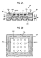
- FIGS.2A and 2B show a structure in which a semiconductor element is mounted on a wiring substrate 1A according to a first embodiment of the present invention.
- FIG.2A is a cross-sectional view of the wiring substrate 1A on which the semiconductor element is mounted
- FIG.2B is a plan view of the wiring substrate 1A.
- the wiring substrate 1A if classified roughly, is constructed by a wiring member 30 and a reinforcing layer 50.
- the wiring member 30 is formed by layering insulating layers 20, 20a, 20b, and wiring layers 18, 18a, 18b, 18c.
- the first wiring layers 18 serving as first connection terminals C1 are exposed from a surface 30a of the wiring member 30. Also, a solder resist 22 is formed on the back surface of the wiring member 30, and opening portions 22X are provided in the solder resist 22. Each of the fourth wiring layers 18c serving as a second connection terminal C2 is exposed from the opening portions 22X.
- the reinforcing layer 50 acts as a reinforcing member (stiffener) of the wiring member 30. As shown in FIG.2B , an opening portion 50X is formed in the center portion of the reinforcing layer 50, and surfaces of the first wiring layers 18 on the surface 30a of the wiring member 30 are exposed from the opening portion 50X.
- the reinforcing layer 50 is formed by etching a supporting body 10 ( see FIG.7D ). At this time, the opening portion 50X that exposes the surfaces of the first wiring layers 18 of the above wiring member 30 is also formed simultaneously.
- the reinforcing layer 50 has a plurality of concave-convex portions 50a.
- the concave-convex strip portion 50a according to the present embodiment is formed into an almost trapezoidal shape when viewed as a sectional profile. Because the plurality of concave-convex portions 50a is formed on the reinforcing layer 50, the reinforcing layer 50 comes down in weight. Also, because the concave-convex portions 50a are provided in light of a stiffness performance of the wiring member 30, in which a stress is concentrated and which is easily deformed, stiffness of the wiring member 30 can be effectively ensured.
- the sectional shape of the concave-convex strip portion is not limited to the above shape.
- a rectangular concave-convex portion 50b shown in FIG.3A a triangular concave-convex portion 50c shown in FIG.3B
- a U-shaped concave-convex portion 50d shown in FIG.3C a triangular concave-triangular convex portion 50e shown in FIG.3D
- a round wave concave-round wave convex portion 50f shown in FIG.3E may be employed as the sectional shape respectively.
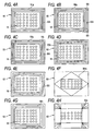
- a plurality of concave-convex portions 50a are formed like the square frame as the reinforcing layer 50 respectively.
- planar shape of the concave-convex portion 50a is not limited to the above shape.
- the planar shape may be constructed by concave-convex portions 50g extending in the horizontal direction (the first direction) in FIG.4A , and concave-convex portions 50h extending in the vertical direction (second direction) in FIG.4A .
- a concave-convex portions 50i extending in the right-upward direction (the third direction) in FIG.4B at a corner portion of the reinforcing layer 50 may be formed and also, as shown in FIG.4C , concave-convex portions 50j extending in the right-downward direction (the fourth direction) in FIG.4C at a corner portion of the reinforcing layer 50 may be formed.
- the concave-convex portions 50g and the concave-convex portions 50i may be connected with each other at the corner portion to be bent there and, as shown in FIG.4C , six concave-convex portions 50h and four concave-convex portions 50j may be connected in combination at the corner portion to withstand a stress concentration at the corner portion.
- concave-convex portions 50k formed like a square frame with slits may be constructed.
- concave-convex portions 501 formed like a polygonal frame may be constructed.
- concave-convex portions 50m obtained by turning quadrangular shapes by 1/4 turn may be constructed.
- concave-convex portions 50n whose corner portions are rounded may be constructed.
- concave-convex portions 50o formed to extend in the radial direction at the corner portion may be constructed.
- connection pads 18 are not limited to the structure shown in FIG.2 , and they can be set with a margin, as shown in FIGS.4A to 4H .
- a semiconductor chip 11 can be mounted on the side on which the solder resist 22 of the wiring member 30 is formed, and external connection terminals can be connected to the connection pads 18 on the side on which the semiconductor element mounting surface is provided (wiring substrate 1B).
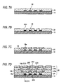
- FIGS.6 to 8 are cross-sectional views showing a method of manufacturing the wiring substrate 1A according to the first embodiment of the present invention.
- the supporting body 10 is prepared.
- a metal plate e.g., Cu
- a metallic foil may be used as the supporting body 10.
- a resist film 16 is formed on the supporting body 10 by using a dry film, for example.
- opening portions 16X are formed in predetermined portions (positions corresponding to forming positions of the connection pads 18 described later) by applying a patterning process to this resist film 16.
- the opening portions 16X may be formed in advance in the dry film-like resist film 16, and the resist film 16 having the opening portions 16X may be provided on the supporting body 10.
- connection pads 18 acting as the first wiring layers are formed on the supporting body 10 by the electroplating using the supporting body 10 as a plating power feeding layer.
- the connection pads 18 are formed in the opening portions 16X formed in the resist film 16.
- Each of the connection pads 18 includes a pad surface plating layer 25 and a pad main body 26.
- the pad surface plating layer 25 has a structure that is obtained by forming an Au film, a Pd film, and a Ni film sequentially. Therefore, upon forming the connection pad 18, firstly, the pad surface plating layer 25 is formed by plating an Au film, a Pd film, and a Ni film sequentially, and then the pad main body 26 made of Cu is formed on this pad surface plating layer 25 by the plating.
- connection pads 18 are formed. Then, as shown in FIG.6D , the resist film 16 is removed. In this case, the connection pads 18 function as the first connection terminals C1.
- the first insulating layer 20 for covering the connection pads 18 is formed on the supporting body 10.
- a resin material such as an epoxy resin or a polyimide resin may be used.
- a resin film is laminated on the supporting body 10, and then the resin film is cured by applying a heat treatment at a temperature of 130 to 150 °C while pressing the resin film, whereby the first insulating layer 20 can be obtained.
- first via holes 20X are formed by the laser beam machining such that the connection pads 18 are exposed from the first insulating layer 20 that is formed on the supporting body 10.
- the first insulating layer 20 may be formed by patterning a photosensitive resin film using photolithography technique, or may be formed by patterning the resin film having the openings using the screen printing technique.
- the second wiring layers 18a connected to the connection pads 18 (constituting the first wiring layers) formed on the supporting body 10 via the first via holes 20X are formed.
- the second wiring layers 18a may be formed of copper (Cu), and formed on the first insulating layer 20.
- the second wiring layers 18a are formed by the semi-additive process, for example.
- a Cu seed layer (not shown) is formed in the first via holes 20X and on the first insulating layer 20 by the electroless plating or the sputtering technique. Then, a resist film (not shown) having openings corresponding to the second wiring layers 18a is formed. Then, Cu layers patterns (not shown) are formed in the openings in the resist film respectively by the electroplating using the Cu seed layer as a plating power feeding layer.
- the resist film is removed.
- the second wiring layers 18a are formed by etching the Cu seed layer while using the Cu layer patterns as a mask.
- various wiring forming methods such as the subtractive process can be employed in addition to the above semi-additive process.
- the second insulating layer 20a for covering the second wiring layers 18a is formed on the supporting body 10 by repeatedly performing the similar steps, and then second via holes 20Y are formed in portions of the second insulating layer 20a on the second wiring layers 18a. Then, the third wiring layers 18b connected to the second wiring layers 18a via the second via holes 20Y are formed on the second insulating layer 20a of the supporting body 10.
- the third insulating layer 20b for covering the third wiring layers 18b is formed on the supporting body 10, and then third via hole 20Z are formed in portions of the third insulating layer 20b on the third wiring layers 18b. Then, the fourth wiring layers 18c connected to the third wiring layers 18b via the third via hole 20Z are formed on the third insulating layer 20b of the supporting body 10.
- the solder resist film 22 in which the opening portions 22X are provided is formed on the fourth wiring layers 18c of the supporting body 10. Accordingly, the fourth wiring layers 18c exposed from the opening portions 22X in the solder resist film 22 act as the second connection terminals C2.
- a desired build-up wiring layer is formed on the connection pads (the first connection terminals C1) on the supporting body 10.
- the four-layered build-up wiring layer (first to fourth wiring layers 18 to 18c) is formed.
- the n (n is an integral number in excess of 1)-layered build-up wiring layer may be formed.
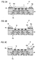
- a resist film 15 having patterns that correspond to the above concave-convex portions 50a is formed on the supporting body 10 acting as the supporting body.
- the etching is applied using the resist film 15 as a mask. According to this etching, the opening portion 50X is formed in the supporting body 10, and also the concave-convex portions 50a corresponding to the patterns in the resist 15 are formed on the supporting body remaining like the frame (referred to as the "reinforcing layer 50" hereinafter).
- the opening portion 50X and the concave-convex portions 50a may be formed at the same time by this etching process.
- the reinforcing layer 50 on which the concave-convex portions 50a are formed is formed by peeling off the resist.
- a process width L2 can be set to 30 ⁇ m ⁇ L2 ⁇ 500 ⁇ m.
- the stiffness can be enhanced by the reinforcing layer 50 having a plurality of concave-convex portions 50a, and the concave-convex portions 50a can be formed in the direction where the deformation of the wiring substrate can be withstood. As a result, the deformation can be prevented more effectively.
- FIG.9A is a cross-sectional view showing a wiring substrate 1C according to the second embodiment
- FIGS.9B and 9C show a variation of the wiring substrate 1C respectively.
- an adhesive member 60 is coated around the first wiring layers 18 of the wiring member 30, and then the reinforcing layer 50 having a plurality of concave-convex portions 50p is provided onto the adhesive member 60.
- a plurality of concave-convex portions 50p are formed in advance on a metal (copper, aluminum, or the like), a glass, a ceramic, a rigid resin, or a copper-clad laminate (whose FR grade is FR-4), for example, by the process apart from the steps of manufacturing the wiring member.
- the concave-convex portions 50p are formed by bending the plate member like crests and valleys.
- the shape of the concave-convex portions 50p of the reinforcing layer 50 may be constructed as shown in FIGS.4A to 4H , in addition to FIGS.3A to 3E . Further, as shown in FIG.9B , the concave-convex portions may be formed on the main body formed as a block. In FIG.9B , concave-convex portions 50q are provided on a wiring substrate 1D. As shown in FIG.9C , crest and valley shapes may be formed to face the surface of the wiring member 30, when viewed from a cross-sectional profile. In FIG.9C , concave-convex portions 50r are provided to face the surface of a wiring substrate 1E.
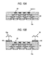
- FIGS.10A and 10B are views showing a method of manufacturing the wiring substrate 1C according to the second embodiment.
- the same reference symbols are affixed to the configurations corresponding to the configurations shown in FIGS.6A to 7D , and their description will be omitted herein.
- the wiring member 30 is formed on the supporting body 10 by the same manufacturing method as that of the wiring substrate 1A according to the first embodiment of the present invention and the steps are the same as those shown in FIG.6A to 7D .
- the supporting body 10 acting as the supporting body is removed.
- the supporting body 10 may be removed by the wet etching using an iron (III) chloride aqueous solution, a copper (II) chloride aqueous solution, an ammonium peroxodisulfate aqueous solution, or the like.
- thermosetting adhesive 60 is used in the bonding process.
- the thermosetting adhesive 60 is not limited to the thermosetting type adhesive, and various adhesives such as an ultraviolet curable type adhesive may be employed.
- the reinforcing layer 50 of the wiring substrate 1C according to the present embodiment can be formed through the manufacturing steps that are performed separately from the manufacturing steps of the wiring member 30.
- the reinforcing layer 50 having the concave-convex portions 50p can be obtained by applying the press working to the metal plate.
- the reinforcing layer 50 of the wiring substrate 1C formed through the above processes can be reduced in weight as compared with the related art, and further the stiffness (shape stiffness) of the reinforcing layer 50 can be enhanced.
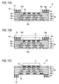
- FIG.11A is a cross-sectional view of the wiring substrate 1F
- FIG.11B is a cross-sectional view of the wiring substrate 1F on which a semiconductor element and a heat spreader (indicated with a broken line in FIG.11B ) are mounted.
- the wiring substrate 1F is constructed by the wiring member 30 and the reinforcing layer 50.
- the wiring member 30 is formed by layering the insulating layers 20 to 20b and the wiring layers 18 to 18c, and the connection pads 18 are exposed from the surface 30a of the wiring member 30.
- the solder resist 22 having the opening portions 22X is formed on the back surface of the wiring member 30, and the fourth wiring layer 18c is exposed from the opening portions 22X.
- the opening portion 50X is formed in the reinforcing layer 50, and the connection pads 18 on the wiring member 30 are exposed from the opening portion 50X.
- the reinforcing layer 50 has a plurality of concave-convex portions 50s.
- a nickel layer 19 is provided on convex top end portions 55 of the concave-convex portions 50s respectively.
- the nickel layer 19 is provided on the concave-convex portions 50s of the reinforcing layer 50 formed of copper. Therefore, the stiffness of the reinforcing layer 50 can be further improved because a stiffness of the nickel is higher than the copper.
- FIG.11B is a view showing a state that a heat spreader 80 connected thermally to the semiconductor element 11 is provided on the reinforcing layer 50.
- the heat spreader 80 should be adhered to the back surface of the semiconductor element 11 by an adhesive or a solder.
- the reinforcing layer 50 can achieve such an advantage that the heat spreader 80 is not press-contacted to the semiconductor element 11.
- adhesion of the nickel to the adhesive or the solder is higher than the copper. Therefore, since the nickel layer 19 is provided to the convex top end portions 55 respectively, the heat spreader 80 can be adhered more strongly onto the concave-convex portions 50s.
- the concave-convex portions 50s according to the present embodiment are constructed to have an almost trapezoidal shape when viewed from a cross-sectional profile.
- the concave-convex portions 50s may be constructed like FIGS.4A to 4H in addition to above FIGS.3A to 3E .
- a wiring substrate 1G shown in FIG.11C is constructed such that, in the above wiring substrate 1F, the semiconductor chip 11 is mounted on the side on which the solder resist 22 of the wiring member 30 is formed, and the external connection terminals are connected to the connection pads 18 in the semiconductor element mounting surface side. In this configuration, the similar advantages to the above wiring substrate 1F can also be achieved.
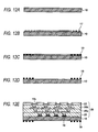
- FIGS.12A to 12E are cross-sectional views showing the method of manufacturing the wiring substrate 1F according to the third embodiment.
- the same reference symbols are affixed to the configuration corresponding to the configuration shown in FIG. 6A to 7D , and their description will be omitted herein.
- the same supporting body 10 as that used in the first embodiment is prepared.
- a resist film 17 having the patterns corresponding to the concave-convex portions 50s is formed on the supporting body 10, and then patterning process is performed.
- a nickel is plated while using the supporting body 10 as a power feeding layer.
- the nickel layer 19 serving as a mask that is used to form the opening portion 50X and the concave-convex portions 50s is formed on the supporting body 10 by removing the plating resist 17.
- the wiring member 30 is formed on a back surface opposite to the surface of the supporting body 10 on which the nickel layer 19 is formed, by the manufacturing steps similar to those in the first embodiment shown in FIGS.6A to 7D ( see FIG.12E ).
- a plurality of concave-convex portions 50s and the reinforcing layer 50 are formed in the steps shown in FIGS.8A and 8B .
- the resist film 15 used to etch the supporting body 10 is formed on the supporting body 10 shown in FIG.8A .
- the nickel layer 19 has already been formed in the first stage shown in FIG.12 . Therefore, in the present embodiment, the supporting body 10 is etched using the nickel layer 19 in FIG.8B as a mask. As a result, the opening portion 50X in the reinforcing layer 50 can be formed while the reinforcing layer 50 having the concave-convex portions 50s is formed.
Landscapes
- Engineering & Computer Science (AREA)
- Microelectronics & Electronic Packaging (AREA)
- Manufacturing & Machinery (AREA)
- Structure Of Printed Boards (AREA)
- Production Of Multi-Layered Print Wiring Board (AREA)
Applications Claiming Priority (1)
| Application Number | Priority Date | Filing Date | Title |
|---|---|---|---|
| JP2007302007A JP2009130054A (ja) | 2007-11-21 | 2007-11-21 | 配線基板及びその製造方法 |
Publications (2)
| Publication Number | Publication Date |
|---|---|
| EP2066156A2 true EP2066156A2 (fr) | 2009-06-03 |
| EP2066156A3 EP2066156A3 (fr) | 2009-12-02 |
Family
ID=40409951
Family Applications (1)
| Application Number | Title | Priority Date | Filing Date |
|---|---|---|---|
| EP08169709A Withdrawn EP2066156A3 (fr) | 2007-11-21 | 2008-11-21 | Substrat de câblage et son procédé de fabrication |
Country Status (5)
| Country | Link |
|---|---|
| US (1) | US20090134530A1 (fr) |
| EP (1) | EP2066156A3 (fr) |
| JP (1) | JP2009130054A (fr) |
| KR (1) | KR20090052814A (fr) |
| TW (1) | TW200924596A (fr) |
Families Citing this family (8)
| Publication number | Priority date | Publication date | Assignee | Title |
|---|---|---|---|---|
| JP5120342B2 (ja) * | 2009-06-18 | 2013-01-16 | ソニー株式会社 | 半導体パッケージの製造方法 |
| US8127979B1 (en) * | 2010-09-25 | 2012-03-06 | Intel Corporation | Electrolytic depositon and via filling in coreless substrate processing |
| KR102079256B1 (ko) | 2013-09-13 | 2020-02-20 | 삼성디스플레이 주식회사 | 표시장치 및 이의 제조방법 |
| JP2017017238A (ja) * | 2015-07-03 | 2017-01-19 | 株式会社ジェイデバイス | 半導体装置及びその製造方法 |
| US20180190596A1 (en) * | 2016-12-30 | 2018-07-05 | Intel Corporation | Standoff members for semiconductor package |
| KR101938104B1 (ko) * | 2018-01-25 | 2019-01-14 | 주식회사 기가레인 | 접합 평탄도가 개선된 연성회로기판 |
| CN112038242A (zh) * | 2020-09-10 | 2020-12-04 | 华进半导体封装先导技术研发中心有限公司 | 先重布线扇出型封装方法及结构 |
| KR102901072B1 (ko) * | 2023-08-07 | 2025-12-16 | 삼성전기주식회사 | 회로 기판 |
Citations (1)
| Publication number | Priority date | Publication date | Assignee | Title |
|---|---|---|---|---|
| WO2003039219A1 (fr) | 2001-10-31 | 2003-05-08 | Shinko Electric Industries Co., Ltd. | Procede de fabrication de carte de circuits imprimes multicouches pour dispositif a semiconducteur |
Family Cites Families (10)
| Publication number | Priority date | Publication date | Assignee | Title |
|---|---|---|---|---|
| JPH1050877A (ja) * | 1996-07-30 | 1998-02-20 | Toshiba Corp | 半導体パッケージ |
| JP4400802B2 (ja) * | 1999-08-23 | 2010-01-20 | 大日本印刷株式会社 | リードフレーム及びその製造方法並びに半導体装置 |
| JP2002299495A (ja) * | 2001-03-30 | 2002-10-11 | Fuji Electric Co Ltd | 半導体回路基板 |
| US6552267B2 (en) * | 2001-08-13 | 2003-04-22 | Taiwan Semiconductor Manufacturing Co., Ltd. | Microelectronic assembly with stiffening member |
| SG102637A1 (en) * | 2001-09-10 | 2004-03-26 | Micron Technology Inc | Bow control in an electronic package |
| JP3615727B2 (ja) * | 2001-10-31 | 2005-02-02 | 新光電気工業株式会社 | 半導体装置用パッケージ |
| JP4094494B2 (ja) * | 2002-08-23 | 2008-06-04 | 新光電気工業株式会社 | 半導体パッケージ |
| WO2004086498A1 (fr) * | 2003-03-26 | 2004-10-07 | Fujitsu Limited | Dispositif a semi-conducteur |
| JP4460341B2 (ja) * | 2004-04-09 | 2010-05-12 | 日本特殊陶業株式会社 | 配線基板およびその製造方法 |
| JP2006186136A (ja) * | 2004-12-28 | 2006-07-13 | Toshiba Corp | 両面部品実装回路基板及びその製造方法 |
-
2007
- 2007-11-21 JP JP2007302007A patent/JP2009130054A/ja active Pending
-
2008
- 2008-11-20 US US12/274,719 patent/US20090134530A1/en not_active Abandoned
- 2008-11-20 KR KR1020080115571A patent/KR20090052814A/ko not_active Withdrawn
- 2008-11-21 EP EP08169709A patent/EP2066156A3/fr not_active Withdrawn
- 2008-11-21 TW TW097145075A patent/TW200924596A/zh unknown
Patent Citations (1)
| Publication number | Priority date | Publication date | Assignee | Title |
|---|---|---|---|---|
| WO2003039219A1 (fr) | 2001-10-31 | 2003-05-08 | Shinko Electric Industries Co., Ltd. | Procede de fabrication de carte de circuits imprimes multicouches pour dispositif a semiconducteur |
Also Published As
| Publication number | Publication date |
|---|---|
| TW200924596A (en) | 2009-06-01 |
| JP2009130054A (ja) | 2009-06-11 |
| US20090134530A1 (en) | 2009-05-28 |
| KR20090052814A (ko) | 2009-05-26 |
| EP2066156A3 (fr) | 2009-12-02 |
Similar Documents
| Publication | Publication Date | Title |
|---|---|---|
| EP2066157A2 (fr) | Substrat de câblage et son procédé de fabrication | |
| EP2066156A2 (fr) | Substrat de câblage et son procédé de fabrication | |
| KR101156751B1 (ko) | 리지드 플렉서블 프린트 배선판 및 리지드 플렉서블 프린트배선판의 제조방법 | |
| US9060459B2 (en) | Printed wiring board and method for manufacturing same | |
| KR101093594B1 (ko) | 회로 기판의 제조 방법 | |
| US6969436B2 (en) | Method and structure for producing Z-axis interconnection assembly of printed wiring board elements | |
| US9215812B2 (en) | Support body, method of manufacturing support body, method of manufacturing wiring board, method of manufacturing electronic component, and wiring structure | |
| CN103404243B (zh) | 印刷电路板及其制造方法 | |
| KR20090056824A (ko) | 배선 기판 및 전자 부품 장치 | |
| JP5025399B2 (ja) | 配線基板及びその製造方法 | |
| KR100619348B1 (ko) | 무전해 니켈 도금을 이용한 패키지 기판의 제조 방법 | |
| US10219369B2 (en) | Circuit board | |
| EP1827067B1 (fr) | Procédé de production d'un substrat à circuit | |
| JP2007110010A (ja) | フレキシブルプリント配線板、フレキシブルプリント回路板、およびそれらの製造方法 | |
| JP2018195600A (ja) | 配線基板、配線基板の製造方法 | |
| JPH07193370A (ja) | フレックスリジッドプリント基板及びその製造方法 | |
| JP2008159973A (ja) | 電子部品モジュールおよびこれを内蔵した部品内蔵回路基板 | |
| JPH0799391A (ja) | 電子部品搭載用多層基板の製造方法 | |
| KR20190069164A (ko) | 양면 임베디드 회로를 갖는 인쇄회로기판 및 그 제조 방법 | |
| JP2007013048A (ja) | 多層配線基板の製造方法 | |
| KR100693146B1 (ko) | 다층 인쇄회로기판의 제조방법 | |
| KR20030022703A (ko) | 전자부품 실장용기판 및 전자부품 실장용기판의 휨 제거방법 | |
| KR101231343B1 (ko) | 인쇄회로기판 및 그의 제조 방법 | |
| JP4926676B2 (ja) | 多層プリント配線板の製造方法 | |
| JP2018182252A (ja) | プリント配線板の製造方法 |
Legal Events
| Date | Code | Title | Description |
|---|---|---|---|
| PUAI | Public reference made under article 153(3) epc to a published international application that has entered the european phase |
Free format text: ORIGINAL CODE: 0009012 |
|
| AK | Designated contracting states |
Kind code of ref document: A2 Designated state(s): AT BE BG CH CY CZ DE DK EE ES FI FR GB GR HR HU IE IS IT LI LT LU LV MC MT NL NO PL PT RO SE SI SK TR |
|
| AX | Request for extension of the european patent |
Extension state: AL BA MK RS |
|
| PUAL | Search report despatched |
Free format text: ORIGINAL CODE: 0009013 |
|
| AK | Designated contracting states |
Kind code of ref document: A3 Designated state(s): AT BE BG CH CY CZ DE DK EE ES FI FR GB GR HR HU IE IS IT LI LT LU LV MC MT NL NO PL PT RO SE SI SK TR |
|
| AX | Request for extension of the european patent |
Extension state: AL BA MK RS |
|
| 17P | Request for examination filed |
Effective date: 20100121 |
|
| AKX | Designation fees paid |
Designated state(s): DE |
|
| STAA | Information on the status of an ep patent application or granted ep patent |
Free format text: STATUS: THE APPLICATION IS DEEMED TO BE WITHDRAWN |
|
| 18D | Application deemed to be withdrawn |
Effective date: 20120601 |