EP2073383A1 - Verstärkeranordnung - Google Patents
Verstärkeranordnung Download PDFInfo
- Publication number
- EP2073383A1 EP2073383A1 EP07254963A EP07254963A EP2073383A1 EP 2073383 A1 EP2073383 A1 EP 2073383A1 EP 07254963 A EP07254963 A EP 07254963A EP 07254963 A EP07254963 A EP 07254963A EP 2073383 A1 EP2073383 A1 EP 2073383A1
- Authority
- EP
- European Patent Office
- Prior art keywords
- gain
- amplifier
- signal
- input
- controlled
- Prior art date
- Legal status (The legal status is an assumption and is not a legal conclusion. Google has not performed a legal analysis and makes no representation as to the accuracy of the status listed.)
- Granted
Links
- 238000000034 method Methods 0.000 claims description 23
- 238000006243 chemical reaction Methods 0.000 claims description 4
- 230000008569 process Effects 0.000 description 7
- 230000000694 effects Effects 0.000 description 6
- 239000003990 capacitor Substances 0.000 description 5
- 239000013256 coordination polymer Substances 0.000 description 4
- 230000008859 change Effects 0.000 description 3
- 238000012935 Averaging Methods 0.000 description 2
- 230000003321 amplification Effects 0.000 description 2
- 230000001276 controlling effect Effects 0.000 description 2
- 238000010586 diagram Methods 0.000 description 2
- 238000002408 directed self-assembly Methods 0.000 description 2
- 238000003199 nucleic acid amplification method Methods 0.000 description 2
- 240000007320 Pinus strobus Species 0.000 description 1
- XUIMIQQOPSSXEZ-UHFFFAOYSA-N Silicon Chemical compound [Si] XUIMIQQOPSSXEZ-UHFFFAOYSA-N 0.000 description 1
- 230000002238 attenuated effect Effects 0.000 description 1
- 230000001419 dependent effect Effects 0.000 description 1
- 230000007246 mechanism Effects 0.000 description 1
- 230000001105 regulatory effect Effects 0.000 description 1
- 230000004044 response Effects 0.000 description 1
- 229910052710 silicon Inorganic materials 0.000 description 1
- 239000010703 silicon Substances 0.000 description 1
Images

Classifications
-
- H—ELECTRICITY
- H03—ELECTRONIC CIRCUITRY
- H03G—CONTROL OF AMPLIFICATION
- H03G3/00—Gain control in amplifiers or frequency changers
- H03G3/20—Automatic control
- H03G3/30—Automatic control in amplifiers having semiconductor devices
- H03G3/3036—Automatic control in amplifiers having semiconductor devices in high-frequency amplifiers or in frequency-changers
- H03G3/3042—Automatic control in amplifiers having semiconductor devices in high-frequency amplifiers or in frequency-changers in modulators, frequency-changers, transmitters or power amplifiers
-
- H—ELECTRICITY
- H03—ELECTRONIC CIRCUITRY
- H03G—CONTROL OF AMPLIFICATION
- H03G3/00—Gain control in amplifiers or frequency changers
- H03G3/001—Digital control of analog signals
Definitions
- the present invention relates generally to amplifiers, and more specifically but not exclusively to method of controlling the gain of an RF amplifier device and to a gain-controlled RF amplifier system.
- the gain control of an open-loop amplifier is usually done by varying one or more of the gain parameters e.g. Gm (transconductance of the transistor), magnitude of source or load impedance etc, thus achieving a range of gain values.
- Gm transmission of the transistor
- Amplifier circuits realized using physical devices available in an integrated circuit process are subject to uncontrollable statistical variations in process, supply voltage and temperature (PVT). Therefore amplifier gain can drift from the desired gain value due to PVT variations.
- This problem may be alleviated in DC and low-frequency amplifiers by employing the technique of negative feedback; here open-loop gain of the amplifier is traded off to reduce the effects of PVT variations.
- US-A-5768694 discloses an AGC circuit used in radio transmitters for satellite communications and the like intended to eliminate non-linearity compensators for detectors and reduce the radio transmitters in size and complexity.
- An RF input signal is amplified and output while passing through input splitting means, programmable attenuator, amplifier, and output splitting means.
- a part of the RF input signal branches off at the input splitting means to input detecting means, where it is detected so as to obtain an input signal amplitude.
- a part of the amplifier output is split off at the output splitting means, then attenuated by attenuation means and finally reaches output detecting means, where the signal is detected so as to obtain an output signal amplitude after attenuation.
- Control means adjusts the attenuation factor of the programmable attenuator so that the input of the input detecting means will be equal to the input of the output detecting means.
- US-A-7065155 discloses a transceiver and a method of operating the same that includes in the transmitter a power control circuit that operates on an analog differential signal containing data packets individually.
- the power control circuit initially transmits a series of data symbols with known values, periodically strobes the transceiver system for correct power levels and incrementally increases the power level of the transceiver until the optimal gain is reached, without exceeding the maximum output power.
- a method of controlling the gain of an RF amplifier device having an input signal and an output signal comprising comparing a measure of magnitude of the input signal to a like measure of magnitude of the output signal; and using a result of the comparison to selectively enable amplifiers making up said amplifier device.
- the input signal may be at a first frequency, and the output signal at a second frequency different to the first frequency.
- the first frequency may be higher than the second.
- the first frequency is lower than the second.
- the first and second frequencies are the same as one another.
- the method may further comprise using a result of the comparison to control a gain of at least one enabled amplifier.
- the method may further comprise scaling at least one of the input signal and the output signal.
- the step of using the comparison result may comprise of applying the comparison result to a digital state machine to derive digital control signals for enabling respective amplifiers.
- the digital state machine may be used with logic to derive the control signals; alternatively logic alone may be used.
- a gain-controlled RF amplifier system having an input node and an output node, comprising a plurality of amplifier devices, selectively connectable between the input node and the output node; means for comparing a magnitude of a signal input to the input node against a magnitude of a signal output from the output node; control means responsive to the comparison result to select between the plurality of amplifier devices.
- control means may be responsive to the comparison result to vary the gain of at least one amplifier device
- the amplifier devices may be generally in parallel.
- At least one amplifier device may be in series with another amplifier device.
- the gain-controlled RF amplifier system may have a digital state machine configured to receive the comparison result, thereby to provide digital control signals to control respective amplifier devices
- the digital state machine may be used with logic; alternatively logic alone may be used in some embodiments,
- At least one controllable scaling device may provide the or each input to a magnitude comparator.
- At least one signal detector may be used in determining what signals are to be compared.
- a signal detector may be an envelope detector, a peak value circuit, RMS measuring circuit, averaging circuit or other detector, as appropriate.
- gain control is exercised by switching ON or OFF discrete gain stages. These may be, for example, binary weighted or dB weighted gain stages, and may be connected in parallel.
- a digital control signal may be generated by successive approximation using a comparator that compares the 'equalized', detected input and output signals.
- Embodiments allow gain control without change of biasing conditions of the gain stages.
- gain is controlled by the number of individual gain stages switched ON at the time. Consequently, the gain control range is only limited by the number of individual gain stages connected in parallel.
- the digital gain control technique is digital in operation and thus can be readily read, written to and stored for further computation by means of hardware or software control e.g. baseband chip in wireless communication transceiver.
- Embodiments of the invention enable a technique of RF amplification whereby gain can be precisely controlled and/or made independent of process, supply voltage and temperature variations automatically.
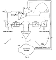
- a first envelope detector ED1 is connected between the first tap node 3 and a first input node 5 of a comparator CP.
- a second envelope detector ED2 - is connected between the second tap node 4 and a second input node 6 of the comparator CP.
- the comparator CP has an output node 7, which is connected to a digital state machine DSM.
- the digital state machine is connected to the respective gain stages A 1 -An via plural control lines 11.
- a first set of control signals C1 is provided by the digital state machine to switch respective gain stages into and out of circuit.
- detector devices rather than envelope detectors.
- peak detectors or RMS measuring devices or averaging circuits may be used, where appropriate to the desired effect.
- the position of the tap point on each tapped attenuator, and hence the proportion of the respective input signal supplied to the respective tap point, of this embodiment is controllable by a digital gain control signal CS.
- each gain stage is not only switchable by the first control signal C1, but also has a variable gain that is controlled by another digital control signal C2.
- the overall gain of the amplifier system is digitally programmable over user-defined range by means of control signals C1 and C2.
- the actual gain G a of the amplifier system is defined as the ratio of the RF signal at node 2 to that at node 1. Further it is equal to the summation of gain values of all N individual stages, each of which is dependent on the state of respective digital control signals [C1, C2].
- G a S 2
- G d The desired gain setting of the amplifier system is denoted as G d which is a set of user-defined values spanning a range from G d,low to G d,high with discrete unit step ⁇ Gd .
- the resolution of the amplifier gain discrete step is designed to be greater than the resolution of discrete unit step of the desired gain values.
- An automatic gain control scheme regulates the actual gain G a of the amplifier system, to keep it equal to the desired gain setting of the amplifier, G d , in response to any intended change in G d such as setting a different gain value or unintended deviation, for instance due to process, supply voltage or temperature variations.
- the AGC scheme functions as follows:
- Digital Step Attenuators DSA1 and DSA2 have high input impedance; therefore, their loading on the signal path circuitry of the amplifier is insignificant and does not affect the actual information in the signal.
- the function of DSA1 and DSA2 is to attenuate the sensed signal linearly in relation to the desired gain setting, G d , of the amplifier system.
- the DSA attenuation value is based on the ratio of the values of passive devices available in an IC process (e.g. resistors or capacitors).
- the resistors or capacitors in a modem IC process can be manufactured to precise values and their PVT variations can be matched to a high degree of accuracy. Therefore, an attenuation value based on ratio of values of resistors or capacitors is highly accurate even in presence of PVT variations.
- DSA1's set of discrete attenuation values AT 1 is equal to the subset of G d whose values are ⁇ 1 in magnitude or equivalently ⁇ 0 in dB terms.
- DSA2's set of discrete attenuation values AT 2 is equal to the subset of G d whose values are >1 in magnitude or equivalently >0 in dB terms.
- a ⁇ T 1 ⁇ G d
- DSAs are implemented as digitally programmable resistor ladder attenuators with discrete set of attenuation values as defined above.
- Other alternatives for example capacitors are possible.
- Nodes 3 and 4 are coupled to the input of envelope detectors ED1 and ED2 respectively.
- ED 1 and ED2 convert the RF signals S3 and S4 to equivalent quasi-dc signals S5 and S6 available at the output of envelope detectors at nodes 5 and 6 respectively.
- Nodes 5 and 6 are coupled to the input of a comparator labeled CP.
- the comparator senses the difference in signals S5 and S6 and outputs a binary digital signal S7 at node 7 based on the polarity of the difference between signals S5 and S6.
- the digital signal S7 is coupled to a Digital State Machine labeled DSM which is implemented as a logic computation circuit.
- DSM computes a digital control signal [C1, C2] that is fed back to the amplifier to control its gain.
- the digital control signal [C1, C2] acts in opposite to the sense of difference in S3 and S4, thus giving a negative feedback signal to the amplifier.
- G a to be greater than G d .
- S4(S6) would be greater than S3(S5).
- the comparator outputs a binary digital signal S7 to indicate this condition to DSM which in turn produces digital control signal [C1, C2] to reduce the gain of the amplifier.
- the AGC Loop automatically controls the RF amplifier gain to equal to the digitally programmable desired gain setting and in the process eliminating effects of any PVT variations.
- the gain stages are constant in gain, and are merely switched into and out of circuit to provide gain control.
- at least one gain stage is not switchable and is always in circuit.
- at least one gain stage is in series with another gain stage. In that case a "disabled" gain stage may have unity gain when in the disabled state.
- a frequency down conversion block herein referred to as 'Mixer' connected between node1 and input of the amplifier or similarly between output of the amplifier and node 2.
- 'Mixer' a frequency down conversion block connected between node1 and input of the amplifier or similarly between output of the amplifier and node 2.
- the frequency f1 of input signal S 1 may be different from the frequency f2 of output signal S2.
- the mixer may alternatively be used for up-conversion in a further embodiment.
- the mixer may have a gain or loss value of its own.
- This embodiment illustrates the gain control mechanism of the combined amplifier and mixer such that the combined gain is regulated to a user-specified gain setting and gain variations due to PVT effects are eliminated.
Landscapes
- Control Of Amplification And Gain Control (AREA)
Priority Applications (2)
| Application Number | Priority Date | Filing Date | Title |
|---|---|---|---|
| EP07254963A EP2073383B1 (de) | 2007-12-19 | 2007-12-19 | Verstärkeranordnung |
| US12/338,702 US7994855B2 (en) | 2007-12-19 | 2008-12-18 | Amplifier arrangement |
Applications Claiming Priority (1)
| Application Number | Priority Date | Filing Date | Title |
|---|---|---|---|
| EP07254963A EP2073383B1 (de) | 2007-12-19 | 2007-12-19 | Verstärkeranordnung |
Publications (2)
| Publication Number | Publication Date |
|---|---|
| EP2073383A1 true EP2073383A1 (de) | 2009-06-24 |
| EP2073383B1 EP2073383B1 (de) | 2011-08-10 |
Family
ID=39295511
Family Applications (1)
| Application Number | Title | Priority Date | Filing Date |
|---|---|---|---|
| EP07254963A Not-in-force EP2073383B1 (de) | 2007-12-19 | 2007-12-19 | Verstärkeranordnung |
Country Status (2)
| Country | Link |
|---|---|
| US (1) | US7994855B2 (de) |
| EP (1) | EP2073383B1 (de) |
Cited By (1)
| Publication number | Priority date | Publication date | Assignee | Title |
|---|---|---|---|---|
| EP4182708A2 (de) * | 2020-07-17 | 2023-05-24 | Qualcomm Incorporated | Leistungsdetektor |
Families Citing this family (2)
| Publication number | Priority date | Publication date | Assignee | Title |
|---|---|---|---|---|
| CN107104646B (zh) * | 2010-04-23 | 2021-07-16 | 苹果公司 | 信号放大电路及信号放大方法 |
| US9379675B2 (en) * | 2014-02-20 | 2016-06-28 | Analog Devices Global | Power detector with overdrive detection |
Citations (10)
| Publication number | Priority date | Publication date | Assignee | Title |
|---|---|---|---|---|
| GB2161335A (en) | 1984-07-06 | 1986-01-08 | Int Standard Electric Corp | Variable gain power amplifier |
| GB2161336A (en) | 1984-05-22 | 1986-01-08 | Casio Computer Co Ltd | Television video signal a/d converter |
| EP0424009A2 (de) | 1989-10-18 | 1991-04-24 | Nokia Mobile Phones Ltd. | Automatische Verstärkungsregelungsschaltung für Funktelefonempfänger |
| EP0472399A2 (de) | 1990-08-20 | 1992-02-26 | Mitsui Petrochemical Industries, Ltd. | HLA-DR Antigen-Gen, dessen Nukleotidsequenz und Verwendung |
| EP0473299A2 (de) | 1990-08-30 | 1992-03-04 | Hughes Aircraft Company | Festkörperleistungsverstärker mit dynamisch verstellbarem Arbeitspunkt |
| EP0701332A1 (de) | 1994-09-09 | 1996-03-13 | Kabushiki Kaisha Toshiba | Schaltung für variable Verstärkung und Radioapparat mit eines solche Schatung |
| US6091942A (en) | 1996-12-02 | 2000-07-18 | Motorola, Inc. | Self gain aligning circuit and method |
| WO2001011769A1 (en) | 1999-08-04 | 2001-02-15 | Harris Corporation | Methods for calibration of radio devices at room temperature |
| EP1083668A1 (de) | 1999-02-25 | 2001-03-14 | Mitsubishi Denki Kabushiki Kaisha | Funkendgerät |
| US7065155B2 (en) | 2000-12-22 | 2006-06-20 | Atheros Communications, Inc. | Method and apparatus for a transceiver having a constant power output |
Family Cites Families (8)
| Publication number | Priority date | Publication date | Assignee | Title |
|---|---|---|---|---|
| JPH08265073A (ja) * | 1995-03-20 | 1996-10-11 | Fujitsu Ltd | Agc回路 |
| JP3094955B2 (ja) * | 1997-06-23 | 2000-10-03 | 日本電気株式会社 | 送信増幅器制御回路 |
| JPH11136154A (ja) * | 1997-10-31 | 1999-05-21 | Sony Corp | 受信装置 |
| US6124758A (en) * | 1998-08-19 | 2000-09-26 | Harris Corporation | RF power amplifier control system |
| US6812466B2 (en) * | 2002-09-25 | 2004-11-02 | Prospects, Corp. | Infrared obstacle detection in the presence of sunlight |
| JP4652130B2 (ja) * | 2004-06-04 | 2011-03-16 | パナソニック株式会社 | 多段増幅装置、並びにそれを用いた受信回路及び送信回路 |
| KR100957417B1 (ko) * | 2004-12-08 | 2010-05-11 | 삼성전자주식회사 | 무선 통신 시스템에서 스위칭 구조를 이용한 전력 증폭 장치 및 제어 방법 |
| US7859336B2 (en) * | 2007-03-13 | 2010-12-28 | Astec International Limited | Power supply providing ultrafast modulation of output voltage |
-
2007
- 2007-12-19 EP EP07254963A patent/EP2073383B1/de not_active Not-in-force
-
2008
- 2008-12-18 US US12/338,702 patent/US7994855B2/en not_active Expired - Fee Related
Patent Citations (10)
| Publication number | Priority date | Publication date | Assignee | Title |
|---|---|---|---|---|
| GB2161336A (en) | 1984-05-22 | 1986-01-08 | Casio Computer Co Ltd | Television video signal a/d converter |
| GB2161335A (en) | 1984-07-06 | 1986-01-08 | Int Standard Electric Corp | Variable gain power amplifier |
| EP0424009A2 (de) | 1989-10-18 | 1991-04-24 | Nokia Mobile Phones Ltd. | Automatische Verstärkungsregelungsschaltung für Funktelefonempfänger |
| EP0472399A2 (de) | 1990-08-20 | 1992-02-26 | Mitsui Petrochemical Industries, Ltd. | HLA-DR Antigen-Gen, dessen Nukleotidsequenz und Verwendung |
| EP0473299A2 (de) | 1990-08-30 | 1992-03-04 | Hughes Aircraft Company | Festkörperleistungsverstärker mit dynamisch verstellbarem Arbeitspunkt |
| EP0701332A1 (de) | 1994-09-09 | 1996-03-13 | Kabushiki Kaisha Toshiba | Schaltung für variable Verstärkung und Radioapparat mit eines solche Schatung |
| US6091942A (en) | 1996-12-02 | 2000-07-18 | Motorola, Inc. | Self gain aligning circuit and method |
| EP1083668A1 (de) | 1999-02-25 | 2001-03-14 | Mitsubishi Denki Kabushiki Kaisha | Funkendgerät |
| WO2001011769A1 (en) | 1999-08-04 | 2001-02-15 | Harris Corporation | Methods for calibration of radio devices at room temperature |
| US7065155B2 (en) | 2000-12-22 | 2006-06-20 | Atheros Communications, Inc. | Method and apparatus for a transceiver having a constant power output |
Cited By (1)
| Publication number | Priority date | Publication date | Assignee | Title |
|---|---|---|---|---|
| EP4182708A2 (de) * | 2020-07-17 | 2023-05-24 | Qualcomm Incorporated | Leistungsdetektor |
Also Published As
| Publication number | Publication date |
|---|---|
| EP2073383B1 (de) | 2011-08-10 |
| US20090160554A1 (en) | 2009-06-25 |
| US7994855B2 (en) | 2011-08-09 |
Similar Documents
| Publication | Publication Date | Title |
|---|---|---|
| CA2093844C (en) | Power detection technique for automatic amplifier power control | |
| US9748912B2 (en) | Method and apparatus for detecting power | |
| CN101688889B (zh) | 带波峰因数测量的rf检测器 | |
| EP0509733A2 (de) | Leistungsverstärker für Hochfrequenzsignale | |
| US5095542A (en) | Apparatus for controlling transmission output level for burst signal | |
| EP0720287A2 (de) | Leistungsverstärker mit grosser Dynamik | |
| US4754231A (en) | Automatic control circuitry for a signal power amplifier | |
| WO2007121112A2 (en) | Systems, methods and devices for dual closed loop modulation controller for nonlinear rf amplifier | |
| US10033364B1 (en) | Low power compact peak detector with improved accuracy | |
| EP1400013B1 (de) | Verfahren und vorrichtung für einen sender/empfänger mit konstanter ausgangsleistung | |
| EP3729108B1 (de) | Leistungsdetektor für hochfrequenzleistungsverstärkerschaltungen | |
| US6999012B2 (en) | Temperature compensation device for automatic gain control loop | |
| EP2073383A1 (de) | Verstärkeranordnung | |
| US5963087A (en) | Gain control circuit and method for providing gain control of a variable amplifier using a pilot signal | |
| US20070109055A1 (en) | Soft saturation detection for power amplifiers | |
| EP1478104A1 (de) | Variable Schrittgrösse der Sendeleistung | |
| US6091299A (en) | Method and apparatus for achieving linearized response of PIN diode attenuators | |
| WO2007016967A1 (en) | Loop gain equalizer for rf power amplifier | |
| CA2743484C (en) | Hybrid power control for a power amplifier | |
| KR19990002976U (ko) | 자동 레벨 조정장치 | |
| JPH02217011A (ja) | 送信装置の送信電力制御回路 | |
| EP1932234A2 (de) | System und verfahren zur steigerung der genauigkeit der feststellung der sendeleistung über einen grösseren bereich von sendeleistungsstufen | |
| KR100415524B1 (ko) | 파일롯 신호를 사용하여 가변 증폭기의 이득 제어를제공하기 위한 이득 제어 회로 및 방법 | |
| JP3064981B2 (ja) | 送信電力自動制御回路 | |
| EP1137173A1 (de) | HF-Fet Vorspannungs- und Schaltvorrichtung basierend auf einer quasi offenen Regelschleife |
Legal Events
| Date | Code | Title | Description |
|---|---|---|---|
| PUAI | Public reference made under article 153(3) epc to a published international application that has entered the european phase |
Free format text: ORIGINAL CODE: 0009012 |
|
| AK | Designated contracting states |
Kind code of ref document: A1 Designated state(s): AT BE BG CH CY CZ DE DK EE ES FI FR GB GR HU IE IS IT LI LT LU LV MC MT NL PL PT RO SE SI SK TR |
|
| AX | Request for extension of the european patent |
Extension state: AL BA HR MK RS |
|
| 17P | Request for examination filed |
Effective date: 20090721 |
|
| 17Q | First examination report despatched |
Effective date: 20090819 |
|
| AKX | Designation fees paid |
Designated state(s): DE FR GB |
|
| GRAP | Despatch of communication of intention to grant a patent |
Free format text: ORIGINAL CODE: EPIDOSNIGR1 |
|
| GRAS | Grant fee paid |
Free format text: ORIGINAL CODE: EPIDOSNIGR3 |
|
| GRAA | (expected) grant |
Free format text: ORIGINAL CODE: 0009210 |
|
| AK | Designated contracting states |
Kind code of ref document: B1 Designated state(s): DE FR GB |
|
| REG | Reference to a national code |
Ref country code: GB Ref legal event code: FG4D |
|
| REG | Reference to a national code |
Ref country code: DE Ref legal event code: R096 Ref document number: 602007016403 Country of ref document: DE Effective date: 20111013 |
|
| RIN2 | Information on inventor provided after grant (corrected) |
Inventor name: GARG, NITIN |
|
| RAP2 | Party data changed (patent owner data changed or rights of a patent transferred) |
Owner name: SEQUANS COMMUNICATIONS |
|
| PLBE | No opposition filed within time limit |
Free format text: ORIGINAL CODE: 0009261 |
|
| STAA | Information on the status of an ep patent application or granted ep patent |
Free format text: STATUS: NO OPPOSITION FILED WITHIN TIME LIMIT |
|
| RAP2 | Party data changed (patent owner data changed or rights of a patent transferred) |
Owner name: SEQUANS COMMUNICATIONS |
|
| 26N | No opposition filed |
Effective date: 20120511 |
|
| REG | Reference to a national code |
Ref country code: DE Ref legal event code: R097 Ref document number: 602007016403 Country of ref document: DE Effective date: 20120511 |
|
| REG | Reference to a national code |
Ref country code: FR Ref legal event code: PLFP Year of fee payment: 9 |
|
| REG | Reference to a national code |
Ref country code: FR Ref legal event code: PLFP Year of fee payment: 10 |
|
| PGFP | Annual fee paid to national office [announced via postgrant information from national office to epo] |
Ref country code: DE Payment date: 20161206 Year of fee payment: 10 |
|
| PGFP | Annual fee paid to national office [announced via postgrant information from national office to epo] |
Ref country code: FR Payment date: 20161207 Year of fee payment: 10 |
|
| PGFP | Annual fee paid to national office [announced via postgrant information from national office to epo] |
Ref country code: GB Payment date: 20171220 Year of fee payment: 11 |
|
| REG | Reference to a national code |
Ref country code: DE Ref legal event code: R119 Ref document number: 602007016403 Country of ref document: DE |
|
| REG | Reference to a national code |
Ref country code: FR Ref legal event code: ST Effective date: 20180831 |
|
| PG25 | Lapsed in a contracting state [announced via postgrant information from national office to epo] |
Ref country code: FR Free format text: LAPSE BECAUSE OF NON-PAYMENT OF DUE FEES Effective date: 20180102 Ref country code: DE Free format text: LAPSE BECAUSE OF NON-PAYMENT OF DUE FEES Effective date: 20180703 |
|
| GBPC | Gb: european patent ceased through non-payment of renewal fee |
Effective date: 20181219 |
|
| PG25 | Lapsed in a contracting state [announced via postgrant information from national office to epo] |
Ref country code: GB Free format text: LAPSE BECAUSE OF NON-PAYMENT OF DUE FEES Effective date: 20181219 |