EP0424009A2 - Automatische Verstärkungsregelungsschaltung für Funktelefonempfänger - Google Patents
Automatische Verstärkungsregelungsschaltung für Funktelefonempfänger Download PDFInfo
- Publication number
- EP0424009A2 EP0424009A2 EP90311062A EP90311062A EP0424009A2 EP 0424009 A2 EP0424009 A2 EP 0424009A2 EP 90311062 A EP90311062 A EP 90311062A EP 90311062 A EP90311062 A EP 90311062A EP 0424009 A2 EP0424009 A2 EP 0424009A2
- Authority
- EP
- European Patent Office
- Prior art keywords
- signal
- branch
- amplifier
- gain control
- branches
- Prior art date
- Legal status (The legal status is an assumption and is not a legal conclusion. Google has not performed a legal analysis and makes no representation as to the accuracy of the status listed.)
- Granted
Links
- 230000003321 amplification Effects 0.000 claims abstract description 20
- 238000003199 nucleic acid amplification method Methods 0.000 claims abstract description 20
- 239000000543 intermediate Substances 0.000 claims description 16
- 230000002238 attenuated effect Effects 0.000 claims 1
- 230000001419 dependent effect Effects 0.000 description 3
- 230000000694 effects Effects 0.000 description 3
- 239000003990 capacitor Substances 0.000 description 2
- 238000010586 diagram Methods 0.000 description 2
- 238000012544 monitoring process Methods 0.000 description 2
- 229940000425 combination drug Drugs 0.000 description 1
- 230000007812 deficiency Effects 0.000 description 1
- 238000001914 filtration Methods 0.000 description 1
- 230000003455 independent Effects 0.000 description 1
- 238000004519 manufacturing process Methods 0.000 description 1
- 230000010363 phase shift Effects 0.000 description 1
- 230000001681 protective effect Effects 0.000 description 1
- 229910052710 silicon Inorganic materials 0.000 description 1
- 239000010703 silicon Substances 0.000 description 1
Images

Classifications
-
- H—ELECTRICITY
- H03—ELECTRONIC CIRCUITRY
- H03G—CONTROL OF AMPLIFICATION
- H03G3/00—Gain control in amplifiers or frequency changers
- H03G3/20—Automatic control
- H03G3/30—Automatic control in amplifiers having semiconductor devices
- H03G3/3036—Automatic control in amplifiers having semiconductor devices in high-frequency amplifiers or in frequency-changers
-
- H—ELECTRICITY
- H03—ELECTRONIC CIRCUITRY
- H03G—CONTROL OF AMPLIFICATION
- H03G3/00—Gain control in amplifiers or frequency changers
- H03G3/001—Digital control of analog signals
Definitions
- the present invention concerns an automatic gain control in a receiver for a digital radio telephone in which the received signal is amplified with an RF amplifier, transmitted to a first intermediate frequency in a first mixer, potentially to a second intermediate frequency in a second mixer, and is thereafter conducted to two branches in which the base band frequency I and Q signals are produced.
- automatic gain control is used to maintain the level of the received signal in a constant value prior to AD converters.
- the most common way is to accomplish the AGC function similarly as in AM or SSB receivers wherein the AGC is implemented using as an IF amplifier a voltage controlled amplifier controlled with analog voltage, said amplifier attenuating the signal the more the higher its amplitude.
- part of the AGC function can be placed in the first stages of the receiver. Examples of applying the AM or SSB receiver principles in the GSM radio telephone receiver is the block diagram typical of a GSM radio telephone receiver presented in Fig. 1.
- a radio frequency signal from the antenna is filtered and amplified with an amplifier, this being possibly part of the AGC function, and mixed in a mixer 3′ into a frequency of a first local oscillator.
- the produced mixing results are amplified and the signal filtered therefrom is taken to a second mixer 4′ in which it is mixed into a second local oscillator frequency.
- the obtained mixing result is filtered using a filter 5′ and is taken to two consecutive amplifier stages, the gain thereof being controlled with a voltage from the D/A converter of the logic section, and the AGC function being thus implemented.
- the signal path is divided into two branches in which the I signals and the Q signals are produced by mixing in the mixers 6, and 7, the signal frequencies with a third local oscillator frequency, which is carried to the mixers 90 degree phase shifted relative to one another.
- a receiver can be designed, but a number of deficiencies are associated therewith.
- the properties of a voltage controlled AGC amplifier located in intermediate frequency stages are in general poor due to the current controlled amplifiers used and the large control range required in the GSM system.
- the control curve of the AGC amplifier is non-linear and its shape, as well as the amplification of the amplifier, is dependent on temperature. Owing to said properties, great differences exist between different amplifier exemplars, as a result of which the control curve of the amplifier and the dependence of the properties thereof on temperature must for each telephone be tabulated individually or compensated by means of complex analog circuits.
- the amplification of the AGC amplifier should at maximum gain be great in order not to impair the signal/noise ratio when lowering the amplification. Because of the large amplification, it is, on the other hand, necessary to employ good filtering prior to the AGC amplifier because, otherwise, the signals in the adjacent channels will become too much amplified and cause blockage and an intermodulation phenomenon. A filter presenting good enough characteristics is in general expensive and bulky. Since in a known circuit the frequency of a local oscillator for use in producing I and Q signals is equal to the intermediate frequency, it is in general exceedingly difficult to prevent the local oscillator signal from becoming connected to the intermediate frequency amplifier.
- the object of the invention is to to produce an automatic gain control circuit of the receiver in a radio telephone with which the drawbacks of the circuit of prior art described above can be eliminated.
- Said aim is achieved according to the characteristic features part of claim 1 in that majority of the total gain control of the received signal is carried out in the base band frequency parts, the signal gain in the I branch and Q branch whereof being controlled stepwise, and a minor part of the total gain control is accomplished in the RF stage.
- the amplifying step desired at each moment is selected using analog multiplexers connecting the selected amplifier step and the selected attenuator stage to the path of the I and Q signals.
- the RF antenna amplifier is arranged to be so adjustable that its gain can be reduced by means of control e.g. 20 dB, the number of amplification steps can, including the above, be increased to be sufficient for the GSM system.
- the whole of the amplifiers in the I and Q branches and of the attenuator, as well as possibly of the RF amplifier adjustable in two steps, if any, constitute an AGC circuit having as its feedback branch a logic circuit monitoring the level of the outgoing I and Q signals and maintaining them substantially constant independent of the strength of the antenna signal.
- the logic circuit maintains said level constant in that it controls the multiplexers of the I and Q branches selecting the power step of the amplifiers, and the multiplexers selecting the attenuation rate of the attenuators located in said branches, using digital control, so that independent of the incoming signal the outgoing signal is constant.
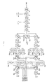
- a received signal emitted from the antenna is amplified after the filter 1a in an RF amplifier 2, the gain of which can be reduced by control F, e.g. 20 dB.
- the signal filtered in the filter 1b is taken to a mixer 3, where the intermediate frequency filtered from the mixing results thereof and of the local oscillator is divided after the intermediate amplifier 5 into two branches for producing I and Q signals.
- the I/Q signals (of sin and cos shape) are produced in the mixers 6a and 6b so that the incoming signal is mixed with the frequency from the second local oscillator in the mixers when the incoming local oscillator frequencies are at 90 degree phase shift to each other.
- the I/Q signal production is in itself known in the art, and it will not be referred to in the present context.
- the I and Q signals obtained as mixing results are amplified in amplifiers 7a and 7b, and the high frequencies are filtered from the amplified signals in filters 8a and 8b.
- the circuit hereinafter contains the very core of the invention.
- the signal path in both branches is divided into a plurality of branches, each of which being provided with an amplifier 9a, 10a, 11a, 12a; 9b, 10b, 11b, 12b.
- multiplexers 13a, 13b one amplifier may in both branches at a time be connected to the signal path, e.g. by a given multiplexer control the signal passes in the I branch through the amplifier 10b and in Q branch, through the amplifier 10a. Said amplifiers have equal gain.
- the signals will pass through other amplifiers, said amplifiers always having the equal gain, two and two, but it is understood that the amplifiers 9a-12a of the Q branch have different gains, as have also the amplifiers 9b-12b of the I branch.
- the gain of the amplifiers 10a and 10b could be e.g. 50 dB, the gain of the amplifiers 11a and 11b e.g. 18 dB, and the gain of the amplifiers 12a and 12b e.g. 2 dB.
- the above values are, in fact, gains of said amplifiers.
- a given amplifying step is hereby selected, which means a relative change of the gain.
- a signal selected from the 50 dB amplifier corresponds to a 0 dB gain step, that is maximum gain, and e.g. a signal from the 2 dB amplifier corresponds to the -48 dB gain step.
- selecting 34 dB and 18 dB amplifiers is equivalent to the gain step -16 dB and -32 dB. Different gains may, of course, be used.
- the multiplexers are controlled using digital control signals A and B, with which the multiplexer can be directed into four different positions.
- the control signals are obtained from the logic circuit of the telephone which is monitoring the signal level prior to the AD converters.
- a given control signal combination C, D and E produces an amplification step of equal magnitude from the attenuators 14a and 14b. After the attenuators 14a and 14b, the signals propagate through the amplifiers 16a and 16b to the output of the circuit.
- the gain of the amplifiers 16a and 16b could be e.g. 15 dB.
- the range may be further expanded by making the RF amplification 2 so controlable that its gain can be reduced by means of the logic control F e.g. in the amount of 20 dB.
- the logic control F e.g. in the amount of 20 dB.
- an 84 dB power range can be covered with control signals A, B, C, D, E, F at 2 dB intervals. In the GMS system, this is quite sufficient.
- an AGC amplifier circuit placed in the base band frequency parts is introduced.
- An AGC amplifier circuit placed in the base band frequency sections is in principle implementable in a remarkably simpler way by placing in the base band frequency section in succession logic-controlled amplifier/attenuator stages, the amplifying or attenuating steps thereof would be in 2, 4, 8, 16, 32 dB (and a 20 dB attenuation in the RF part).
- Another prob lem is related to change of DC levels caused by the offset voltages of the operational amplifiers conforming to the selected gain, if for the gain control system to select e.g. feedback gains in the operational amplifiers is used with the aid of analog switches.
- the effect of the circuit peaks has been eliminated by dividing the signal first into four branches, and by amplifying the level of each branch to correspond to the desired amplification step.
- the level of the signal selected with the multiplexer 13a and 13b is of equal magnitude as in the level of the circuit peak; therefore, the circuit peak causes no harm.
- the effect of the offset voltages can be eliminated using an AC circuit (capacitors) before the multiplexers.
- the smallest amplification steps may thereafter be produced by selecting from the resistance attenuator 14a, 14b a signal of the desired level using the multiplexer 15a, 15b.
- an AGC system of a digital radio telephone receiver is produced with which all amplification steps required in the GSM telephone can be produced without any drawbacks caused by the circuit peaks and changes of DC levels, and without the drawbacks which the AGC function placed in the intermediate frequency stages causes.
- the amplification steps are precise, and they are not dependent on temperature. Since most part of the gain and of the AGC function can be placed in the base band frequency parts, the gain of the RF stages and the intermediate frequency stages can be set to be considerably small (e.g. amounting to 20 dB), and consequently, a very simple and inexpensive filter can be used.
- the entire receiver can be made such that it occupies a very small space because most of the gain and the AGC function are placed in the base band frequency sections, which may be entirely integrated on silicon.
- the intermediate frequency sections have no gain control associated with the AGC; therefore, connecting a signal from the local oscillator to the intermediate frequency stages is not objectionable. In other words, the DC voltage levels of the I and Q branches do not vary because of the local oscillator signal connected to the intermediate frequency stages.
- the circuit is implementable in practice in a plurality of ways.
- more than four amplifiers may be provided, and the attenuator can be other than the resistance network.
Landscapes
- Circuits Of Receivers In General (AREA)
- Control Of Amplification And Gain Control (AREA)
- Input Circuits Of Receivers And Coupling Of Receivers And Audio Equipment (AREA)
- Mobile Radio Communication Systems (AREA)
- Digital Transmission Methods That Use Modulated Carrier Waves (AREA)
- Superheterodyne Receivers (AREA)
- Chemical Or Physical Treatment Of Fibers (AREA)
- Organic Low-Molecular-Weight Compounds And Preparation Thereof (AREA)
- Radio Relay Systems (AREA)
Applications Claiming Priority (2)
| Application Number | Priority Date | Filing Date | Title |
|---|---|---|---|
| FI894966 | 1989-10-18 | ||
| FI894966A FI88563C (fi) | 1989-10-18 | 1989-10-18 | Automatisk foerstaerkningregleringskoppling i radiotelefonens mottagare |
Publications (3)
| Publication Number | Publication Date |
|---|---|
| EP0424009A2 true EP0424009A2 (de) | 1991-04-24 |
| EP0424009A3 EP0424009A3 (en) | 1992-05-06 |
| EP0424009B1 EP0424009B1 (de) | 1996-03-06 |
Family
ID=8529188
Family Applications (1)
| Application Number | Title | Priority Date | Filing Date |
|---|---|---|---|
| EP90311062A Expired - Lifetime EP0424009B1 (de) | 1989-10-18 | 1990-10-09 | Automatische Verstärkungsregelungsschaltung für Funktelefonempfänger |
Country Status (6)
| Country | Link |
|---|---|
| EP (1) | EP0424009B1 (de) |
| JP (1) | JP3162700B2 (de) |
| AT (1) | ATE135146T1 (de) |
| DE (1) | DE69025697T2 (de) |
| ES (1) | ES2084664T3 (de) |
| FI (1) | FI88563C (de) |
Cited By (3)
| Publication number | Priority date | Publication date | Assignee | Title |
|---|---|---|---|---|
| JPH0511521U (ja) * | 1991-07-17 | 1993-02-12 | 富士通テン株式会社 | 直交復調回路 |
| FR2795259A1 (fr) * | 1999-06-15 | 2000-12-22 | Sagem | Telephone mobile ayant une chaine de numerisation a gain variable rapidement et procede de numerisation par un tel telephone |
| EP2073383A1 (de) | 2007-12-19 | 2009-06-24 | Sequans Communications | Verstärkeranordnung |
Families Citing this family (2)
| Publication number | Priority date | Publication date | Assignee | Title |
|---|---|---|---|---|
| JP2582828Y2 (ja) * | 1992-11-04 | 1998-10-15 | 富士通テン株式会社 | レベルコントロールダイレクト受信機 |
| WO2000051253A1 (fr) * | 1999-02-25 | 2000-08-31 | Mitsubishi Denki Kabushiki Kaisha | Unite de poste de radio |
Family Cites Families (2)
| Publication number | Priority date | Publication date | Assignee | Title |
|---|---|---|---|---|
| US4598252A (en) * | 1984-07-06 | 1986-07-01 | Itt Corporation | Variable gain power amplifier |
| US4792991A (en) * | 1986-04-03 | 1988-12-20 | Motorola, Inc. | FM receiver having improved audio quality in response to Rayleigh faded received signals |
-
1989
- 1989-10-18 FI FI894966A patent/FI88563C/fi active IP Right Grant
-
1990
- 1990-10-09 AT AT90311062T patent/ATE135146T1/de not_active IP Right Cessation
- 1990-10-09 EP EP90311062A patent/EP0424009B1/de not_active Expired - Lifetime
- 1990-10-09 ES ES90311062T patent/ES2084664T3/es not_active Expired - Lifetime
- 1990-10-09 DE DE69025697T patent/DE69025697T2/de not_active Expired - Lifetime
- 1990-10-17 JP JP27660190A patent/JP3162700B2/ja not_active Expired - Lifetime
Cited By (5)
| Publication number | Priority date | Publication date | Assignee | Title |
|---|---|---|---|---|
| JPH0511521U (ja) * | 1991-07-17 | 1993-02-12 | 富士通テン株式会社 | 直交復調回路 |
| FR2795259A1 (fr) * | 1999-06-15 | 2000-12-22 | Sagem | Telephone mobile ayant une chaine de numerisation a gain variable rapidement et procede de numerisation par un tel telephone |
| DE10029057C2 (de) * | 1999-06-15 | 2003-04-10 | Sagem | Mobiltelefon mit einer Digitalisierungskette mit rasch veränderlichem Verstärkungsgrad und Digitalisierungsverfahren durch ein solches Telefon |
| EP2073383A1 (de) | 2007-12-19 | 2009-06-24 | Sequans Communications | Verstärkeranordnung |
| US7994855B2 (en) | 2007-12-19 | 2011-08-09 | Sequans Communications Limited | Amplifier arrangement |
Also Published As
| Publication number | Publication date |
|---|---|
| JP3162700B2 (ja) | 2001-05-08 |
| ES2084664T3 (es) | 1996-05-16 |
| FI894966A0 (fi) | 1989-10-18 |
| ATE135146T1 (de) | 1996-03-15 |
| DE69025697T2 (de) | 1996-08-08 |
| JPH03208433A (ja) | 1991-09-11 |
| EP0424009A3 (en) | 1992-05-06 |
| FI88563B (fi) | 1993-02-15 |
| EP0424009B1 (de) | 1996-03-06 |
| FI88563C (fi) | 1993-05-25 |
| DE69025697D1 (de) | 1996-04-11 |
Similar Documents
| Publication | Publication Date | Title |
|---|---|---|
| US5233634A (en) | Automatic gain control circuit in a radio telephone receiver | |
| US6035008A (en) | Automatic gain control in direct sequence spread spectrum communication system | |
| US4553105A (en) | Multistage linear amplifier for a wide range of input signal levels | |
| EP0397445B1 (de) | Schaltung zur Bildung niedriger Leistungspegel in einem Funktelefonsender | |
| AU596134B2 (en) | Fm receiver with noise suppression during rayleigh faded received signals | |
| EP0464792A2 (de) | AGC-Schaltung einer FM-Eingangsstufe | |
| EP0856952A2 (de) | Verfahren und Schaltung zur Empfangssignalverarbeitung in einen Telekommunikationssystem | |
| KR100295223B1 (ko) | 수신기 | |
| EP0424009A2 (de) | Automatische Verstärkungsregelungsschaltung für Funktelefonempfänger | |
| US4064462A (en) | Acoustic feedback peak elimination unit | |
| WO1999046855A3 (en) | Radio receiver and gain controlled amplifier therefor | |
| EP0944166B1 (de) | Automatische dynamikbereich-steuerschaltung | |
| EP0667994B1 (de) | Verfahren und anordnung zur steuerung eines hochfrequenz-leistungsverstärkers | |
| JPH0470203A (ja) | フィードフォワード増幅器 | |
| US5042085A (en) | Radio frequency data communication band pass filter | |
| US5918166A (en) | Level control circuit for portable radio communication apparatus | |
| EP0660511A2 (de) | Automatische Verstärkungsregelung in Radioempfängern | |
| US6785524B2 (en) | Device and method for controlling the amplitude of signals | |
| JPH0537409A (ja) | 移動通信装置 | |
| KR890001276A (ko) | 정상 이득 제어를 하는 과왜곡(superdistorted)앰프회로 | |
| GB2437335A (en) | An efficient RF transmitter for high peak-to-average ratio (PAR) signals | |
| KR200173900Y1 (ko) | 수신 특성을 향상시킨 이동 단말기 | |
| JP2616098B2 (ja) | 電力増幅装置 | |
| JPH07336268A (ja) | デュアルモード無線機 | |
| JPH07283674A (ja) | 単チャンネル中間周波信号変換増幅器 |
Legal Events
| Date | Code | Title | Description |
|---|---|---|---|
| PUAI | Public reference made under article 153(3) epc to a published international application that has entered the european phase |
Free format text: ORIGINAL CODE: 0009012 |
|
| AK | Designated contracting states |
Kind code of ref document: A2 Designated state(s): AT BE CH DE DK ES FR GB GR IT LI LU NL SE |
|
| PUAL | Search report despatched |
Free format text: ORIGINAL CODE: 0009013 |
|
| AK | Designated contracting states |
Kind code of ref document: A3 Designated state(s): AT BE CH DE DK ES FR GB GR IT LI LU NL SE |
|
| 17P | Request for examination filed |
Effective date: 19921013 |
|
| 17Q | First examination report despatched |
Effective date: 19940922 |
|
| GRAA | (expected) grant |
Free format text: ORIGINAL CODE: 0009210 |
|
| AK | Designated contracting states |
Kind code of ref document: B1 Designated state(s): AT BE CH DE DK ES FR GB GR IT LI LU NL SE |
|
| PG25 | Lapsed in a contracting state [announced via postgrant information from national office to epo] |
Ref country code: CH Effective date: 19960306 Ref country code: LI Effective date: 19960306 Ref country code: GR Free format text: LAPSE BECAUSE OF FAILURE TO SUBMIT A TRANSLATION OF THE DESCRIPTION OR TO PAY THE FEE WITHIN THE PRESCRIBED TIME-LIMIT Effective date: 19960306 Ref country code: DK Effective date: 19960306 Ref country code: BE Effective date: 19960306 |
|
| REF | Corresponds to: |
Ref document number: 135146 Country of ref document: AT Date of ref document: 19960315 Kind code of ref document: T |
|
| REF | Corresponds to: |
Ref document number: 69025697 Country of ref document: DE Date of ref document: 19960411 |
|
| ET | Fr: translation filed | ||
| REG | Reference to a national code |
Ref country code: ES Ref legal event code: FG2A Ref document number: 2084664 Country of ref document: ES Kind code of ref document: T3 |
|
| ITF | It: translation for a ep patent filed | ||
| REG | Reference to a national code |
Ref country code: CH Ref legal event code: PL |
|
| PG25 | Lapsed in a contracting state [announced via postgrant information from national office to epo] |
Ref country code: LU Free format text: LAPSE BECAUSE OF NON-PAYMENT OF DUE FEES Effective date: 19961031 |
|
| PLBE | No opposition filed within time limit |
Free format text: ORIGINAL CODE: 0009261 |
|
| STAA | Information on the status of an ep patent application or granted ep patent |
Free format text: STATUS: NO OPPOSITION FILED WITHIN TIME LIMIT |
|
| 26N | No opposition filed | ||
| REG | Reference to a national code |
Ref country code: GB Ref legal event code: IF02 |
|
| REG | Reference to a national code |
Ref country code: GB Ref legal event code: 732E |
|
| PGFP | Annual fee paid to national office [announced via postgrant information from national office to epo] |
Ref country code: SE Payment date: 20091007 Year of fee payment: 20 Ref country code: ES Payment date: 20091117 Year of fee payment: 20 Ref country code: DE Payment date: 20091001 Year of fee payment: 20 Ref country code: AT Payment date: 20091013 Year of fee payment: 20 |
|
| PGFP | Annual fee paid to national office [announced via postgrant information from national office to epo] |
Ref country code: NL Payment date: 20091004 Year of fee payment: 20 |
|
| PGFP | Annual fee paid to national office [announced via postgrant information from national office to epo] |
Ref country code: GB Payment date: 20091007 Year of fee payment: 20 Ref country code: FR Payment date: 20091029 Year of fee payment: 20 Ref country code: IT Payment date: 20091016 Year of fee payment: 20 |
|
| REG | Reference to a national code |
Ref country code: NL Ref legal event code: V4 Effective date: 20101009 |
|
| REG | Reference to a national code |
Ref country code: GB Ref legal event code: PE20 Expiry date: 20101008 |
|
| EUG | Se: european patent has lapsed | ||
| PG25 | Lapsed in a contracting state [announced via postgrant information from national office to epo] |
Ref country code: NL Free format text: LAPSE BECAUSE OF EXPIRATION OF PROTECTION Effective date: 20101009 |
|
| PG25 | Lapsed in a contracting state [announced via postgrant information from national office to epo] |
Ref country code: GB Free format text: LAPSE BECAUSE OF EXPIRATION OF PROTECTION Effective date: 20101008 |
|
| REG | Reference to a national code |
Ref country code: ES Ref legal event code: FD2A Effective date: 20120424 |
|
| PG25 | Lapsed in a contracting state [announced via postgrant information from national office to epo] |
Ref country code: ES Free format text: LAPSE BECAUSE OF EXPIRATION OF PROTECTION Effective date: 20101010 |
|
| PG25 | Lapsed in a contracting state [announced via postgrant information from national office to epo] |
Ref country code: DE Free format text: LAPSE BECAUSE OF EXPIRATION OF PROTECTION Effective date: 20101009 |