EP2079092A1 - Vorrichtung und Verfahren zur Stromversorgung einer Elektronenquelle und Elektronenquelle mit Sekundäremission unter Ionenbombardierung - Google Patents
Vorrichtung und Verfahren zur Stromversorgung einer Elektronenquelle und Elektronenquelle mit Sekundäremission unter Ionenbombardierung Download PDFInfo
- Publication number
- EP2079092A1 EP2079092A1 EP08290026A EP08290026A EP2079092A1 EP 2079092 A1 EP2079092 A1 EP 2079092A1 EP 08290026 A EP08290026 A EP 08290026A EP 08290026 A EP08290026 A EP 08290026A EP 2079092 A1 EP2079092 A1 EP 2079092A1
- Authority
- EP
- European Patent Office
- Prior art keywords
- pulse
- generating
- voltage
- positive pulses
- electron source
- Prior art date
- Legal status (The legal status is an assumption and is not a legal conclusion. Google has not performed a legal analysis and makes no representation as to the accuracy of the status listed.)
- Granted
Links
Images

Classifications
-
- H—ELECTRICITY
- H01—ELECTRIC ELEMENTS
- H01J—ELECTRIC DISCHARGE TUBES OR DISCHARGE LAMPS
- H01J3/00—Details of electron-optical or ion-optical arrangements common to two or more basic types of discharge tubes or lamps
- H01J3/02—Electron guns
- H01J3/021—Electron guns using a field emission, photo emission, or secondary emission electron source
-
- H—ELECTRICITY
- H01—ELECTRIC ELEMENTS
- H01J—ELECTRIC DISCHARGE TUBES OR DISCHARGE LAMPS
- H01J27/00—Ion beam tubes
- H01J27/02—Ion sources; Ion guns
- H01J27/20—Ion sources; Ion guns using particle beam bombardment, e.g. ionisers
- H01J27/205—Ion sources; Ion guns using particle beam bombardment, e.g. ionisers with electrons, e.g. electron impact ionisation, electron attachment
-
- H—ELECTRICITY
- H01—ELECTRIC ELEMENTS
- H01J—ELECTRIC DISCHARGE TUBES OR DISCHARGE LAMPS
- H01J33/00—Discharge tubes with provision for emergence of electrons or ions from the vessel; Lenard tubes
-
- H—ELECTRICITY
- H01—ELECTRIC ELEMENTS
- H01J—ELECTRIC DISCHARGE TUBES OR DISCHARGE LAMPS
- H01J2237/00—Discharge tubes exposing object to beam, e.g. for analysis treatment, etching, imaging
- H01J2237/26—Electron or ion microscopes
- H01J2237/262—Non-scanning techniques
- H01J2237/2623—Field-emission microscopes
- H01J2237/2626—Pulsed source
Definitions
- the invention relates to the field of pulsed sources of electrons and devices using such sources, including gas lasers with electron excitation or pre-ionization pulsed under X-rays.
- a pulsed source of electrons emits a beam of electrons under the effect of ion bombardment.
- the device comprises an ionization chamber and an acceleration chamber communicating with the ionization chamber by a grid.
- a preliminary discharge occurs in the ionization chamber.
- Part of the positive ions thus created is accelerated to a cathode located in the acceleration chamber.
- the accelerated ions bombard the cathode and cause the secondary emission of electrons.
- the secondary electrons accelerated by being pushed back by the negative voltage applied to the cathode then form an electron beam extracted by the grid between the two chambers.
- the triggering of the discharge in the ionization chamber tends to become increasingly difficult as and when the device is used.
- the discharge is therefore triggered later and later and may occur at the same time as the negative voltage pulse applied to the cathode.
- Simultaneous application of the positive voltage in the ionization chamber and the negative voltage in the acceleration chamber presents a danger of failure or even destruction for the device and for the systems in which the device is implemented.
- the delayed triggering of the discharge causes in any case the degradation of the characteristics of the electron beam obtained at the output of the source.
- the natural and therefore uncontrolled delay in triggering the discharge in the ionization chamber is unsatisfactory.
- the present invention aims to overcome the disadvantages mentioned above.
- the object of the invention is in particular to obtain a stable triggering of the electronic source that is relatively independent of the operating conditions, such as the aging of the source.
- the power supply device of a secondary emission electron source under ion bombardment in a low pressure chamber comprises a control input, two high voltage outputs, means for generating a plurality of positive pulses on a high output. voltage and means for generating a negative pulse on the other high voltage output after at least a portion of the positive pulses. Generating a plurality of positive pulses that can be applied to an ionization chamber electrode makes it easier to trigger the discharge.
- the device comprises means for generating a delay between the end of operation means for generating a plurality of positive pulses and the start of operation of the means for generating a negative pulse.
- the delay can be constant or adjustable to suit operating parameters, including pressure, molecular weight of the gas, etc.
- the means for generating a plurality of positive pulses is configured so that the first pulse has a voltage greater than the voltage of subsequent pulses. Even if the first discharge in the ionization chamber is delayed, the trip delay stabilizes quickly.
- the negative pulse can then be controlled after a delay D1 has elapsed since the command to trigger the last positive pulse, the delay D2 between the command of the last positive pulse and the triggering of the last discharge in the chamber. of ionization that can be accurately known.
- the method for powering a ion-bombarded secondary emission electron source in a low-pressure chamber includes a step of generating a plurality of positive pulses on a high voltage output and a step of generating a a negative pulse on another high voltage output after at least a portion of the positive pulses.
- a non-zero delay separates the end of the last positive pulse from the series of pulses positive and the beginning of the negative impulse. This ensures the safety of the device.
- the peak voltage of the first positive pulse is greater than the peak voltage of the subsequent positive pulses.
- the first discharge is facilitated with a first high voltage pulse.
- the discharge can be easily obtained at subsequent pulses with a lower voltage. Energy consumption is reduced and the aging of the power supply is lower.
- the peak voltage of the subsequent positive pulses is substantially equal.
- the duration of the next positive pulses is substantially constant.
- the voltage of at least one pulse can be increased during aging.
- the electron source comprises a low pressure chamber, an acceleration chamber, a cathode disposed in the acceleration chamber, an anode disposed in the low pressure chamber and a power supply device provided with two high voltage outputs, one connected to the anode and the other to the cathode.
- the power supply device includes means for generating a plurality of positive pulses and means for generating a negative pulse after the positive pulses.
- the source includes a control module of the means for generating a plurality of positive pulses and means for generating a negative pulse.
- the control module can be configured to calculate the delay to avoid simultaneous positive pulse and negative pulse.
- the lifetime of the electron source is also increased by reducing the aging of the power supply and the ionization chamber. The cost of using the electron source is thus optimized.
- auxiliary source at the cathode possibly coupled with a magnetic electron confinement system.
- life of the source is then limited because of the vaporization of the hot anode and the deposition of vaporized materials that forms on the walls of the ionization chamber causing degradation of the operation of the source.
- the electron source 1 comprises an acceleration chamber 2 and an ionization chamber 3 defined by an enclosure 4.
- the ionization chamber 3 can be elongated in a main direction.
- the enclosure 4 comprises an outer casing 5 and an inner wall 6 separating the chambers 2 and 3.
- the enclosure 4 may be made of metal, for example based on brass or stainless steel.
- the internal walls defining on the one hand the acceleration chamber 2 and on the other hand the ionization chamber 3 may be covered with a metal or a metal alloy adapted to the application in question, particularly in terms of voltage electric applied and gas in the enclosure 4, including the nature and pressure of the gas.
- a coating based on aluminum or nickel may cover the walls of the acceleration chamber 2, and / or the walls of the ionization chamber 3.
- the acceleration chamber 2 and the ionization chamber 3 are placed in communication by a passage 7 in the form of a through hole formed in the inner wall 6.
- the passage 7 may be provided with a gate 8, in general metallic.
- An outlet 9 is provided in an outer wall of the ionization chamber 3 opposite the inner wall 6.
- the outlet 9 may be open or provided with a grid, particularly in the case where a gas of a similar nature and similar pressure is present in the chamber 4 and around the chamber 4.
- the outlet 9 is generally provided with a shutter, not shown , for example in the form of a piece of synthetic material, impervious to gas and permeable at least in part to the electrons to allow the output of the electron flow generated in the source 1.
- the shutter can also be covered with a metal layer, especially based on high atomic mass metal for example greater than 50 to generate X-rays under the effect of electron bombardment.
- the electron source 1 comprises a cathode 10 mounted in the acceleration chamber 2.
- the cathode 10 may be fixed or rotating.
- the cathode 10 may be made from stainless steel or aluminum alloy.
- the cathode 10 may be in the form of a disk providing a surface 10a plane facing the passage 7 or a cylinder.
- the passages 7 and 9 and the flat surface 10a of the cathode 10 are aligned.
- the cathode 10 is supported by a gas-tight insulator 11 fixed in a hole in an outer wall of the casing 5.
- the insulator 11 can also be aligned with the openings 7 and 9.
- the insulator 11 forms a bushing electrical supply allowing the power supply of the cathode 10 from the outside of the envelope 5.
- the electron source 1 comprises an anode 12 disposed in the ionization chamber 3.
- the anode 12 may be in the form of one or more wires, elongated along the main direction of the chamber 3.
- the wire may be fed at both ends for increased homogeneity of the electric field.
- the anode 12 is supported by a sealed insulator 13 attached to a side wall of the outer casing 5 and providing gastightness and electrical crossing.
- the anode 12 is offset with respect to the alignment of the openings 7 and 9.
- the electron source 1 comprises a power supply 14 comprising a supply module 15 of the cathode 10, a supply module 16 of the anode 12 and a control module 17.
- the supply module 15 and the module 16 may be of the type illustrated on the figure 5 .
- the control module 17 is configured to generate pulse control signals temporally offset between the signal sent to the power supply module 16 and the signal sent to the power supply module 15. Said time offset can be made the object of adjustment according to the gas pressure in the acceleration chamber 2 and ionization 3 and the nature of the gas or gas mixture, in particular the atomic mass.
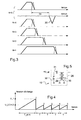
- the control module 17 sends a signal 18, see figure 2 , to the power supply module 16.
- the signal 18 is in the form of a plurality of rectangular signals, in particular five in number. The number of pulses can be increased in time to compensate for the aging of the source 1.
- the control module 17 sends a signal 19 to the power supply module 15 to apply a high negative voltage to the cathode 10.
- the signal 19 can be synchronized to the end of the signal 18, possibly with a delay not shown, or be sent before the end of the signal 18 but after the start.
- the number N designates the rank of the applied voltage pulse.
- the current discharge occurs only after the application of a high voltage for a relatively long time. Then this high voltage duration prior to the discharge decreases from the first to the fourth pulse and remains substantially constant at the fifth pulse.
- the time scales for each pulse have been vertically aligned for the purposes of the drawing.
- the rank N pulse occurs after the N-1 rank pulse.
- the control module 17 sends to the power supply module 15 the signal 19 which causes the application of a negative high voltage in the form of the curve 20, to the cathode 10.
- the negative voltage pulse 20 applied to the cathode 10 starts after a duration D4 elapsed since the end of the maximum value of the positive voltage pulse on the anode 12, or in other words, since substantially the end of the last control pulse of the signal 18 received by the power supply module 16.
- said duration can be determined by the operating conditions such as the value of the voltage, the gas pressure, the nature of the gas, the distance between the anode 12 and the walls of the ionization chamber 3, etc.
- the duration of the nth positive voltage pulse can be estimated or measured experimentally.
- the control module 17 can be configured, simply and economically, to generate the control pulse 19 after a duration equal to the sum of the duration D4 and the duration of the positive voltage pulse has elapsed. since the end of the command pulse 18
- the control module 17 generates a positive voltage control signal comprising a first pulse of longer duration than the duration of the other pulses of the signal 18 from which a longer charging time of the power supply module 16 and a voltage of the first positive voltage pulse applied to the electrode 12 higher than that of rows 2 and more.
- the Applicant has indeed noticed that the first discharge is particularly difficult to obtain and can be obtained more easily and faster with a higher voltage.
- the impulses of Positive voltage of rows 2 and higher can be obtained with a lower voltage resulting in a lower load of the power supply module 16 which undergoes reduced wear here. It is possible to choose a voltage of the first optimal pulse for priming the first discharge and a subsequent pulse voltage optimal for the stability of the discharges.
- the voltage of the following pulses may be between 80 and 100% of the voltage of the first pulse.
- the first discharge is triggered by a higher voltage than the other discharges.
- the multi-pulse triggered electron source provides a stable electron beam with reduced aging largely free of factors such as the duration and conditions of its use.
- the voltage of the first pulse, the voltage of the subsequent pulses and / or the number of subsequent pulses can be increased over time.
- a button or an automatic control can be provided for this purpose. Maintenance is very easy.
- the acceleration 2 and ionization chambers 3 are filled with a gas, for example helium at low pressure, for example between 1 and 20 Pascals.
- a gas for example helium at low pressure, for example between 1 and 20 Pascals.
- the application of a positive voltage on the anode 12, the enclosure 4 being maintained in the ground, causes a voltage pulse discharge.
- the electric discharge in the ionization chamber 3 containing gas causes the emission of positive ions.
- the impulse of voltage on the anode 12 ceases and the negative voltage pulse on the cathode 10 occurs.
- the positive ions are then attracted by the cathode 10, pass through the passage 7 to come to bombard the flat surface 10a of the electrode 10 along the trajectory of the arrow 21.
- the ion bombardment of the cathode 10 causes the emission of electrons which undergo a repulsive effect of the cathode 10 due to the high negative voltage applied by the power supply module 15.
- the electrons are accelerated according to the trajectory of the arrow 22, pass through the passage 7 and then the exit 9 and thus provide a beam of electrons.
- the power supply 15 comprises a pulse transformer 28 provided with a primary 29 and a secondary 30.
- the primary 29 of the pulse transformer 28 is connected firstly to ground and secondly to a capacitor 31.
- the capacitor 31 is connected to a voltage source U 0 and to a switch 32.
- the switch 32 is also connected to the ground in order to be able to short-circuit the capacitor 31 and the primary 29.
- the secondary 30 is connected on the one hand to the mass of the power supply and on the other hand to the cathode 10 of the electron source 1.
- the power supply 15 may also comprise, parallel to the secondary 30, an auxiliary voltage source supplying the bias voltage and connected firstly to the ground of the supply and secondly to the common point between the secondary 30 and the 3.
- a protection may be arranged in series with the auxiliary source to limit the flow of current.
- the protection may comprise at least one diode, a capacitor and / or an inductor.
- a sensor current can be provided at the output of the power supply 15 for measuring the current consumed in the ionization chamber 2.
- the switch 32 forms an open circuit.
- the capacitor 31 is charged to the voltage U 0 .
- the auxiliary voltage source can maintain the cathode 10 at the positive bias voltage.
- a diode may be disposed between the secondary 30 and the common point to the protection and the cathode 10. After closing the switch 32 short-circuiting the capacitor 31 and the primary 29 of the transformer 28, a negative high voltage pulse -U qun is supplied by the secondary 30 of transformer 28 and applied to the cathode 10.
- the electron source 1 can be modeled electrically by a parasitic capacitance C gun .
- the parasitic capacitance C gun can be considerably reduced due to the absence, or in the absence of the very small quantity, of the plasma in the acceleration chamber 2 during the first ionization step. If plasma is present in the acceleration chamber 2, the polarization of the plasma generates a high parasitic capacitance. Thanks to the application of the positive bias voltage which prevents the entry of positive ions from the plasma into the acceleration chamber 2 during the first step, the acceleration chamber 2 is substantially free of plasma at the time of the application of the negative high voltage -U gun to the cathode 10. The parasitic capacitance C gun remains low.
- the charging voltage U 0 of the power supply 15 can be reduced. Alternatively, the transformation ratio of the transformer 28 can be reduced.
Landscapes
- Chemical & Material Sciences (AREA)
- Engineering & Computer Science (AREA)
- Combustion & Propulsion (AREA)
- Electron Sources, Ion Sources (AREA)
Priority Applications (9)
| Application Number | Priority Date | Filing Date | Title |
|---|---|---|---|
| AT08290026T ATE477585T1 (de) | 2008-01-11 | 2008-01-11 | Vorrichtung und verfahren zur stromversorgung einer elektronenquelle und elektronenquelle mit sekundäremission unter ionenbombardierung |
| DE602008002138T DE602008002138D1 (de) | 2008-01-11 | 2008-01-11 | Vorrichtung und Verfahren zur Stromversorgung einer Elektronenquelle und Elektronenquelle mit Sekundäremission unter Ionenbombardierung |
| EP08290026A EP2079092B1 (de) | 2008-01-11 | 2008-01-11 | Vorrichtung und Verfahren zur Stromversorgung einer Elektronenquelle und Elektronenquelle mit Sekundäremission unter Ionenbombardierung |
| JP2010541819A JP5340309B2 (ja) | 2008-01-11 | 2009-01-08 | 電子源に電力を供給する装置および方法、ならびにイオン照射が誘導される二次放出電子源 |
| KR1020107017749A KR20100134558A (ko) | 2008-01-11 | 2009-01-08 | 전자 소스에 전력을 공급하는 장치 및 방법과 이온 충격 유도 2차 방출 전자 소스 |
| CN2009801019286A CN101952927B (zh) | 2008-01-11 | 2009-01-08 | 向电子源供电的设备和方法以及离子轰击致二次发射电子源 |
| US12/812,245 US8664863B2 (en) | 2008-01-11 | 2009-01-08 | Device and method of supplying power to an electron source, and ion-bombardment-induced secondary-emission electron source |
| PCT/FR2009/000017 WO2009112668A1 (fr) | 2008-01-11 | 2009-01-08 | Dispositif et procédé d'alimentation électrique d'une source d'électrons et source d'électrons à émission secondaire sous bombardement ionique |
| TW98100594A TWI470919B (zh) | 2008-01-11 | 2009-01-09 | An electron source and a secondary emission electron source under an ion impact |
Applications Claiming Priority (1)
| Application Number | Priority Date | Filing Date | Title |
|---|---|---|---|
| EP08290026A EP2079092B1 (de) | 2008-01-11 | 2008-01-11 | Vorrichtung und Verfahren zur Stromversorgung einer Elektronenquelle und Elektronenquelle mit Sekundäremission unter Ionenbombardierung |
Publications (2)
| Publication Number | Publication Date |
|---|---|
| EP2079092A1 true EP2079092A1 (de) | 2009-07-15 |
| EP2079092B1 EP2079092B1 (de) | 2010-08-11 |
Family
ID=39494285
Family Applications (1)
| Application Number | Title | Priority Date | Filing Date |
|---|---|---|---|
| EP08290026A Active EP2079092B1 (de) | 2008-01-11 | 2008-01-11 | Vorrichtung und Verfahren zur Stromversorgung einer Elektronenquelle und Elektronenquelle mit Sekundäremission unter Ionenbombardierung |
Country Status (9)
| Country | Link |
|---|---|
| US (1) | US8664863B2 (de) |
| EP (1) | EP2079092B1 (de) |
| JP (1) | JP5340309B2 (de) |
| KR (1) | KR20100134558A (de) |
| CN (1) | CN101952927B (de) |
| AT (1) | ATE477585T1 (de) |
| DE (1) | DE602008002138D1 (de) |
| TW (1) | TWI470919B (de) |
| WO (1) | WO2009112668A1 (de) |
Cited By (1)
| Publication number | Priority date | Publication date | Assignee | Title |
|---|---|---|---|---|
| EP3196918A1 (de) | 2016-01-19 | 2017-07-26 | Laser Systems and Solutions of Europe | Niederdruckionenplasmaentladungsquelle mit draht und anwendung in einer elektronenquelle mit sekundäremission |
Families Citing this family (2)
| Publication number | Priority date | Publication date | Assignee | Title |
|---|---|---|---|---|
| US10338131B2 (en) * | 2015-11-24 | 2019-07-02 | Texas Instruments Incorporated | System and method for high voltage stress testing plurality of parallel units |
| CN108173450B (zh) * | 2018-02-06 | 2024-03-12 | 中国工程物理研究院流体物理研究所 | 一种集高压短脉冲预电离一体化高功率双极性脉冲形成电路 |
Citations (5)
| Publication number | Priority date | Publication date | Assignee | Title |
|---|---|---|---|---|
| FR2204882A1 (de) | 1972-10-30 | 1974-05-24 | Onera (Off Nat Aerospatiale) | |
| FR2312104A1 (fr) * | 1975-05-19 | 1976-12-17 | Hughes Aircraft Co | Canon generateur d'electrons excite par un plasma |
| FR2591035A1 (fr) | 1985-11-29 | 1987-06-05 | Onera (Off Nat Aerospatiale) | Canon a electrons operant par emission secondaire sous bombardement ionique |
| FR2615324A1 (fr) * | 1987-03-30 | 1988-11-18 | Rpc Ind | Canon a electrons a plasma ionique et procede pour pr oduire des electrons secondaires a partir d'un tel canon |
| US5841235A (en) * | 1996-05-31 | 1998-11-24 | Forschungszentrum Karlsruhe Gmbh | Source for the generation of large area pulsed ion and electron beams |
Family Cites Families (10)
| Publication number | Priority date | Publication date | Assignee | Title |
|---|---|---|---|---|
| DE58901620D1 (de) * | 1988-04-08 | 1992-07-16 | Siemens Ag | Plasma-roentgenroehre, insbesondere zur roentgen-vorionisierung von gaslasern, verfahren zur erzeugung von roentgenstrahlung mit einer solchen roentgenroehre und verwendung letzterer. |
| US5055748A (en) * | 1990-05-30 | 1991-10-08 | Integrated Applied Physics Inc. | Trigger for pseudospark thyratron switch |
| US5057740A (en) * | 1990-05-31 | 1991-10-15 | Integrated Applied Physics, Inc. | Photoemissive trigger for backlighted thyratron switches |
| JPH05211052A (ja) * | 1992-01-30 | 1993-08-20 | Toshiba Corp | パルス電子銃 |
| JPH08236053A (ja) * | 1995-02-28 | 1996-09-13 | Toshiba Corp | 電子銃 |
| JP3135864B2 (ja) * | 1997-05-27 | 2001-02-19 | 住友重機械工業株式会社 | イオン・プラズマ型電子銃とその制御方法 |
| US5910886A (en) * | 1997-11-07 | 1999-06-08 | Sierra Applied Sciences, Inc. | Phase-shift power supply |
| US6182604B1 (en) * | 1999-10-27 | 2001-02-06 | Varian Semiconductor Equipment Associates, Inc. | Hollow cathode for plasma doping system |
| US7663319B2 (en) * | 2004-02-22 | 2010-02-16 | Zond, Inc. | Methods and apparatus for generating strongly-ionized plasmas with ionizational instabilities |
| US20060121704A1 (en) * | 2004-12-07 | 2006-06-08 | Varian Semiconductor Equipment Associates, Inc. | Plasma ion implantation system with axial electrostatic confinement |
-
2008
- 2008-01-11 DE DE602008002138T patent/DE602008002138D1/de active Active
- 2008-01-11 AT AT08290026T patent/ATE477585T1/de not_active IP Right Cessation
- 2008-01-11 EP EP08290026A patent/EP2079092B1/de active Active
-
2009
- 2009-01-08 CN CN2009801019286A patent/CN101952927B/zh active Active
- 2009-01-08 JP JP2010541819A patent/JP5340309B2/ja active Active
- 2009-01-08 KR KR1020107017749A patent/KR20100134558A/ko not_active Ceased
- 2009-01-08 WO PCT/FR2009/000017 patent/WO2009112668A1/fr not_active Ceased
- 2009-01-08 US US12/812,245 patent/US8664863B2/en not_active Expired - Fee Related
- 2009-01-09 TW TW98100594A patent/TWI470919B/zh active
Patent Citations (5)
| Publication number | Priority date | Publication date | Assignee | Title |
|---|---|---|---|---|
| FR2204882A1 (de) | 1972-10-30 | 1974-05-24 | Onera (Off Nat Aerospatiale) | |
| FR2312104A1 (fr) * | 1975-05-19 | 1976-12-17 | Hughes Aircraft Co | Canon generateur d'electrons excite par un plasma |
| FR2591035A1 (fr) | 1985-11-29 | 1987-06-05 | Onera (Off Nat Aerospatiale) | Canon a electrons operant par emission secondaire sous bombardement ionique |
| FR2615324A1 (fr) * | 1987-03-30 | 1988-11-18 | Rpc Ind | Canon a electrons a plasma ionique et procede pour pr oduire des electrons secondaires a partir d'un tel canon |
| US5841235A (en) * | 1996-05-31 | 1998-11-24 | Forschungszentrum Karlsruhe Gmbh | Source for the generation of large area pulsed ion and electron beams |
Cited By (3)
| Publication number | Priority date | Publication date | Assignee | Title |
|---|---|---|---|---|
| EP3196918A1 (de) | 2016-01-19 | 2017-07-26 | Laser Systems and Solutions of Europe | Niederdruckionenplasmaentladungsquelle mit draht und anwendung in einer elektronenquelle mit sekundäremission |
| WO2017125315A1 (en) | 2016-01-19 | 2017-07-27 | Laser Systems & Solutions Of Europe | Low pressure wire ion plasma discharge source, and application to electron source with secondary emission |
| US10763070B2 (en) | 2016-01-19 | 2020-09-01 | Laser Systems & Solutions Of Europe | Low pressure wire ion plasma discharge source, and application to electron source with secondary emission |
Also Published As
| Publication number | Publication date |
|---|---|
| KR20100134558A (ko) | 2010-12-23 |
| CN101952927A (zh) | 2011-01-19 |
| JP5340309B2 (ja) | 2013-11-13 |
| US20110057565A1 (en) | 2011-03-10 |
| US8664863B2 (en) | 2014-03-04 |
| CN101952927B (zh) | 2012-10-17 |
| DE602008002138D1 (de) | 2010-09-23 |
| EP2079092B1 (de) | 2010-08-11 |
| WO2009112668A1 (fr) | 2009-09-17 |
| TWI470919B (zh) | 2015-01-21 |
| ATE477585T1 (de) | 2010-08-15 |
| JP2011509512A (ja) | 2011-03-24 |
| TW200939611A (en) | 2009-09-16 |
Similar Documents
| Publication | Publication Date | Title |
|---|---|---|
| EP2715131B1 (de) | Halleffekt-schubdüse | |
| EP2079092B1 (de) | Vorrichtung und Verfahren zur Stromversorgung einer Elektronenquelle und Elektronenquelle mit Sekundäremission unter Ionenbombardierung | |
| Miki et al. | Guiding of electrical discharges under atmospheric air by ultraviolet laser‐produced plasma channel | |
| EP0362946A1 (de) | Die Rückbeschleunigung von Sekundärelektronen begrenzende Ionenextraktions- und -beschleunigungseinrichtung in einer abgeschmolzenen Hochflup-Neutronenröhre | |
| WO2005090632A1 (fr) | Depot par pulverisation cathodique magnetron en regime impulsionnel avec preionisation | |
| EP3420636B1 (de) | Stromversorgungssystem für eine elektrisches halleffekt-strahlruder | |
| EP3051101B1 (de) | Hochenergie-zündunganlage, insbesondere für gasturbine | |
| FR2984028A1 (fr) | Eclateur haute tension a amorcage par laser comportant une cathode en materiau refractaire poreux a charge photoemissive | |
| FR2472830A1 (fr) | Dispositif de commande de conduction electrique en mode a champs croises en plasma | |
| EP2227819B1 (de) | Elektronenpumpquelle, stromversorgungsverfahren für eine elektronenpumpquelle und verfahren zur steuerung einer elektronenpumpquelle | |
| You et al. | A study of the plasma electronegativity in an argon–oxygen pulsed-dc sputter magnetron | |
| Sorokin | Electron beam formation in an anomalous glow discharge | |
| EP3574719A1 (de) | System zur erzeugung eines plasmastrahls von metallionen | |
| EP0362945A1 (de) | Einrichtung zur Verbesserung der Penning-Ionenquelle in einer Neutronenröhre | |
| EP3476015B1 (de) | Leistungsverstärker | |
| EP0159214A1 (de) | Elektronenstrahl-Installation zur Metallbearbeitung | |
| FR3147681A1 (fr) | Generateur de haute puissance pulse declenche par une impulsion de rayonnement ionisant. | |
| EP0497684A1 (de) | Elektrische Stromversorgung für Laser | |
| Labruyère et al. | Q-switching of a microchip laser using a plasma prism | |
| Losev et al. | The development of a long-pulse excimer laser system | |
| FR2513448A1 (fr) | Laser a impulsion a vapeurs de substances | |
| Losev et al. | Large aperture excimer laser system | |
| FR3062951A1 (fr) | Source d'ions positifs pour un spectrometre de masse de terrain | |
| BE500369A (de) |
Legal Events
| Date | Code | Title | Description |
|---|---|---|---|
| PUAI | Public reference made under article 153(3) epc to a published international application that has entered the european phase |
Free format text: ORIGINAL CODE: 0009012 |
|
| AK | Designated contracting states |
Kind code of ref document: A1 Designated state(s): AT BE BG CH CY CZ DE DK EE ES FI FR GB GR HR HU IE IS IT LI LT LU LV MC MT NL NO PL PT RO SE SI SK TR |
|
| AX | Request for extension of the european patent |
Extension state: AL BA MK RS |
|
| 17P | Request for examination filed |
Effective date: 20090912 |
|
| GRAP | Despatch of communication of intention to grant a patent |
Free format text: ORIGINAL CODE: EPIDOSNIGR1 |
|
| AKX | Designation fees paid |
Designated state(s): AT BE BG CH CY CZ DE DK EE ES FI FR GB GR HR HU IE IS IT LI LT LU LV MC MT NL NO PL PT RO SE SI SK TR |
|
| GRAS | Grant fee paid |
Free format text: ORIGINAL CODE: EPIDOSNIGR3 |
|
| GRAA | (expected) grant |
Free format text: ORIGINAL CODE: 0009210 |
|
| AK | Designated contracting states |
Kind code of ref document: B1 Designated state(s): AT BE BG CH CY CZ DE DK EE ES FI FR GB GR HR HU IE IS IT LI LT LU LV MC MT NL NO PL PT RO SE SI SK TR |
|
| REG | Reference to a national code |
Ref country code: GB Ref legal event code: FG4D Free format text: NOT ENGLISH |
|
| REG | Reference to a national code |
Ref country code: CH Ref legal event code: EP |
|
| REG | Reference to a national code |
Ref country code: IE Ref legal event code: FG4D Free format text: LANGUAGE OF EP DOCUMENT: FRENCH |
|
| REF | Corresponds to: |
Ref document number: 602008002138 Country of ref document: DE Date of ref document: 20100923 Kind code of ref document: P |
|
| REG | Reference to a national code |
Ref country code: CH Ref legal event code: NV Representative=s name: KATZAROV S.A. |
|
| REG | Reference to a national code |
Ref country code: NL Ref legal event code: T3 |
|
| LTIE | Lt: invalidation of european patent or patent extension |
Effective date: 20100811 |
|
| PG25 | Lapsed in a contracting state [announced via postgrant information from national office to epo] |
Ref country code: NO Free format text: LAPSE BECAUSE OF FAILURE TO SUBMIT A TRANSLATION OF THE DESCRIPTION OR TO PAY THE FEE WITHIN THE PRESCRIBED TIME-LIMIT Effective date: 20101111 Ref country code: LT Free format text: LAPSE BECAUSE OF FAILURE TO SUBMIT A TRANSLATION OF THE DESCRIPTION OR TO PAY THE FEE WITHIN THE PRESCRIBED TIME-LIMIT Effective date: 20100811 Ref country code: FI Free format text: LAPSE BECAUSE OF FAILURE TO SUBMIT A TRANSLATION OF THE DESCRIPTION OR TO PAY THE FEE WITHIN THE PRESCRIBED TIME-LIMIT Effective date: 20100811 Ref country code: AT Free format text: LAPSE BECAUSE OF FAILURE TO SUBMIT A TRANSLATION OF THE DESCRIPTION OR TO PAY THE FEE WITHIN THE PRESCRIBED TIME-LIMIT Effective date: 20100811 |
|
| PG25 | Lapsed in a contracting state [announced via postgrant information from national office to epo] |
Ref country code: HR Free format text: LAPSE BECAUSE OF FAILURE TO SUBMIT A TRANSLATION OF THE DESCRIPTION OR TO PAY THE FEE WITHIN THE PRESCRIBED TIME-LIMIT Effective date: 20100811 Ref country code: IS Free format text: LAPSE BECAUSE OF FAILURE TO SUBMIT A TRANSLATION OF THE DESCRIPTION OR TO PAY THE FEE WITHIN THE PRESCRIBED TIME-LIMIT Effective date: 20101211 Ref country code: PL Free format text: LAPSE BECAUSE OF FAILURE TO SUBMIT A TRANSLATION OF THE DESCRIPTION OR TO PAY THE FEE WITHIN THE PRESCRIBED TIME-LIMIT Effective date: 20100811 Ref country code: SI Free format text: LAPSE BECAUSE OF FAILURE TO SUBMIT A TRANSLATION OF THE DESCRIPTION OR TO PAY THE FEE WITHIN THE PRESCRIBED TIME-LIMIT Effective date: 20100811 Ref country code: CY Free format text: LAPSE BECAUSE OF FAILURE TO SUBMIT A TRANSLATION OF THE DESCRIPTION OR TO PAY THE FEE WITHIN THE PRESCRIBED TIME-LIMIT Effective date: 20100811 Ref country code: BG Free format text: LAPSE BECAUSE OF FAILURE TO SUBMIT A TRANSLATION OF THE DESCRIPTION OR TO PAY THE FEE WITHIN THE PRESCRIBED TIME-LIMIT Effective date: 20101111 |
|
| REG | Reference to a national code |
Ref country code: IE Ref legal event code: FD4D |
|
| PG25 | Lapsed in a contracting state [announced via postgrant information from national office to epo] |
Ref country code: GR Free format text: LAPSE BECAUSE OF FAILURE TO SUBMIT A TRANSLATION OF THE DESCRIPTION OR TO PAY THE FEE WITHIN THE PRESCRIBED TIME-LIMIT Effective date: 20101112 Ref country code: LV Free format text: LAPSE BECAUSE OF FAILURE TO SUBMIT A TRANSLATION OF THE DESCRIPTION OR TO PAY THE FEE WITHIN THE PRESCRIBED TIME-LIMIT Effective date: 20100811 Ref country code: SE Free format text: LAPSE BECAUSE OF FAILURE TO SUBMIT A TRANSLATION OF THE DESCRIPTION OR TO PAY THE FEE WITHIN THE PRESCRIBED TIME-LIMIT Effective date: 20100811 |
|
| PG25 | Lapsed in a contracting state [announced via postgrant information from national office to epo] |
Ref country code: IE Free format text: LAPSE BECAUSE OF FAILURE TO SUBMIT A TRANSLATION OF THE DESCRIPTION OR TO PAY THE FEE WITHIN THE PRESCRIBED TIME-LIMIT Effective date: 20100811 Ref country code: DK Free format text: LAPSE BECAUSE OF FAILURE TO SUBMIT A TRANSLATION OF THE DESCRIPTION OR TO PAY THE FEE WITHIN THE PRESCRIBED TIME-LIMIT Effective date: 20100811 |
|
| PG25 | Lapsed in a contracting state [announced via postgrant information from national office to epo] |
Ref country code: RO Free format text: LAPSE BECAUSE OF FAILURE TO SUBMIT A TRANSLATION OF THE DESCRIPTION OR TO PAY THE FEE WITHIN THE PRESCRIBED TIME-LIMIT Effective date: 20100811 Ref country code: EE Free format text: LAPSE BECAUSE OF FAILURE TO SUBMIT A TRANSLATION OF THE DESCRIPTION OR TO PAY THE FEE WITHIN THE PRESCRIBED TIME-LIMIT Effective date: 20100811 Ref country code: CZ Free format text: LAPSE BECAUSE OF FAILURE TO SUBMIT A TRANSLATION OF THE DESCRIPTION OR TO PAY THE FEE WITHIN THE PRESCRIBED TIME-LIMIT Effective date: 20100811 Ref country code: SK Free format text: LAPSE BECAUSE OF FAILURE TO SUBMIT A TRANSLATION OF THE DESCRIPTION OR TO PAY THE FEE WITHIN THE PRESCRIBED TIME-LIMIT Effective date: 20100811 |
|
| PLBE | No opposition filed within time limit |
Free format text: ORIGINAL CODE: 0009261 |
|
| STAA | Information on the status of an ep patent application or granted ep patent |
Free format text: STATUS: NO OPPOSITION FILED WITHIN TIME LIMIT |
|
| PG25 | Lapsed in a contracting state [announced via postgrant information from national office to epo] |
Ref country code: ES Free format text: LAPSE BECAUSE OF FAILURE TO SUBMIT A TRANSLATION OF THE DESCRIPTION OR TO PAY THE FEE WITHIN THE PRESCRIBED TIME-LIMIT Effective date: 20101122 |
|
| 26N | No opposition filed |
Effective date: 20110512 |
|
| PG25 | Lapsed in a contracting state [announced via postgrant information from national office to epo] |
Ref country code: MC Free format text: LAPSE BECAUSE OF NON-PAYMENT OF DUE FEES Effective date: 20110131 |
|
| REG | Reference to a national code |
Ref country code: DE Ref legal event code: R097 Ref document number: 602008002138 Country of ref document: DE Effective date: 20110512 |
|
| PG25 | Lapsed in a contracting state [announced via postgrant information from national office to epo] |
Ref country code: MT Free format text: LAPSE BECAUSE OF FAILURE TO SUBMIT A TRANSLATION OF THE DESCRIPTION OR TO PAY THE FEE WITHIN THE PRESCRIBED TIME-LIMIT Effective date: 20100811 |
|
| PG25 | Lapsed in a contracting state [announced via postgrant information from national office to epo] |
Ref country code: LU Free format text: LAPSE BECAUSE OF NON-PAYMENT OF DUE FEES Effective date: 20110111 |
|
| PG25 | Lapsed in a contracting state [announced via postgrant information from national office to epo] |
Ref country code: PT Free format text: LAPSE BECAUSE OF NON-PAYMENT OF DUE FEES Effective date: 20100811 |
|
| PG25 | Lapsed in a contracting state [announced via postgrant information from national office to epo] |
Ref country code: TR Free format text: LAPSE BECAUSE OF FAILURE TO SUBMIT A TRANSLATION OF THE DESCRIPTION OR TO PAY THE FEE WITHIN THE PRESCRIBED TIME-LIMIT Effective date: 20100811 |
|
| PG25 | Lapsed in a contracting state [announced via postgrant information from national office to epo] |
Ref country code: HU Free format text: LAPSE BECAUSE OF FAILURE TO SUBMIT A TRANSLATION OF THE DESCRIPTION OR TO PAY THE FEE WITHIN THE PRESCRIBED TIME-LIMIT Effective date: 20100811 |
|
| REG | Reference to a national code |
Ref country code: FR Ref legal event code: PLFP Year of fee payment: 9 |
|
| REG | Reference to a national code |
Ref country code: FR Ref legal event code: PLFP Year of fee payment: 10 |
|
| REG | Reference to a national code |
Ref country code: FR Ref legal event code: PLFP Year of fee payment: 11 |
|
| REG | Reference to a national code |
Ref country code: CH Ref legal event code: PCAR Free format text: NEW ADDRESS: AVENUE DES MORGINES 12, 1213 PETIT-LANCY (CH) |
|
| REG | Reference to a national code |
Ref country code: FR Ref legal event code: PLFP Year of fee payment: 12 |
|
| REG | Reference to a national code |
Ref country code: DE Ref legal event code: R082 Ref document number: 602008002138 Country of ref document: DE Representative=s name: DEHNS, DE Ref country code: DE Ref legal event code: R081 Ref document number: 602008002138 Country of ref document: DE Owner name: SCREEN SEMICONDUCTOR SOLUTIONS CO., LTD., JP Free format text: FORMER OWNER: EXCICO GROUP N.V., ANTWERPEN, BE Ref country code: DE Ref legal event code: R082 Ref document number: 602008002138 Country of ref document: DE Representative=s name: DEHNS PATENT AND TRADEMARK ATTORNEYS, DE |
|
| REG | Reference to a national code |
Ref country code: CH Ref legal event code: NV Representative=s name: GEVERS SA, CH Ref country code: CH Ref legal event code: PUE Owner name: SCREEN SEMICONDUCTOR SOLUTIONS CO., LTD., JP Free format text: FORMER OWNER: EXCICO GROUP, BE |
|
| REG | Reference to a national code |
Ref country code: GB Ref legal event code: 732E Free format text: REGISTERED BETWEEN 20190307 AND 20190313 |
|
| REG | Reference to a national code |
Ref country code: NL Ref legal event code: PD Owner name: SCREEN SEMICONDUCTOR SOLUTIONS CO., LTD.; JP Free format text: DETAILS ASSIGNMENT: CHANGE OF OWNER(S), ASSIGNMENT; FORMER OWNER NAME: EXCICO GROUP Effective date: 20190228 |
|
| REG | Reference to a national code |
Ref country code: BE Ref legal event code: PD Owner name: SCREEN SEMICONDUCTOR SOLUTIONS CO., LTD.; JP Free format text: DETAILS ASSIGNMENT: CHANGE OF OWNER(S), AUTRE, ADRESSE; FORMER OWNER NAME: EXCICO GROUP N.V. Effective date: 20190222 |
|
| REG | Reference to a national code |
Ref country code: CH Ref legal event code: NV Representative=s name: BOVARD SA NEUCHATEL CONSEILS EN PROPRIETE INTE, CH |
|
| P01 | Opt-out of the competence of the unified patent court (upc) registered |
Effective date: 20230530 |
|
| PGFP | Annual fee paid to national office [announced via postgrant information from national office to epo] |
Ref country code: BE Payment date: 20241220 Year of fee payment: 18 |
|
| PGFP | Annual fee paid to national office [announced via postgrant information from national office to epo] |
Ref country code: GB Payment date: 20241219 Year of fee payment: 18 |
|
| PGFP | Annual fee paid to national office [announced via postgrant information from national office to epo] |
Ref country code: FR Payment date: 20241219 Year of fee payment: 18 |
|
| PGFP | Annual fee paid to national office [announced via postgrant information from national office to epo] |
Ref country code: NL Payment date: 20250121 Year of fee payment: 18 |
|
| PGFP | Annual fee paid to national office [announced via postgrant information from national office to epo] |
Ref country code: DE Payment date: 20241220 Year of fee payment: 18 |
|
| PGFP | Annual fee paid to national office [announced via postgrant information from national office to epo] |
Ref country code: CH Payment date: 20250201 Year of fee payment: 18 |
|
| PGFP | Annual fee paid to national office [announced via postgrant information from national office to epo] |
Ref country code: IT Payment date: 20250107 Year of fee payment: 18 |
|
| REG | Reference to a national code |
Ref country code: CH Ref legal event code: R18 Free format text: ST27 STATUS EVENT CODE: U-0-0-R10-R18 (AS PROVIDED BY THE NATIONAL OFFICE) Effective date: 20260209 |
|
| REG | Reference to a national code |
Ref country code: CH Ref legal event code: R18 Free format text: ST27 STATUS EVENT CODE: U-0-0-R10-R18 (AS PROVIDED BY THE NATIONAL OFFICE) Effective date: 20260320 |