EP2079988B1 - Interpolationsverfahren und schaltung zum ausführen des verfahrens zur verwendung in einem hochauflösenden kodierer - Google Patents
Interpolationsverfahren und schaltung zum ausführen des verfahrens zur verwendung in einem hochauflösenden kodierer Download PDFInfo
- Publication number
- EP2079988B1 EP2079988B1 EP07716178A EP07716178A EP2079988B1 EP 2079988 B1 EP2079988 B1 EP 2079988B1 EP 07716178 A EP07716178 A EP 07716178A EP 07716178 A EP07716178 A EP 07716178A EP 2079988 B1 EP2079988 B1 EP 2079988B1
- Authority
- EP
- European Patent Office
- Prior art keywords
- potentials
- signal
- value
- input analogue
- env
- Prior art date
- Legal status (The legal status is an assumption and is not a legal conclusion. Google has not performed a legal analysis and makes no representation as to the accuracy of the status listed.)
- Not-in-force
Links
Images


Classifications
-
- G—PHYSICS
- G01—MEASURING; TESTING
- G01D—MEASURING NOT SPECIALLY ADAPTED FOR A SPECIFIC VARIABLE; ARRANGEMENTS FOR MEASURING TWO OR MORE VARIABLES NOT COVERED IN A SINGLE OTHER SUBCLASS; TARIFF METERING APPARATUS; MEASURING OR TESTING NOT OTHERWISE PROVIDED FOR
- G01D5/00—Mechanical means for transferring the output of a sensing member; Means for converting the output of a sensing member to another variable where the form or nature of the sensing member does not constrain the means for converting; Transducers not specially adapted for a specific variable
- G01D5/12—Mechanical means for transferring the output of a sensing member; Means for converting the output of a sensing member to another variable where the form or nature of the sensing member does not constrain the means for converting; Transducers not specially adapted for a specific variable using electric or magnetic means
- G01D5/244—Mechanical means for transferring the output of a sensing member; Means for converting the output of a sensing member to another variable where the form or nature of the sensing member does not constrain the means for converting; Transducers not specially adapted for a specific variable using electric or magnetic means influencing characteristics of pulses or pulse trains; generating pulses or pulse trains
- G01D5/24404—Interpolation using high frequency signals
-
- G—PHYSICS
- G01—MEASURING; TESTING
- G01D—MEASURING NOT SPECIALLY ADAPTED FOR A SPECIFIC VARIABLE; ARRANGEMENTS FOR MEASURING TWO OR MORE VARIABLES NOT COVERED IN A SINGLE OTHER SUBCLASS; TARIFF METERING APPARATUS; MEASURING OR TESTING NOT OTHERWISE PROVIDED FOR
- G01D5/00—Mechanical means for transferring the output of a sensing member; Means for converting the output of a sensing member to another variable where the form or nature of the sensing member does not constrain the means for converting; Transducers not specially adapted for a specific variable
- G01D5/12—Mechanical means for transferring the output of a sensing member; Means for converting the output of a sensing member to another variable where the form or nature of the sensing member does not constrain the means for converting; Transducers not specially adapted for a specific variable using electric or magnetic means
- G01D5/244—Mechanical means for transferring the output of a sensing member; Means for converting the output of a sensing member to another variable where the form or nature of the sensing member does not constrain the means for converting; Transducers not specially adapted for a specific variable using electric or magnetic means influencing characteristics of pulses or pulse trains; generating pulses or pulse trains
- G01D5/24409—Interpolation using memories
Definitions
- the invention relates to an improved interpolation method to be carried out in a high-resolution encoder with the input states of said method being defined by four signals each time mutually in quadrature and with generation of intermediate digital signals, which result from a comparison of the potential of the first input analogue signal at each time another shifted value of its observed argument to the potential, which is inverse to said potential, at the same and each time another shifted value of the observed argument, whereat the improved method makes it possible to determine the amplitude of the input analogue signal with an error of a few per cent by measuring just one single voltage.
- the invention also relates to an improved interpolation circuit for carrying out said improved method.
- Said interpolation method uses input states defined by four input analogue signals, which are each time mutually in quadrature.
- the functional dependence of the first input analogue signal on the observed argument is sin ⁇ .
- I intermediate digital signals - I being the interpolation number - and I inverted intermediate digital signals are generated at an interpolation step so that each intermediate digital signal results from a comparison of the potential of the first input analogue signal at a shifted value of its observed argument and with the amplitude reduced according to the resistance ratio, to the potential, which is inverse to said potential, of the third input analogue signal at the same shifted value of the observed argument and with the amplitude reduced according to the resistance ratio.
- the shifted values are uniformly distributed within the first half-period of the observed argument.
- the intermediate digital signals are logically combined in a way that a first output digital signal and a second output digital signal in quadrature thereto are generated.
- the separation time between their slopes can be only a few nanoseconds long, therefore a high slope resolution is made possible.
- Said interpolation circuit comprises an interpolation analogue-to-digital flash converter, in which said intermediate digital signals and inverted intermediate digital signals are generated and which comprises a first resistor chain of I resistors connected in series to each other and a similar second resistor chain. Two resistors equally situated in the first and second chain have the same resistance.
- the first input analogue signal is conducted to a first terminal of the first resistor at the beginning of the first chain and the third input analogue signal is conducted to a second terminal of the I -th resistor at the end of the first chain and the third input analogue signal is conducted to a first terminal of the first resistor at the beginning of the second chain and the first input analogue signal is conducted to a second terminal of the I -th resistor at the end of the second chain and the fourth input analogue signal is conducted to a second terminal of the I 2 - th resistor in the first chain and the second input analogue signal is conducted to a second terminal of the I 2 - th resistor in the second chain.
- Inputs of an i -th comparator from whose outputs the i -th intermediate digital signal and the i -th inverted intermediate digital signal are taped, are connected to a second terminal of the i -th resistor in the respective first and second chain.
- the i -th intermediate digital signal results from a comparison of the potential of the first input analogue signal at a shifted value of its observed argument within the first half-period and with the amplitude reduced according to the resistance ratio of the resistors, to the potential, which is inverse to said potential, of the third input analogue signal at the same shifted value of the observed argument at the same shifted value of the observed argument and with the amplitude reduced according to the resistance ratio of the resistors.
- Said resistances are specified so that the values of the argument shifts are uniformly distributed within the first half-period of the observed argument.
- the described method and circuit render possible a simultaneous flash conversion to the intermediate digital signals by means of the varying reference potentials generated to this purpose in a simple way.
- the resolution and the rate are superior to those of the interpolation as knownby then.
- Each intermediate digital signal is generated by a corresponding comparator. All comparators operate in the same operating mode during the whole period of the input signals. All switch points of the comparators are situated where the difference between the input reference potential and the inverted input reference potential equals zero. Thus, any in-phase voltages at the inputs of said comparators, which would influence their nonideal operation, do not influence the accuracy of the measured position. Therefore, no analogue reference signal is needed in the described interpolation analogue-to-digital converter and it cannot influence the conversion quality. Hence, there are no missing codes.
- the conversion carried out on floating differential input signals is monotonous and steady. This renders possible the differential nonlinearity to be below 0.05 LSB, i.e. 0.05 of the step in the analogue-to-digital conversion.
- the appropriate value of the interpolation number I ranges from 2 to roughly 200, whereat the upper limit is limited by a foreseen surface area of the interpolation circuit or by its price.
- the accuracy of the analogue-to-digital conversion is not very sensitive to non-idelal features of the input signals so that the described solution does not really need any complex matching of sensor signals.
- the amplification of said two analogue signals is desired to be automatically set (automatic gain control) in order to calibrate the whole encoder, in which exciting devices like light-emitting diodes, magnets or similar, a graduated scale, a scanning reticle, sensors and circuits pertaining thereto are comprised.
- the invention solves the technical problem how to improve the described interpolation method and the circuit for carrying out said method so that it will be possible to determine the peak amplitude of the input signals any instant by means of just a single measured voltage.
- the improvement according to the invention of the interpolation method and circuit distinguishes itself by the fact that the automatic gain control in a measuring device can be carried out by measuring only the voltage of the upper waveform envelope of the reference potentials, which are generated in the step of the analogue-to-digital conversion of the input analogue signals, whereat the voltage of the upper waveform envelope is present also when the displacing of the sensors with regard to graduated scale is stopped. No complex multiplying or adding circuits are needed to determine the actual peak amplitude of the input analogue signals.
- the invention relates to an improvement of the interpolation method provided for a high-resolution encoder. States of this method at the input side are defined by signals being each time mutually in quadrature: a first input analogue signal A + ( ⁇ ), a second input analogue signal B + ( ⁇ ), a third input analogue signal A - ( ⁇ ) and a fourth input analogue signal B - ( ⁇ ).
- the functional dependence of the first input analogue signal A + ( ⁇ ) on the observed argument ⁇ is sin ⁇ .
- intermediate digital signals Fi ( ⁇ ) and inverted intermediate digital signals Gi ( ⁇ ) for each integer i in the range from 1 to I are generated in that each intermediate digital signal Fi ( ⁇ ) results from a comparison of a potential Pi ( ⁇ ) of the first input analogue signal A + ( ⁇ ) at the value ⁇ + ⁇ i of its observed argument ⁇ within a first half-period and with an amplitude as determined according to a ratio of resistances in a first resistor chain ( cf. below) to a potential Ni ( ⁇ ) of the third input analogue signal A - ( ⁇ ) at the same value ⁇ + ⁇ i of the observed argument a and with an amplitude as determined according to a ratio of resistances in a second resistor chain.
- the values ⁇ i of the shift of the observed argument ⁇ are chosen so that they are uniformly distributed within the first half-period of the observed argument ⁇ and that the potential P ( I /2)( ⁇ ) is equal to the signal B - ( ⁇ ), the potential P ( I )( ⁇ ) is equal to the signal A - ( ⁇ ), the potential N ( I /2)( ⁇ ) is equal to the signal B + ( ⁇ ) and the potential N ( I )( ⁇ ) is equal to the signal A + ( ⁇ ) ( SI patent 21577 ).
- the result of the interpolation method are a first output digital signal and a second output digital signal being in quadrature to the first output digital signal.
- Said output signals are generated by logically combining the intermediate digital signals Fi ( ⁇ ) and Gi ( ⁇ ).
- the invention improves the presented interpolation method by means of the following two steps.
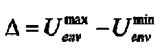
- U env max and U env min are previously determined highest and lowest values, respectively, of the voltage U env ( ⁇ ) of the waveform envelope of the potentials Pi ( ⁇ ) and Ni ( ⁇ ) from said selected family ( I,m ) of the potentials at the known value A o of the peak amplitude of said input analogue signals.
- the voltage interval ⁇ U env max - U env min , in which the voltage U env ( ⁇ ) of the waveform envelope of the potentials Pi ( ⁇ ) and Ni ( ⁇ ) from said selected family ( I ,1) of the potentials undulates, is narrow ( Fig. 3 ).
- a low waviness of the voltage U env ( ⁇ ) of the waveform envelope is that inherent feature of the known method, which according to the invention is exploited to improve the interpolation method.
- Said voltage value U measured any instant of time always falls in this narrow interval ⁇ and the actual peak amplitude A of the input analogue signals is for the factor k I,m above the voltage values falling within this narrow interval ⁇ . This feature is exploited for a simplified automatic gain control in the encoder.
- the factor k I,m is determined in one of the following three ways.
- the highest value U env max and the lowest value U env min of the voltage U nev ( ⁇ ) of the waveform envelope of the potentials Pi ( ⁇ ) and Ni ( ⁇ ) from the selected family ( I,m ) of the potentials at the known value A o of the peak amplitude of said input analogue signals may be calculated and the factor k I,m is calculated. Or there are previously measured the highest value U env max and the lowest value U env min of the voltage U env ( ⁇ ) of the waveform envelope of the potentials Pi ( ⁇ ) and Ni ( ⁇ ) from said selected family ( I,m ) of the potentials at the known value A o of the peak amplitude of said input analogue signals and the factor k I,m is calculated.
- the actual peak amplitude A is determined with the relative accuracy of ⁇ 0,029 .
- said voltage U is conducted directly to the input of an automatic gain control circuit, whereat the input voltage of this circuit is already set to U env max + U env min 2 1 ⁇ 1 2 ⁇ ⁇ A o .
- the invention also relates to an improvement of the interpolation circuit provided for a high-resolution encoder.
- the interpolation analogue-to-digital converter iadc comprises a first resistor chain of a first resistor r1, a second resistor r2 and so on up to an I -th resistor rI, which are series-connected to each other, and a second resistor chain of a first (dash) resistor r'1, a second (dash) resistor r'2 and so on up to an I -th (dash) resistor r'I, which are series-connected to each other.
- the first input analogue signal A + ( ⁇ ) is conducted to a first terminal of the first resistor r1 at the beginning of the first resistor chain and the third input analogue signal A - ( ⁇ ) is conducted to a second terminal of the I -th resistor rI at the end of the first resistor chain and the third input analogue signal A - ( ⁇ ) is conducted to a first terminal of the first resistor r'1 at the beginning of the second resistor chain and the first input analogue signal A + ( ⁇ ) is conducted to a second terminal of the I -th resistor r'I at the end of the second resistor chain and the fourth input analogue signal B - ( ⁇ ) is conducted to a second terminal of the I 2 - th resistor r ⁇ I 2 in the first resistor chain and the second input analogue signal B + ( ⁇ ) is conducted to a second terminal of the I 2 - th resistor r ⁇ ⁇ I 2 in the second resistor chain.
- the first input analogue signal A + ( ⁇ ), the second input analogue signal B + ( ⁇ ) , the third input analogue signal A - ( ⁇ ) and the fourth input analogue signal B - ( ⁇ ) are each time mutually in quadrature.
- the functional dependence of the first input analogue signal A + ( ⁇ ) on the observed argument a is sin ⁇ .
- the inputs of a first comparator c1 from whose outputs the first intermediate digital signal F 1( ⁇ ) and the first inverted intermediate digital signal G 1( ⁇ ) are taped, are connected to a first connection point cp1 on a second terminal of the first resistor r1 in the first resistor chain and to a first (dash) connection point cp'1 on a second terminal of the first (dash) resistor r'1 in the second resistor chain, respectively.
- each intermediate digital signal Fi ( ⁇ ) results from a comparison of the potential Pi ( ⁇ ) of the first input analogue signal A + ( ⁇ ) at the value ⁇ + ⁇ i of the observed argument ⁇ within the first half-period and with the amplitude reduced according to the resistance ratio of said resistors to the potential Ni ( ⁇ ), which is inverse to the potential Pi ( ⁇ ), of the third input analogue signal A- ( ⁇ ) at the same value ⁇ + ⁇ i of the observed argument ⁇ and with the amplitude reduced according to the resistance ratio of said resistors.
- the resistances of the two first resistors r1 and r'1, two second resistors r2 and r'2 and so on up to the two I -th resistors rI and r'I, which are each time equally situated in the respective first and second resistor chain, are determined so that the values ⁇ i are uniformly distributed within the first half-period of the observed argument ⁇ and that the potential P ( I /2)( ⁇ ) is equal to the signal B - ( ⁇ ) and the potential P ( I )( ⁇ ) equals to the signal A - ( ⁇ ) and the potential N ( I /2)( ⁇ ) equals the signal B + ( ⁇ ) and the potential N ( I )( ⁇ ) equals the signal A + ( ⁇ ) ( SI patent 21577 ).
- the invention improves the represented interpolation analogue-to-digital converter by means of a circuit pamc for measuring the peak amplitude of the input signals in the following way.
- the output of the first and second differential amplifiers da'i, da"i is connected to a gate terminal of a respective first and second follower transistors t'i, t"i.
- the sources of the follower transistors t'i, t"i are connected to a common sources terminal csi in the i -th local circuit lci.
- the common sources terminals csi of all local circuits lci are connected to a drain terminal of a common load transistor tcal and to a source of a diode-connected transistor tdc.
- a source of the common load transistor tcal is mass-connected.
- the drain of the diode-connected transistor tdc is connected to a current source transistor tcs, to an output of the interpolation analogue-to-digital converter iadc for the voltage U env ( ⁇ ) of the waveform envelope of the reference potentials Pi ( ⁇ ) and Ni ( ⁇ ) from the selected family ( I,m ) of the potentials and to an inverting input of the respective first and second differential amplifiers da'i, da"i pertaining to all said values of the index i .
- the transistors t'i, t"i, tcal, tdc, tcs must be NMOS transistors if the voltage U env ( ⁇ ) should represent the upper waveform envelope of the reference potentials Pi ( ⁇ ) and Ni ( ⁇ ).
- Said values of the index i at the selected interpolation number I are determined by means of that value of index m , at which the potentials Pi ( ⁇ ) and Ni ( ⁇ ), which belong to the selected family ( I,m ) of the potentials, have the waveform envelope with the voltage U env ( ⁇ ) having the lowest waviness.
- the improved interpolation circuit operates in the following way as far the determination of the actual peak amplitude of the input signals is concerned.
- the follower transistors t'i, t"i in the i -th local circuit lci constitute a local follower together with the transistor tcal representing their active load.
- the output voltage CS of the local follower is for the control voltage of the follower transistors t'i, t"i lower than the highest voltage of the reference potentials Pi ( ⁇ ) and Ni ( ⁇ ). Since the voltage U env ( ⁇ ) of the feedback should follow the voltages of the reference potentials Pi ( ⁇ ) and Ni ( ⁇ ) the outer follower is provided with the differential amplifiers da'i, da"i.
- the voltage CS must be raised for the control voltage of the follower transistors t'i, t"i. This is achieved in that the voltage of the diode-connected transistor tdc is added thereto.
- the voltage U env ( ⁇ ) in the feedback is compared to all reference potentials Pi ( ⁇ ) and Ni ( ⁇ ) in all local circuits lci.
- the voltage on the transistor tcal which is the common active load of all follower transistors t'i, t"i, follows the instantaneously highest voltage of the reference potentials Pi ( ⁇ ) and Ni ( ⁇ ) since the transistors are of NMOS type.
- the one of the follower transistors t'i, t"i which is controlled by the differential amplifier da'i, da"i having the voltage of one of the reference potentials Pi ( ⁇ ) and Ni ( ⁇ ) lower than the voltage U env ( ⁇ ) on its inverting input, namely closes. Therefore, the voltage U env ( ⁇ ) in the feedback, which is also the voltage at the output of the interpolation analogue-to-digital converter iadc, is the voltage U env ( ⁇ ) of the upper waveform envelope and the represented method as improved by the invention can be carried out by the circuit as improved according to the invention. But the function of the differential amplifiers da'i, da"i is also to raise the level of the input control signal of the follower transistors t'i, t"i and to lower the resistance of the local followers in the common sources terminal csi.
- the voltage U env ( ⁇ ) is also present at the output of the interpolation analogue-digital converter iadc when the measuring device is at rest and the sensors are not displaced with regard to the graduated scale.
- the automatic gain control in the measuring device can also be carried out when the displacement of the sensors with regard to the graduated scale is stopped and no measurement is performed.
- the improved method and circuit namely, do not depend on the frequency of the input signals, which may range from zero to several hundred kilohertz.
Landscapes
- Physics & Mathematics (AREA)
- General Physics & Mathematics (AREA)
- Analogue/Digital Conversion (AREA)
- Radar Systems Or Details Thereof (AREA)
Claims (12)
- Interpolationsverfahren mit einer Interpolationszahl I,
das in einem hochauflösenden Kodierer verwendbar ist und
dessen eingangsseitige Zustände durch ein erstes Eingangsanalogsignal A + (α), ein zweites Eingangsanalogsignal B + (α), ein drittes Eingangsanalogsignal A - (α) und ein viertes Eingangsanalogsignal B - (α) bestimmt sind, wobei die genannten Signale jeweils um die Viertelperiode zueinander verschoben sind,
wobei die funktionale Abhängigkeit des ersten Eingangsanalogsignals A + (α) von dem beobachteten Argument α als sin α darstellbar ist, und
das einen Interpolationsschritt umfasst,
in dem digitale Zwischensignale Fi(α) und invertierte digitale Zwischensignale Gi(α), i = 1,..I, gebildet werden,
indem jedes digitale Zwischensignal Fi(α) vom Vergleichen eines Potentials Pi(α) des ersten Eingangsanalogsignals A + (α) bei dem Wert α+αi seines beobachteten Argumentes α innerhalb einer ersten Halbperiode mit einem Potential Ni(α), das invers zum Potential Pi(α) ist, des dritten Eingangsanalogsignals A - (α) bei demselben Wert α+αi des beobachteten Argumentes α resultiert,
wobei die Werte αi des beobachteten Argumentes α gleichmässig innnerhalb der ersten Halbperiode verteilt sind und
das Potential P(I/2)(α) dem Signal B - (α), das Potential P(I)(α) dem Signal A - (α), das Potential N(I/2)(α) dem Signal B + (α) und das Potential N(I)(α) dem Signal A + (α) gleichen, und
einen Schritt eines logischen Kombinierens der genannten Zwischensignale Fi(α) und Gi(α),
um ein erstes Ausgangsdigitalsignal und
ein zweites, um die Viertelperiode dazu verschobenes Ausgangsdigitalsignal gebildet zu werden,
dadurch gekennzeichnet,
dass bei jeglichem Wert des beobachteten Arguments α ein Wert U jener Spannung der genannten Potentiale Pi(α) und Ni(α) zum Nullniveau gemessen wird,
die derzeit die höchste unter den Spannungen an Klemmen mit den genannten Potentialen Pi(α) and Ni(α) ist, die einer Familie (I,m) der Potentiale mit Indexwerten i=m,I/2-m,I/2+m,1-m gehören, wobei m einer positiven Ganzzahl im Interval von 1 bis I/2 -1 gleicht,
und dass eine tatsächliche grösste Amplitude A der Eingangsanalogsignale A + (α), B + (α), A - (α)and B - (α) als
bestimmt wird,
wobei der Faktor kI,m als
bestimmt wird und

- Interpolationsverfahren nach Anspruch 1, dadurch gekennzeichnet,
dass der höchste Wert

- Interpolationsverfahren nach Anspruch 1, dadurch gekennzeichnet,
dass der höchste Wert

- Interpolationsverfahren nach dem Anspruch 1, dadurch gekennzeichnet,
dass ein Wert Up der Spannung Uenv (α) der Wellenformeinhüllenden der Potentiale Pi(α) and Ni(α) aus der genannten ausgewählten Familie (I,m) der Potentiale zu einem Wert des beobachteten Arguments α zum bekannten Wert Ao der grössten Amplitude der genannten Eingangsanalogsignale vorher gemessen wird und der Faktor
errechnet wird. - Interpolationsverfahren nach Anspruch 2, 3 oder 4, dadurch gekennzeichnet, dass der Wert U der Spannung, die derzeit die höchste unter den Spannungen an Klemmen mit den genannten Potentialen Pi(α) und Ni(α) aus der ausgewählten Familie (I,m) der Potentiale ist, gemessen wird, wobei die Wellenformeinhüllende mit der Spannung Uenv (α) der Potenziale dieser Familie eine niedrigste Welligkeit

- Interpolationsverfahren nach Anspruch 5, dadurch gekennzeichnet,
dass die Potenziale der Familie (I,1) zum Messen des Wertes U verwendet werden. - Interpolationsverfahren nach einem der vorangehenden Ansprüche, dadurch gekennzeichnet,
dass die Interpolationszahl I = 8 ist. - Interpolationsschaltung mit einer Interpolationszahl I,
die in einem hochauflösenden Kodierer verwendbar ist und
in der ein erstes Ausgangsdigitalsignal und ein zweites, um die Viertelperiode dazu verschobenes Ausgangsdigitalsignal durch logisches Kombinieren digitaler Zwischensignale Fi(α) und invertierter digitaler Zwischensignale Gi(α), i=1,..I,
gebildet werden,
die in einem Interpolations-Analog-Digital-Wandler (iadc) gebildet werden,
der eine erste Widerstandskette mit einem ersten Widerstand (r1), einem zweiten Widerstand (r2) und so weiter bis zu einem I-ten Widerstand (rI) umfasst,
die zueinander reihengeschaltet sind, und
der eine zweite Widerstandskette mit einem ersten-Strich Widerstand (r'1), einem zweiten-Strich Widerstand (r'2) und so weiter bis zu einem I-ten-Strich Widerstand (r'I) umfasst,
die zueinander reihengeschaltet sind, und
in dem in der ersten beziehungsweise zweiten Widerstandskette jeweils gleich gelegenen der erste und der erste-Strich Widerstand (r1, r'1), der zweite und der zweite-Strich Widerstand (r'2) und so weiter bis zu dem I-ten und dem I-ten-Strich Widerstand (rI, r'I) gleichen Widerstand haben, und
in dem ein erstes Eingangsanalogsignal A + (α) an eine erste Klemme des ersten Widerstandes (r1) am Anfang der ersten Widerstandskette geleitet wird und
ein drittes Eingangsanalogsignal A - (α) an eine zweite Klemme des I-ten Widerstandes (rI) am Ende der ersten Widerstandskette geleitet wird und
das dritte Eingangsanalogsignal A - (α) an eine erste Klemme des ersten-Strich Widerstandes (r'1) am Anfang der zweiten Widerstandskette geleitet wird und
das erste Eingangsanalogsignal A + (α) an eine zweite Klemme des I-ten-Strich Widerstandes (r'I) am Ende der zweiten Widerstandskette geleitet wird und
ein viertes Eingangsanalogsignal B - (α) an eine zweite Klemme des

ein zweites Eingangsanalogsignal B + (α) an eine zweite Klemme des

wobei das erste Eingangsanalogsignal A + (α), das zweite Eingangsanalogsignal B + (α), das dritte Eingangsanalogsignal A - (α) und das vierte Eingangsanalogsignal B - (α) jeweils um die Viertelperiode zueinander verschoben sind und
die funktionale Abhängigkeit des ersten Eingangsanalogsignals A + (α) von dem beobachteten Argurnent α als sin α darstellbar ist, und
in dem Eingänge eines ersten Komparators (c1),
von dessen Ausgängen das erste digitale Zwischensignal F1(α) und das erste invertierte Zwischensignal G1(α) abgegriffen werden,
an eine zweite Klemme des ersten Widerstandes (r1) in der ersten Widerstandskette beziehungsweise an eine zweite Klemme des ersten-Strich Widerstandes (r'1) in der zweiten Widerstandskette angeschlossen sind und
ein zweiter Komparator (c2), ein dritter Komparator (c3) und so weiter bis zu einem I-ten Komparator (cI) auf dieselbe Weise angeschlossen sind,
an deren Ausgang die weiteren digitalen Zwischensignale Fi(α) und invertierten digitalen Zwischensignale Gi(α) abgegriffen werden,
wobei jedes digitale Zwischensignal Fi(α) ein Ergebnis des Vergleichens des Potentials Pi(α) des ersten Eingangsanalogsignales A + (α) bei dem Wert α+αi seines beobachteten Argumentes α innerhalb der ersten Halbperiode und mit einer durch das Verhältnis der genanten Widerstände bestimmten Amplitude zum Potential Ni(α), das invers zum Potential Pi(α) ist, des dritten Eingangsanalogsignales A - (α) bei demselben Wert α+αi des beobachteten Argumentes α und mit einer durch das Verhältnis der genanten Widerstände bestimmten Amplitude ist, und
in dem die Widerstände des ersten und des ersten-Strich Widerstandes (r1, r'1), des zweiten und des zweiten-Strich Widerstandes (r2, r'2) und so weiter bis zum I-ten und the I-ten-Strich Widerstandes (rI, r'I), die jedesmal gleich in der bezüglichen ersten und zweiten Widerstandskette gelegen sind, so bestimmt werden,
dass die Werte αi innerhalb der ersten Halbperiode des beobachteten Arguments α gleichmässig verteilt sind und
das Potential P(I/2)(α) dem Signal B - (α) gleicht, das Potential P(I)(α) dem Signal A - (α) gleicht, das Potential N(I/2)(α) dem Signal B + (α) gleicht und das Potential N(I)(α) dem Signal A + (α) gleicht,
dadurch gekennzeichnet,
dass jedes Paar der Potentiale Fi(α) und Ni(α) mit den Werten i=m,I/2-m,I/2+m,I-m des Indizes, wobei m der Null oder einer positiven Ganzzahl im Bereich von 1 to I/2-1 gleicht, an einen nichtinvertierenden Eingang eines bezüglichen ersten oder zweiten Differentialverstärkers (da'i, da"i) zu diesem Index i geleitet wird,
dessen Ausgang an eine Gateklemme eines bezüglichen ersten oder zweiten Folgetransistors (t'i, t"i) angeschlossen ist,
deren Quellen an eine gemeinsame Quellenklemme (csi) angeschlossen sind,
und dass die genannten gemeinsamen Quellenklemmen (csi) für alle genannten Werte des Indizes i an eine Drainklemme eines Lasttransistors (tcal), dessen Quelle an Masse angeschlossen ist, und an eine Quelle eines diodenähnlich angeschlossenen Transistors (tdc) angeschlossen sind, dessen Drain an einen Stromquellentransistor (tcs), an einen Ausgang für die Spannung Uenv (α) der Wellenformeinhüllenden der Potentiale Pi(α) and Ni(α) aus der genanten ausgewählten Familie (I,m) der Potentiale und an einen invertierenden Eingang eines bezüglichen ersten oder zweiten Differentialverstärkers (da'i, da"i) für alle genannten Werte des Indizes i angeschlossen ist. - Interpolationsschaltung nach Anspruch 8, dadurch gekennzeichnet,
dass die genannten Werte des Indizes i bei der ausgewählten Interpolationszahl I mit Hilfe jenes Wertes vom Index m bestimmt werden, bei dem die Potentiale Pi(α) und
Ni(α) aus der ausgewählten Familie (I,m) der Potentiale die Wellenformeinhüllende mit der Spannung Uenv (α) mit der niedrigsten Welligkeit aufweisen. - Interpolationsschaltung nach Anspruch 9, dadurch gekennzeichnet,
dass die Werte 1,I/2-1,I/2+1,I-1 als die genannten Werte des Indizes i bei der ausgewählten Interpolationszahl I ausgewählt werden. - Interpolationsverfahren nach Anspruch 9, dadurch gekennzeichnet,
dass die Interpolationszahl I = 8 ist. - Interpolationsverfahren nach einem der Ansprüche 9 bis 11, dadurch gekennzeichnet,
dass die Transistoren (t'i, t"i, tcal, tdc, tcs) NMOS Transistoren sind.
Applications Claiming Priority (2)
| Application Number | Priority Date | Filing Date | Title |
|---|---|---|---|
| SI200600238A SI22397A (sl) | 2006-10-11 | 2006-10-11 | Interpolacijski postopek in vezje za izvajanje tega postopka, ki se uporabljata za kodirnik z visoko locljivostjo |
| PCT/SI2007/000017 WO2008045005A1 (en) | 2006-10-11 | 2007-03-28 | Interpolation method and a circuit for carrying out said method used in a high-resolution encoder |
Publications (2)
| Publication Number | Publication Date |
|---|---|
| EP2079988A1 EP2079988A1 (de) | 2009-07-22 |
| EP2079988B1 true EP2079988B1 (de) | 2010-07-07 |
Family
ID=38544004
Family Applications (1)
| Application Number | Title | Priority Date | Filing Date |
|---|---|---|---|
| EP07716178A Not-in-force EP2079988B1 (de) | 2006-10-11 | 2007-03-28 | Interpolationsverfahren und schaltung zum ausführen des verfahrens zur verwendung in einem hochauflösenden kodierer |
Country Status (6)
| Country | Link |
|---|---|
| US (1) | US7777661B2 (de) |
| EP (1) | EP2079988B1 (de) |
| AT (1) | ATE473422T1 (de) |
| DE (1) | DE602007007649D1 (de) |
| SI (1) | SI22397A (de) |
| WO (1) | WO2008045005A1 (de) |
Families Citing this family (2)
| Publication number | Priority date | Publication date | Assignee | Title |
|---|---|---|---|---|
| US8797966B2 (en) | 2011-09-23 | 2014-08-05 | Ofinno Technologies, Llc | Channel state information transmission |
| US8848673B2 (en) | 2011-12-19 | 2014-09-30 | Ofinno Technologies, Llc | Beam information exchange between base stations |
Family Cites Families (9)
| Publication number | Priority date | Publication date | Assignee | Title |
|---|---|---|---|---|
| DE1945206C3 (de) * | 1969-09-06 | 1974-02-21 | Fa. Carl Zeiss, 7920 Heidenheim | Einrichtung zur Interpolation |
| DE3686705T2 (de) * | 1985-12-16 | 1993-04-01 | Philips Nv | Schaltung zur interpolation zwischen komplementaeren spannungen. |
| JPS6312915A (ja) | 1986-07-03 | 1988-01-20 | Yamaha Corp | エンコ−ダ用検出信号処理回路 |
| US5805096A (en) * | 1995-05-31 | 1998-09-08 | U.S. Philips Corporation | A/D converter with interpolation |
| US6375238B1 (en) * | 1999-03-24 | 2002-04-23 | Anthony Hopkins | Rail-hanging package facing device |
| DE10301848B4 (de) * | 2003-01-09 | 2014-10-09 | Anton Rodi | Messeinrichtung zur Erfassung von Größen, insbesondere von Winkeln oder Wegstrecken |
| SI21577A (sl) * | 2003-07-02 | 2005-02-28 | Anton PLETERŠEK | Interpolacijski postopek in interpolacijsko vezje, ki se uporabljata za kodirnik z visoko ločljivostjo |
| EP1770866B1 (de) * | 2005-09-12 | 2008-04-02 | Rohde & Schwarz GmbH & Co. KG | Schneller Analog-Digital-Wandler |
| SI22403A (sl) | 2006-09-21 | 2008-04-30 | Anton Pletersek | Postopek za samodejno reguliranje amplitude vhodnih signalov |
-
2006
- 2006-10-11 SI SI200600238A patent/SI22397A/sl not_active IP Right Cessation
-
2007
- 2007-03-28 EP EP07716178A patent/EP2079988B1/de not_active Not-in-force
- 2007-03-28 US US12/311,655 patent/US7777661B2/en active Active
- 2007-03-28 WO PCT/SI2007/000017 patent/WO2008045005A1/en not_active Ceased
- 2007-03-28 AT AT07716178T patent/ATE473422T1/de not_active IP Right Cessation
- 2007-03-28 DE DE602007007649T patent/DE602007007649D1/de active Active
Also Published As
| Publication number | Publication date |
|---|---|
| WO2008045005A1 (en) | 2008-04-17 |
| DE602007007649D1 (de) | 2010-08-19 |
| SI22397A (sl) | 2008-04-30 |
| ATE473422T1 (de) | 2010-07-15 |
| EP2079988A1 (de) | 2009-07-22 |
| US7777661B2 (en) | 2010-08-17 |
| US20100019942A1 (en) | 2010-01-28 |
Similar Documents
| Publication | Publication Date | Title |
|---|---|---|
| CN101131329A (zh) | 编码器信号的校正电路 | |
| US9634681B1 (en) | Analog-to-digital conversion with linearity calibration | |
| CN101140170A (zh) | 编码器信号的校正电路 | |
| US7777661B2 (en) | Interpolation method and a circuit for carrying out said method used in a high-resolution encoder | |
| US7460979B2 (en) | Method and system for enhanced resolution, automatically-calibrated position sensor | |
| US20150112634A1 (en) | Angle detection device and angle detection method | |
| US20150333762A1 (en) | Method For Linearization Of The Output Of An Analog-To-Digital Converter And Measuring Instruments Using Such Method | |
| JP2004333156A (ja) | エンコーダ信号内挿分割器 | |
| US7042373B2 (en) | Error measuring method for digitally self-calibrating pipeline ADC and apparatus thereof | |
| Jovanović et al. | An improved linearization circuit used for optical rotary encoders | |
| JP5162739B2 (ja) | エンコーダ信号処理方法、エンコーダ装置及びサーボモータ | |
| US20020175688A1 (en) | Method and an apparatus for measuring the ratio of the amplification factor of a signal level normalizer | |
| US7197413B2 (en) | Delay amount measurement method | |
| JP3678066B2 (ja) | インクリメンタル型エンコーダ | |
| CN106856397B (zh) | 振幅校正电路及其应用的信号校正电路 | |
| JPH0658769A (ja) | 信号処理方法及びそれを用いた変位検出装置 | |
| JPH0522182B2 (de) | ||
| US20030163265A1 (en) | DSP assisted peak capture circuit and method | |
| JPH0658772A (ja) | エンコーダ信号処理回路 | |
| NO761839L (de) | ||
| JP3782861B2 (ja) | A/d変換器の試験方法及びその試験装置 | |
| Ben-Brahim et al. | A new angle determination method for resolvers | |
| KR200360584Y1 (ko) | 디지털 측정장치 | |
| JPH01253673A (ja) | 波形測定装置 | |
| CN115800929A (zh) | 一种正交信号生成装置 |
Legal Events
| Date | Code | Title | Description |
|---|---|---|---|
| PUAI | Public reference made under article 153(3) epc to a published international application that has entered the european phase |
Free format text: ORIGINAL CODE: 0009012 |
|
| 17P | Request for examination filed |
Effective date: 20090327 |
|
| AK | Designated contracting states |
Kind code of ref document: A1 Designated state(s): AT BE BG CH CY CZ DE DK EE ES FI FR GB GR HU IE IS IT LI LT LU LV MC MT NL PL PT RO SE SI SK TR |
|
| GRAP | Despatch of communication of intention to grant a patent |
Free format text: ORIGINAL CODE: EPIDOSNIGR1 |
|
| GRAS | Grant fee paid |
Free format text: ORIGINAL CODE: EPIDOSNIGR3 |
|
| GRAA | (expected) grant |
Free format text: ORIGINAL CODE: 0009210 |
|
| AK | Designated contracting states |
Kind code of ref document: B1 Designated state(s): AT BE BG CH CY CZ DE DK EE ES FI FR GB GR HU IE IS IT LI LT LU LV MC MT NL PL PT RO SE SI SK TR |
|
| REG | Reference to a national code |
Ref country code: GB Ref legal event code: FG4D |
|
| REG | Reference to a national code |
Ref country code: CH Ref legal event code: EP |
|
| REG | Reference to a national code |
Ref country code: IE Ref legal event code: FG4D |
|
| REF | Corresponds to: |
Ref document number: 602007007649 Country of ref document: DE Date of ref document: 20100819 Kind code of ref document: P |
|
| REG | Reference to a national code |
Ref country code: NL Ref legal event code: VDEP Effective date: 20100707 |
|
| PG25 | Lapsed in a contracting state [announced via postgrant information from national office to epo] |
Ref country code: SI Free format text: LAPSE BECAUSE OF FAILURE TO SUBMIT A TRANSLATION OF THE DESCRIPTION OR TO PAY THE FEE WITHIN THE PRESCRIBED TIME-LIMIT Effective date: 20100707 |
|
| LTIE | Lt: invalidation of european patent or patent extension |
Effective date: 20100707 |
|
| PG25 | Lapsed in a contracting state [announced via postgrant information from national office to epo] |
Ref country code: LT Free format text: LAPSE BECAUSE OF FAILURE TO SUBMIT A TRANSLATION OF THE DESCRIPTION OR TO PAY THE FEE WITHIN THE PRESCRIBED TIME-LIMIT Effective date: 20100707 Ref country code: FI Free format text: LAPSE BECAUSE OF FAILURE TO SUBMIT A TRANSLATION OF THE DESCRIPTION OR TO PAY THE FEE WITHIN THE PRESCRIBED TIME-LIMIT Effective date: 20100707 Ref country code: AT Free format text: LAPSE BECAUSE OF FAILURE TO SUBMIT A TRANSLATION OF THE DESCRIPTION OR TO PAY THE FEE WITHIN THE PRESCRIBED TIME-LIMIT Effective date: 20100707 Ref country code: NL Free format text: LAPSE BECAUSE OF FAILURE TO SUBMIT A TRANSLATION OF THE DESCRIPTION OR TO PAY THE FEE WITHIN THE PRESCRIBED TIME-LIMIT Effective date: 20100707 |
|
| PG25 | Lapsed in a contracting state [announced via postgrant information from national office to epo] |
Ref country code: PT Free format text: LAPSE BECAUSE OF FAILURE TO SUBMIT A TRANSLATION OF THE DESCRIPTION OR TO PAY THE FEE WITHIN THE PRESCRIBED TIME-LIMIT Effective date: 20101108 Ref country code: CY Free format text: LAPSE BECAUSE OF FAILURE TO SUBMIT A TRANSLATION OF THE DESCRIPTION OR TO PAY THE FEE WITHIN THE PRESCRIBED TIME-LIMIT Effective date: 20100707 Ref country code: BG Free format text: LAPSE BECAUSE OF FAILURE TO SUBMIT A TRANSLATION OF THE DESCRIPTION OR TO PAY THE FEE WITHIN THE PRESCRIBED TIME-LIMIT Effective date: 20101007 Ref country code: PL Free format text: LAPSE BECAUSE OF FAILURE TO SUBMIT A TRANSLATION OF THE DESCRIPTION OR TO PAY THE FEE WITHIN THE PRESCRIBED TIME-LIMIT Effective date: 20100707 Ref country code: IS Free format text: LAPSE BECAUSE OF FAILURE TO SUBMIT A TRANSLATION OF THE DESCRIPTION OR TO PAY THE FEE WITHIN THE PRESCRIBED TIME-LIMIT Effective date: 20101107 |
|
| PG25 | Lapsed in a contracting state [announced via postgrant information from national office to epo] |
Ref country code: SE Free format text: LAPSE BECAUSE OF FAILURE TO SUBMIT A TRANSLATION OF THE DESCRIPTION OR TO PAY THE FEE WITHIN THE PRESCRIBED TIME-LIMIT Effective date: 20100707 Ref country code: GR Free format text: LAPSE BECAUSE OF FAILURE TO SUBMIT A TRANSLATION OF THE DESCRIPTION OR TO PAY THE FEE WITHIN THE PRESCRIBED TIME-LIMIT Effective date: 20101008 Ref country code: BE Free format text: LAPSE BECAUSE OF FAILURE TO SUBMIT A TRANSLATION OF THE DESCRIPTION OR TO PAY THE FEE WITHIN THE PRESCRIBED TIME-LIMIT Effective date: 20100707 Ref country code: LV Free format text: LAPSE BECAUSE OF FAILURE TO SUBMIT A TRANSLATION OF THE DESCRIPTION OR TO PAY THE FEE WITHIN THE PRESCRIBED TIME-LIMIT Effective date: 20100707 |
|
| PG25 | Lapsed in a contracting state [announced via postgrant information from national office to epo] |
Ref country code: DK Free format text: LAPSE BECAUSE OF FAILURE TO SUBMIT A TRANSLATION OF THE DESCRIPTION OR TO PAY THE FEE WITHIN THE PRESCRIBED TIME-LIMIT Effective date: 20100707 |
|
| PLBE | No opposition filed within time limit |
Free format text: ORIGINAL CODE: 0009261 |
|
| STAA | Information on the status of an ep patent application or granted ep patent |
Free format text: STATUS: NO OPPOSITION FILED WITHIN TIME LIMIT |
|
| PG25 | Lapsed in a contracting state [announced via postgrant information from national office to epo] |
Ref country code: RO Free format text: LAPSE BECAUSE OF FAILURE TO SUBMIT A TRANSLATION OF THE DESCRIPTION OR TO PAY THE FEE WITHIN THE PRESCRIBED TIME-LIMIT Effective date: 20100707 Ref country code: IT Free format text: LAPSE BECAUSE OF FAILURE TO SUBMIT A TRANSLATION OF THE DESCRIPTION OR TO PAY THE FEE WITHIN THE PRESCRIBED TIME-LIMIT Effective date: 20100707 Ref country code: SK Free format text: LAPSE BECAUSE OF FAILURE TO SUBMIT A TRANSLATION OF THE DESCRIPTION OR TO PAY THE FEE WITHIN THE PRESCRIBED TIME-LIMIT Effective date: 20100707 Ref country code: CZ Free format text: LAPSE BECAUSE OF FAILURE TO SUBMIT A TRANSLATION OF THE DESCRIPTION OR TO PAY THE FEE WITHIN THE PRESCRIBED TIME-LIMIT Effective date: 20100707 Ref country code: EE Free format text: LAPSE BECAUSE OF FAILURE TO SUBMIT A TRANSLATION OF THE DESCRIPTION OR TO PAY THE FEE WITHIN THE PRESCRIBED TIME-LIMIT Effective date: 20100707 |
|
| 26N | No opposition filed |
Effective date: 20110408 |
|
| PG25 | Lapsed in a contracting state [announced via postgrant information from national office to epo] |
Ref country code: ES Free format text: LAPSE BECAUSE OF FAILURE TO SUBMIT A TRANSLATION OF THE DESCRIPTION OR TO PAY THE FEE WITHIN THE PRESCRIBED TIME-LIMIT Effective date: 20101018 |
|
| REG | Reference to a national code |
Ref country code: DE Ref legal event code: R097 Ref document number: 602007007649 Country of ref document: DE Effective date: 20110408 |
|
| PG25 | Lapsed in a contracting state [announced via postgrant information from national office to epo] |
Ref country code: MC Free format text: LAPSE BECAUSE OF NON-PAYMENT OF DUE FEES Effective date: 20110331 |
|
| REG | Reference to a national code |
Ref country code: CH Ref legal event code: PL |
|
| PG25 | Lapsed in a contracting state [announced via postgrant information from national office to epo] |
Ref country code: MT Free format text: LAPSE BECAUSE OF FAILURE TO SUBMIT A TRANSLATION OF THE DESCRIPTION OR TO PAY THE FEE WITHIN THE PRESCRIBED TIME-LIMIT Effective date: 20100707 |
|
| REG | Reference to a national code |
Ref country code: IE Ref legal event code: MM4A |
|
| PG25 | Lapsed in a contracting state [announced via postgrant information from national office to epo] |
Ref country code: IE Free format text: LAPSE BECAUSE OF NON-PAYMENT OF DUE FEES Effective date: 20110328 Ref country code: CH Free format text: LAPSE BECAUSE OF NON-PAYMENT OF DUE FEES Effective date: 20110331 Ref country code: LI Free format text: LAPSE BECAUSE OF NON-PAYMENT OF DUE FEES Effective date: 20110331 |
|
| REG | Reference to a national code |
Ref country code: GB Ref legal event code: 732E Free format text: REGISTERED BETWEEN 20130314 AND 20130320 |
|
| REG | Reference to a national code |
Ref country code: FR Ref legal event code: TP Owner name: IDS MICROCHIP AG, CH Effective date: 20130321 |
|
| PGFP | Annual fee paid to national office [announced via postgrant information from national office to epo] |
Ref country code: GB Payment date: 20130318 Year of fee payment: 7 Ref country code: FR Payment date: 20130329 Year of fee payment: 7 |
|
| PG25 | Lapsed in a contracting state [announced via postgrant information from national office to epo] |
Ref country code: LU Free format text: LAPSE BECAUSE OF NON-PAYMENT OF DUE FEES Effective date: 20110328 |
|
| REG | Reference to a national code |
Ref country code: DE Ref legal event code: R081 Ref document number: 602007007649 Country of ref document: DE Owner name: IDS MICROCHIP AG, CH Free format text: FORMER OWNER: PLETERSEK, ANTON, OREHOVA VAS, SI Effective date: 20130508 Ref country code: DE Ref legal event code: R081 Ref document number: 602007007649 Country of ref document: DE Owner name: AMS INTERNATIONAL AG, CH Free format text: FORMER OWNER: PLETERSEK, ANTON, OREHOVA VAS, SI Effective date: 20130508 |
|
| PG25 | Lapsed in a contracting state [announced via postgrant information from national office to epo] |
Ref country code: TR Free format text: LAPSE BECAUSE OF FAILURE TO SUBMIT A TRANSLATION OF THE DESCRIPTION OR TO PAY THE FEE WITHIN THE PRESCRIBED TIME-LIMIT Effective date: 20100707 |
|
| PG25 | Lapsed in a contracting state [announced via postgrant information from national office to epo] |
Ref country code: HU Free format text: LAPSE BECAUSE OF FAILURE TO SUBMIT A TRANSLATION OF THE DESCRIPTION OR TO PAY THE FEE WITHIN THE PRESCRIBED TIME-LIMIT Effective date: 20100707 |
|
| GBPC | Gb: european patent ceased through non-payment of renewal fee |
Effective date: 20140328 |
|
| REG | Reference to a national code |
Ref country code: FR Ref legal event code: ST Effective date: 20141128 |
|
| PG25 | Lapsed in a contracting state [announced via postgrant information from national office to epo] |
Ref country code: FR Free format text: LAPSE BECAUSE OF NON-PAYMENT OF DUE FEES Effective date: 20140331 Ref country code: GB Free format text: LAPSE BECAUSE OF NON-PAYMENT OF DUE FEES Effective date: 20140328 |
|
| REG | Reference to a national code |
Ref country code: DE Ref legal event code: R082 Ref document number: 602007007649 Country of ref document: DE Representative=s name: EPPING HERMANN FISCHER, PATENTANWALTSGESELLSCH, DE Ref country code: DE Ref legal event code: R081 Ref document number: 602007007649 Country of ref document: DE Owner name: AMS INTERNATIONAL AG, CH Free format text: FORMER OWNER: IDS MICROCHIP AG, WOLLERAU, CH Ref country code: DE Ref legal event code: R082 Ref document number: 602007007649 Country of ref document: DE Representative=s name: EPPING HERMANN FISCHER PATENTANWALTSGESELLSCHA, DE |
|
| P01 | Opt-out of the competence of the unified patent court (upc) registered |
Effective date: 20230821 |
|
| PGFP | Annual fee paid to national office [announced via postgrant information from national office to epo] |
Ref country code: DE Payment date: 20240320 Year of fee payment: 18 |
|
| REG | Reference to a national code |
Ref country code: DE Ref legal event code: R119 Ref document number: 602007007649 Country of ref document: DE |
|
| PG25 | Lapsed in a contracting state [announced via postgrant information from national office to epo] |
Ref country code: DE Free format text: LAPSE BECAUSE OF NON-PAYMENT OF DUE FEES Effective date: 20251001 |