EP2088577A2 - Dispositif électro-optique, procédé de commande de celui-ci, et appareil électronique - Google Patents
Dispositif électro-optique, procédé de commande de celui-ci, et appareil électronique Download PDFInfo
- Publication number
- EP2088577A2 EP2088577A2 EP09001504A EP09001504A EP2088577A2 EP 2088577 A2 EP2088577 A2 EP 2088577A2 EP 09001504 A EP09001504 A EP 09001504A EP 09001504 A EP09001504 A EP 09001504A EP 2088577 A2 EP2088577 A2 EP 2088577A2
- Authority
- EP
- European Patent Office
- Prior art keywords
- data
- electro
- period
- unit
- line
- Prior art date
- Legal status (The legal status is an assumption and is not a legal conclusion. Google has not performed a legal analysis and makes no representation as to the accuracy of the status listed.)
- Withdrawn
Links
- 238000000034 method Methods 0.000 title claims description 13
- 239000003990 capacitor Substances 0.000 claims abstract description 162
- 230000003287 optical effect Effects 0.000 claims description 3
- 239000010410 layer Substances 0.000 description 118
- 239000004065 semiconductor Substances 0.000 description 34
- 238000010586 diagram Methods 0.000 description 22
- 239000000463 material Substances 0.000 description 18
- 238000004519 manufacturing process Methods 0.000 description 14
- 238000005192 partition Methods 0.000 description 10
- 230000008901 benefit Effects 0.000 description 8
- 239000000758 substrate Substances 0.000 description 6
- 230000003071 parasitic effect Effects 0.000 description 5
- 229910052782 aluminium Inorganic materials 0.000 description 4
- XAGFODPZIPBFFR-UHFFFAOYSA-N aluminium Chemical compound [Al] XAGFODPZIPBFFR-UHFFFAOYSA-N 0.000 description 4
- 230000007423 decrease Effects 0.000 description 4
- 239000010408 film Substances 0.000 description 4
- 230000001413 cellular effect Effects 0.000 description 3
- 230000000052 comparative effect Effects 0.000 description 3
- 239000006185 dispersion Substances 0.000 description 3
- 230000002093 peripheral effect Effects 0.000 description 3
- 229910052710 silicon Inorganic materials 0.000 description 3
- 239000010703 silicon Substances 0.000 description 3
- 229910052709 silver Inorganic materials 0.000 description 3
- 239000010409 thin film Substances 0.000 description 3
- 230000000903 blocking effect Effects 0.000 description 2
- 230000003247 decreasing effect Effects 0.000 description 2
- 230000012447 hatching Effects 0.000 description 2
- AMGQUBHHOARCQH-UHFFFAOYSA-N indium;oxotin Chemical compound [In].[Sn]=O AMGQUBHHOARCQH-UHFFFAOYSA-N 0.000 description 2
- 229910052749 magnesium Inorganic materials 0.000 description 2
- 239000011777 magnesium Substances 0.000 description 2
- 229910052751 metal Inorganic materials 0.000 description 2
- 239000002184 metal Substances 0.000 description 2
- 238000000059 patterning Methods 0.000 description 2
- 230000008569 process Effects 0.000 description 2
- 239000004332 silver Substances 0.000 description 2
- 238000009751 slip forming Methods 0.000 description 2
- YVTHLONGBIQYBO-UHFFFAOYSA-N zinc indium(3+) oxygen(2-) Chemical compound [O--].[Zn++].[In+3] YVTHLONGBIQYBO-UHFFFAOYSA-N 0.000 description 2
- 229910000967 As alloy Inorganic materials 0.000 description 1
- OYPRJOBELJOOCE-UHFFFAOYSA-N Calcium Chemical compound [Ca] OYPRJOBELJOOCE-UHFFFAOYSA-N 0.000 description 1
- FYYHWMGAXLPEAU-UHFFFAOYSA-N Magnesium Chemical compound [Mg] FYYHWMGAXLPEAU-UHFFFAOYSA-N 0.000 description 1
- 239000000783 alginic acid Substances 0.000 description 1
- 229910045601 alloy Inorganic materials 0.000 description 1
- 239000000956 alloy Substances 0.000 description 1
- 239000011668 ascorbic acid Substances 0.000 description 1
- 229910052791 calcium Inorganic materials 0.000 description 1
- 239000011575 calcium Substances 0.000 description 1
- 239000004020 conductor Substances 0.000 description 1
- 230000005525 hole transport Effects 0.000 description 1
- 238000003475 lamination Methods 0.000 description 1
- 239000011159 matrix material Substances 0.000 description 1
- 239000007769 metal material Substances 0.000 description 1
- 230000004048 modification Effects 0.000 description 1
- 238000012986 modification Methods 0.000 description 1
- 238000001579 optical reflectometry Methods 0.000 description 1
- 229920000642 polymer Polymers 0.000 description 1
- 230000001737 promoting effect Effects 0.000 description 1
- 230000009467 reduction Effects 0.000 description 1
- 239000002356 single layer Substances 0.000 description 1
- 230000003068 static effect Effects 0.000 description 1
- 230000007704 transition Effects 0.000 description 1
Images


Classifications
-
- G—PHYSICS
- G09—EDUCATION; CRYPTOGRAPHY; DISPLAY; ADVERTISING; SEALS
- G09G—ARRANGEMENTS OR CIRCUITS FOR CONTROL OF INDICATING DEVICES USING STATIC MEANS TO PRESENT VARIABLE INFORMATION
- G09G3/00—Control arrangements or circuits, of interest only in connection with visual indicators other than cathode-ray tubes
- G09G3/20—Control arrangements or circuits, of interest only in connection with visual indicators other than cathode-ray tubes for presentation of an assembly of a number of characters, e.g. a page, by composing the assembly by combination of individual elements arranged in a matrix no fixed position being assigned to or needed to be assigned to the individual characters or partial characters
- G09G3/22—Control arrangements or circuits, of interest only in connection with visual indicators other than cathode-ray tubes for presentation of an assembly of a number of characters, e.g. a page, by composing the assembly by combination of individual elements arranged in a matrix no fixed position being assigned to or needed to be assigned to the individual characters or partial characters using controlled light sources
- G09G3/30—Control arrangements or circuits, of interest only in connection with visual indicators other than cathode-ray tubes for presentation of an assembly of a number of characters, e.g. a page, by composing the assembly by combination of individual elements arranged in a matrix no fixed position being assigned to or needed to be assigned to the individual characters or partial characters using controlled light sources using electroluminescent panels
- G09G3/32—Control arrangements or circuits, of interest only in connection with visual indicators other than cathode-ray tubes for presentation of an assembly of a number of characters, e.g. a page, by composing the assembly by combination of individual elements arranged in a matrix no fixed position being assigned to or needed to be assigned to the individual characters or partial characters using controlled light sources using electroluminescent panels semiconductive, e.g. using light-emitting diodes [LED]
- G09G3/3208—Control arrangements or circuits, of interest only in connection with visual indicators other than cathode-ray tubes for presentation of an assembly of a number of characters, e.g. a page, by composing the assembly by combination of individual elements arranged in a matrix no fixed position being assigned to or needed to be assigned to the individual characters or partial characters using controlled light sources using electroluminescent panels semiconductive, e.g. using light-emitting diodes [LED] organic, e.g. using organic light-emitting diodes [OLED]
- G09G3/3225—Control arrangements or circuits, of interest only in connection with visual indicators other than cathode-ray tubes for presentation of an assembly of a number of characters, e.g. a page, by composing the assembly by combination of individual elements arranged in a matrix no fixed position being assigned to or needed to be assigned to the individual characters or partial characters using controlled light sources using electroluminescent panels semiconductive, e.g. using light-emitting diodes [LED] organic, e.g. using organic light-emitting diodes [OLED] using an active matrix
- G09G3/3258—Control arrangements or circuits, of interest only in connection with visual indicators other than cathode-ray tubes for presentation of an assembly of a number of characters, e.g. a page, by composing the assembly by combination of individual elements arranged in a matrix no fixed position being assigned to or needed to be assigned to the individual characters or partial characters using controlled light sources using electroluminescent panels semiconductive, e.g. using light-emitting diodes [LED] organic, e.g. using organic light-emitting diodes [OLED] using an active matrix with pixel circuitry controlling the voltage across the light-emitting element
-
- H—ELECTRICITY
- H10—SEMICONDUCTOR DEVICES; ELECTRIC SOLID-STATE DEVICES NOT OTHERWISE PROVIDED FOR
- H10D—INORGANIC ELECTRIC SEMICONDUCTOR DEVICES
- H10D84/00—Integrated devices formed in or on semiconductor substrates that comprise only semiconducting layers, e.g. on Si wafers or on GaAs-on-Si wafers
- H10D84/90—Masterslice integrated circuits
- H10D84/903—Masterslice integrated circuits comprising field effect technology
- H10D84/907—CMOS gate arrays
- H10D84/968—Macro-architecture
- H10D84/974—Layout specifications, i.e. inner core regions
- H10D84/979—Data lines, e.g. buses
-
- H—ELECTRICITY
- H10—SEMICONDUCTOR DEVICES; ELECTRIC SOLID-STATE DEVICES NOT OTHERWISE PROVIDED FOR
- H10K—ORGANIC ELECTRIC SOLID-STATE DEVICES
- H10K59/00—Integrated devices, or assemblies of multiple devices, comprising at least one organic light-emitting element covered by group H10K50/00
- H10K59/10—OLED displays
- H10K59/12—Active-matrix OLED [AMOLED] displays
- H10K59/121—Active-matrix OLED [AMOLED] displays characterised by the geometry or disposition of pixel elements
- H10K59/1213—Active-matrix OLED [AMOLED] displays characterised by the geometry or disposition of pixel elements the pixel elements being TFTs
-
- H—ELECTRICITY
- H10—SEMICONDUCTOR DEVICES; ELECTRIC SOLID-STATE DEVICES NOT OTHERWISE PROVIDED FOR
- H10K—ORGANIC ELECTRIC SOLID-STATE DEVICES
- H10K59/00—Integrated devices, or assemblies of multiple devices, comprising at least one organic light-emitting element covered by group H10K50/00
- H10K59/10—OLED displays
- H10K59/12—Active-matrix OLED [AMOLED] displays
- H10K59/121—Active-matrix OLED [AMOLED] displays characterised by the geometry or disposition of pixel elements
- H10K59/1216—Active-matrix OLED [AMOLED] displays characterised by the geometry or disposition of pixel elements the pixel elements being capacitors
-
- G—PHYSICS
- G09—EDUCATION; CRYPTOGRAPHY; DISPLAY; ADVERTISING; SEALS
- G09G—ARRANGEMENTS OR CIRCUITS FOR CONTROL OF INDICATING DEVICES USING STATIC MEANS TO PRESENT VARIABLE INFORMATION
- G09G2300/00—Aspects of the constitution of display devices
- G09G2300/04—Structural and physical details of display devices
- G09G2300/0421—Structural details of the set of electrodes
- G09G2300/0426—Layout of electrodes and connections
-
- G—PHYSICS
- G09—EDUCATION; CRYPTOGRAPHY; DISPLAY; ADVERTISING; SEALS
- G09G—ARRANGEMENTS OR CIRCUITS FOR CONTROL OF INDICATING DEVICES USING STATIC MEANS TO PRESENT VARIABLE INFORMATION
- G09G2300/00—Aspects of the constitution of display devices
- G09G2300/04—Structural and physical details of display devices
- G09G2300/0439—Pixel structures
- G09G2300/0465—Improved aperture ratio, e.g. by size reduction of the pixel circuit, e.g. for improving the pixel density or the maximum displayable luminance or brightness
-
- G—PHYSICS
- G09—EDUCATION; CRYPTOGRAPHY; DISPLAY; ADVERTISING; SEALS
- G09G—ARRANGEMENTS OR CIRCUITS FOR CONTROL OF INDICATING DEVICES USING STATIC MEANS TO PRESENT VARIABLE INFORMATION
- G09G2300/00—Aspects of the constitution of display devices
- G09G2300/08—Active matrix structure, i.e. with use of active elements, inclusive of non-linear two terminal elements, in the pixels together with light emitting or modulating elements
-
- G—PHYSICS
- G09—EDUCATION; CRYPTOGRAPHY; DISPLAY; ADVERTISING; SEALS
- G09G—ARRANGEMENTS OR CIRCUITS FOR CONTROL OF INDICATING DEVICES USING STATIC MEANS TO PRESENT VARIABLE INFORMATION
- G09G2330/00—Aspects of power supply; Aspects of display protection and defect management
- G09G2330/02—Details of power systems and of start or stop of display operation
- G09G2330/021—Power management, e.g. power saving
-
- G—PHYSICS
- G09—EDUCATION; CRYPTOGRAPHY; DISPLAY; ADVERTISING; SEALS
- G09G—ARRANGEMENTS OR CIRCUITS FOR CONTROL OF INDICATING DEVICES USING STATIC MEANS TO PRESENT VARIABLE INFORMATION
- G09G3/00—Control arrangements or circuits, of interest only in connection with visual indicators other than cathode-ray tubes
- G09G3/20—Control arrangements or circuits, of interest only in connection with visual indicators other than cathode-ray tubes for presentation of an assembly of a number of characters, e.g. a page, by composing the assembly by combination of individual elements arranged in a matrix no fixed position being assigned to or needed to be assigned to the individual characters or partial characters
- G09G3/22—Control arrangements or circuits, of interest only in connection with visual indicators other than cathode-ray tubes for presentation of an assembly of a number of characters, e.g. a page, by composing the assembly by combination of individual elements arranged in a matrix no fixed position being assigned to or needed to be assigned to the individual characters or partial characters using controlled light sources
- G09G3/30—Control arrangements or circuits, of interest only in connection with visual indicators other than cathode-ray tubes for presentation of an assembly of a number of characters, e.g. a page, by composing the assembly by combination of individual elements arranged in a matrix no fixed position being assigned to or needed to be assigned to the individual characters or partial characters using controlled light sources using electroluminescent panels
- G09G3/32—Control arrangements or circuits, of interest only in connection with visual indicators other than cathode-ray tubes for presentation of an assembly of a number of characters, e.g. a page, by composing the assembly by combination of individual elements arranged in a matrix no fixed position being assigned to or needed to be assigned to the individual characters or partial characters using controlled light sources using electroluminescent panels semiconductive, e.g. using light-emitting diodes [LED]
- G09G3/3208—Control arrangements or circuits, of interest only in connection with visual indicators other than cathode-ray tubes for presentation of an assembly of a number of characters, e.g. a page, by composing the assembly by combination of individual elements arranged in a matrix no fixed position being assigned to or needed to be assigned to the individual characters or partial characters using controlled light sources using electroluminescent panels semiconductive, e.g. using light-emitting diodes [LED] organic, e.g. using organic light-emitting diodes [OLED]
- G09G3/3275—Details of drivers for data electrodes
- G09G3/3291—Details of drivers for data electrodes in which the data driver supplies a variable data voltage for setting the current through, or the voltage across, the light-emitting elements
Definitions
- the present invention relates to an electro-optical device using an electro-optical element, a method of driving the electro-optical device, and an electronic apparatus.
- OLED organic light emitting diode elements
- organic EL Electrode
- light emitting polymer elements or the like
- Fig. 31 is a diagram showing the configuration of a unit circuit P of an image display device disclosed in JP-A-2000-122608 .
- a plurality of the unit circuits P is disposed in correspondence with intersections of a plurality of scanning lines and a plurality of data lines.
- Fig. 31 shows the configuration of one unit circuit P of the plurality of the unit circuits.
- the drain of an N-channel type transistor Ts is connected to the data line, and the source of the transistor is connected to an anode of an OLED element and one electrode of a capacitor element Co.
- the gate of the transistor Ts is connected to the scanning line.
- the OLED element and the capacitor element Co are connected in parallel, and a cathode of the OLED element and the other electrode of the capacitor element Co is commonly connected to a fixed electric potential.
- the light emitting time of the OLED element is needed to be sufficiently acquired. Accordingly, the capacitance of the capacitor element Co is needed to be set to a very large value.
- An advantage of some aspects of the invention is that it provides an electro-optical device using an electro-optical element, a method of driving the electro-optical device, and an electronic apparatus capable of acquiring a sufficient amount of light emission with the capacitance of the capacitor element of each unit circuit decreased.
- an electro-optical device including: a plurality of unit circuits that are disposed in correspondence with intersections of a plurality of scanning lines and a plurality of data lines; a scanning line driving circuit that sequentially selects one of the plurality of scanning lines for a drive period of each unit period; and a data line driving circuit that outputs data electric potentials corresponding to gray scale data of the plurality of unit circuits that are in correspondence with the one of the plurality of scanning lines selected for the each drive period of the each unit period to the plurality of data lines for each write period that is a period within the each unit period before the each drive period starts.
- Each of the plurality of unit circuits has: an electro-optical element that has a gray scale level corresponding to the data electric potential; a capacitor element that has a first electrode connected to a capacitor line and a second electrode connected to the data line; and a switching element that is disposed between the second electrode and the electro-optical element and is in a conductive state at a time when the one of the plurality of scanning line is selected by the scanning line driving circuit for making the second electrode and the electro-optical element to be conductive to each other.
- the electro-optical device may be configured that, for the each write period, electric charges corresponding to the data electric potential that is output from the data line driving circuit are charged in the capacitor element of the each unit circuit and, for the each drive period, the electric charges charged in the write period are supplied to the electro-optical element of the each unit circuit corresponding to the one of the plurality of scanning lines selected by the scanning line driving circuit from a plurality of the capacitor elements connected to the data line corresponding to the each unit circuit.
- the electro-optical device for the drive period of each unit period, electric charges charged for the write period within the unit period are supplied altogether to the unit circuit corresponding to the scanning line selected by the scanning line driving circuit from the plurality of capacitor elements connected to the data line corresponding to the unit circuit. Accordingly, the light emitting time of the electro-optical element of the unit circuit can be acquired sufficiently. As a result, the amount of light emission of the electro-optical element can be a sufficient value, and the required capacitance value of the capacitor element of each unit circuit can decrease, compared to that in a configuration (hereinafter, referred to as a general example) shown in Fig. 31 .
- the electro-optical element of each of the plurality of unit circuits may include a third electrode connected to the switching element, a fourth electrode connected to a constant electric potential line to which a constant electric potential is supplied, and an optical layer that is interposed between the third electrode and the fourth electrode, and the capacitor line may be the constant electric potential line.
- the capacitor line is not needed separately from the electric potential line, and accordingly, the configuration of the electro-optical device can be simplified.
- an auxiliary capacitor element having one electrode connected to the data line may be disposed in each of the unit circuits in addition to the capacitor element of each of the unit circuits.
- the lacking amount can be supplemented by the capacitance of the auxiliary capacitor.
- the above-described electro-optical device may further include switching elements that connect the data line driving circuit and the plurality of data lines, as an appropriate embodiment of the invention.
- the auxiliary capacitor element includes a plurality of capacitor elements having different capacitance values and a second switching element that makes one capacitor element of the plurality of the capacitor elements to be conductive to the data line is disposed between the electrodes of the plurality of the capacitor elements and the data line, as a more appropriate embodiment of the invention.
- the light emitting time of the electro-optical element can be controlled by selectively making any one of the plurality of capacitor elements to be conductive to the data line in the write period. Accordingly, the amount of light emission of the electro-optical element can be controlled to be at a plurality of levels.
- each of the plurality of the data lines is configured by a first part that is connected to the plurality of the unit circuits and has a same length in the plurality of the data lines and a second part that is connected to the data line driving circuit and has a different length in the plurality of the data lines, a third switching element used for switching between conduction and non-conduction of the first part and the second part is disposed between the first part and the second part, and the third switching element is in the ON state for each of the write period of the each unit period and is in the OFF state for each of the drive period of the each unit period.
- the second part of each data line is separated in the drive period of each unit period.
- an electro-optical device including: a plurality of scanning lines; a plurality of data lines; a plurality of unit circuits that are disposed in correspondence with the plurality of scanning lines and the plurality of data lines; and a plurality of capacitor elements that are disposed along the plurality of data lines.
- Each of the plurality of unit circuits has: an electro-optical element; and a switching element that is controlled in accordance with a scanning signal supplied to one scanning line of the plurality of scanning lines and controls conduction between the plurality of capacitor elements and the electro-optical element.
- the plurality of unit circuits has a unit circuit group formed of two or more unit circuits connected to one data line of the plurality of data lines, and the plurality of capacitor elements is separately disposed in correspondence with each of the unit circuits belonging to the unit circuit group.
- an electro-optical device including: a plurality of unit circuits that are disposed in correspondence with intersections of a plurality of scanning lines and a plurality of data lines; a scanning line driving circuit that sequentially selects one of the plurality of scanning lines for each drive period of each unit period; a data line driving circuit that outputs data electric potentials corresponding to gray scale data of the plurality of unit circuits that are in correspondence with the one of the plurality of scanning lines selected for the each drive period of the each unit period to the plurality of data lines for each write period that is a period within the each unit period before the each drive period starts; and a first switching element (for example, a switch Sw shown in Fig.
- Each of the plurality of unit circuits has: an electro-optical element that has a gray scale level corresponding to the data electric potential; and a second switching element (for example, a transistor Tr shown in Fig.
- the plurality of data lines is electrically separated from the data line driving circuit and the electric charges charged for the write period are supplied to the electro-optical element of each of the plurality of unit circuits corresponding to the scanning line selected by the scanning line driving circuit from the capacitance accompanied in the data line corresponding to the each of the plurality of unit circuits.
- the electric charges charged in the capacitance accompanied in one data line for the write period can be used for light emission of one electro-optical element for the drive period, and accordingly, the capacitor element is not needed to be disposed in each unit circuit.
- the capacitor element is not needed to be disposed in each unit circuit.
- the above-described electro-optical device may be used in various electronic apparatuses.
- a typical example of the electronic apparatus is an apparatus in which a light emitting device is used as a display unit.
- apparatuses of this type there are a personal computer, a cellular phone, and the like.
- the use of the light emitting device according to an embodiment of the invention is not limited to display of an image.
- the electro-optical device according to an embodiment of the invention may be used as an exposure unit (so-called an exposure head) that exposes the image carrier.
- a method of driving an electro-optical device including a plurality of unit circuits that are disposed in correspondence with intersections of a plurality of scanning lines and a plurality of data lines.
- Each of the plurality of unit circuits includes: an electro-optical element that has a gray scale level corresponding to a data electric potential; a capacitor element that has a first electrode connected to a capacitor line and a second electrode connected to the data line; and a switching element that is disposed between the second electrode and the electro-optical element and is in the conductive state at a time when the scanning line is selected so as to make the second electrode and the electro-optical element to be conductive to each other.
- the method includes: sequentially selecting one of the plurality of the scanning lines for each drive period of the each unit period; and outputting data electric potentials corresponding to gray scale data of the unit circuits that are in correspondence with the scanning line selected for the drive period of each unit period to the plurality of data lines for each write period that is a period within the each unit period before the drive period starts.
- a method of driving an electro-optical device including a plurality of unit circuits that are disposed in correspondence with intersections of a plurality of scanning lines and a plurality of data lines.
- Each of the plurality of unit circuits includes an electro-optical element that has a gray scale level corresponding to a data electric potential.
- the method includes: charging electric charges corresponding to the data electric potentials in capacitance accompanied in the data lines by outputting the data electric potentials corresponding to the gray scale data of the unit circuits that are in correspondence with the scanning line selected in a drive period of each unit period for each write period that is a period within the each unit circuit before the drive period starts; sequentially selecting one of the plurality of scanning lines for the drive period of the each unit period; and supplying the electric charges charged in the write period of the each unit period to the electro-optical element of the unit circuit from the capacitance accompanied in the data line corresponding to the unit circuit belonging to the selected scanning line.
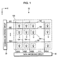
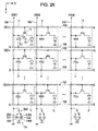
- Fig. 1 is a block diagram showing the configuration of an electro-optical device according to a first embodiment of the invention.
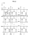
- Fig. 2 is a circuit diagram showing a detailed electrical configuration of each unit circuit.
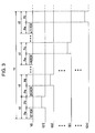
- Fig. 3 is a diagram showing the operation for driving the electro-optical device.
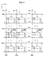
- Fig. 4 is a diagram showing the operation in a write period.
- Fig. 5 is a circuit diagram showing the configuration of an electro-optical device according to a second embodiment of the invention.
- Fig. 6 is a circuit diagram showing the configuration of an electro-optical device according to a third embodiment of the invention.
- Fig. 7 is a circuit diagram showing the configuration of an electro-optical device according to a fourth embodiment of the invention.
- Fig. 8 is a diagram showing the operation timing of the electro-optical device according to the fourth embodiment.
- Fig. 9 is a circuit diagram showing the configuration of a comparative example.
- Fig. 10 is a circuit diagram showing the configuration of an electro-optical device according to a fifth embodiment of the invention.
- Fig. 11 is a plan view of a unit circuit of an electro-optical device according to the first embodiment in a step of a manufacturing process.
- Fig. 12 is a plan view of the unit circuit of the electro-optical device according to the first embodiment in a step of the manufacturing process.
- Fig. 13 is a plan view of the unit circuit of the electro-optical device according to the first embodiment in a step of the manufacturing process.
- Fig. 14 is a plan view of the unit circuit of the electro-optical device according to the first embodiment in a step of the manufacturing process.
- Fig. 15 is a cross-section view taken along line XV - XV shown in Figs. 11 to 14 .
- Fig. 16 is a plan view of a unit circuit of an electro-optical device according to the first embodiment in a step of a manufacturing process.
- Fig. 17 is a plan view of the unit circuit of the electro-optical device according to the first embodiment in a step of the manufacturing process.
- Fig. 18 is a plan view of the unit circuit of the electro-optical device according to the first embodiment in a step of the manufacturing process.
- Fig. 19 is a plan view of the unit circuit of the electro-optical device according to the first embodiment in a step of the manufacturing process.
- Fig. 20 is a cross section view taken along line XX - XX shown in Figs. 16 to 19 .
- Fig. 21 is a plan view of a unit circuit of an electro-optical device according to the second embodiment in a step of a manufacturing process.
- Fig. 22 is a plan view of the unit circuit of the electro-optical device according to the second embodiment in a step of the manufacturing process.
- Fig. 23 is a plan view of the unit circuit of the electro-optical device according to the second embodiment in a step of the manufacturing process.
- Fig. 24 is a plan view of the unit circuit of the electro-optical device according to the second embodiment in a step of the manufacturing process.
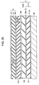
- Fig. 25 is a cross-section view taken along line XXV - XXV shown in Figs. 21 to 24 .
- Fig. 26 is a circuit diagram showing the configuration of an electro-optical device according to modified example 2 of the invention.
- Fig. 27 is a circuit diagram showing the configuration of an electro-optical device according to modified example 6 of the invention.
- Fig. 28 is a perspective view showing a detailed form of an electronic apparatus according to an embodiment of the invention.
- Fig. 29 is a perspective view showing a detailed form of an electronic apparatus according to an embodiment of the invention.
- Fig. 30 is a perspective view showing a detailed form of an electronic apparatus according to an embodiment of the invention.
- Fig. 31 is a circuit diagram showing the configuration of a general unit circuit.
- Fig. 1 is a block diagram showing the configuration of an electro-optical device 10 according to a first embodiment of the invention.
- the electro-optical device 10 is a device that is employed in various electronic apparatuses as means for displaying an image.
- the electro-optical device has a pixel array unit 100 in which a plurality of unit circuits U are arranged in a planar shape, a scanning line driving circuit 20, and a data line driving circuit 30.
- the scanning line driving circuit 20 and the data line driving circuit 30 are shown as separate circuits, however, a part or the whole of the circuits may be configured as a single circuit.
- m scanning lines 102 that extend in the direction X and n data lines 104 that extend in the direction Y perpendicular to the direction X are disposed (here, m and n are natural numbers).
- Each unit circuit U is disposed in a position corresponding to an intersection of the scanning line 102 and the data line 104. Accordingly, the unit circuits U are arranged in the shape of a matrix of vertical m rows and horizontal n columns.
- the scanning line driving circuit 20 shown in Fig. 1 is a circuit for selecting the plurality of unit circuits U in units of rows.
- the scanning line driving circuit 20 generates scanning signals G[1] to G[m] that sequentially are in an active state and outputs the scanning signals to the m scanning lines 102.
- Transition to the active state of the scanning signal G[i] supplied to the scanning line 102 of the i-th row means selection of n unit circuits U belonging to the i-th row.
- the data line driving circuit 30 shown in Fig. 1 generates data electric potentials VD[1] to VD[n] corresponding to gray scale data of the n unit circuits U of one row corresponding to the scanning line 102 selected by the scanning line driving circuit 20 and outputs the data electric potentials to the data lines 104.
- the data electric potential VD output to the j-th (where j is an integer satisfying the condition of "1 ⁇ j ⁇ n") data line 104 is denoted by VD[j].
- Fig. 2 is a circuit diagram showing a detailed electrical configuration of each unit circuit U.
- each unit circuit U has an electro-optical element 12, a capacitor element C, and a transistor Tr.
- An electro-optical element 12 is an OLED element formed by interposing a light emitting layer formed of an organic EL material between an anode and a cathode.
- the electro-optical element 12 is disposed between the transistor Tr and a constant electric potential line (ground line) to which a constant electric potential is supplied.
- the anode is disposed in each unit circuit U and is a separate electrode that is controlled for each unit circuit U.
- the cathode is configured as a common electrode that is common to the unit circuits U.
- the cathode is connected to the constant electric potential line to which a constant electric potential is supplied.
- the capacitor element C shown in Fig. 2 is a unit for maintaining the data electric potential VD[j] supplied from the data line 104. As shown in Fig. 2 , the capacitor element C has a first electrode E1 connected to a capacitor line 106 and a second electrode E2 connected to the data line 104. The capacitor line 106 to which a constant electric potential is supplied is commonly connected to the unit circuits U.
- the ground electric potential may be configured that a negative electric potential is supplied to the constant electric potential line, the data electric potential VD[N], which represent the highest luminance, of the data electric potentials VD[j] is the constant electric potential, and the data electric potential VD[1], which represents the lowest luminance, of the data electric potentials VD[j] is a negative electric potential.
- the ground electric potential may be positioned between the data electric potential VD[N] and the data electric potential VD[1]. In such a case, the amplitude of the data electric potential VD[j] with respect to the ground electric potential can decrease, and accordingly, low power consumption can be achieved.
- the N-channel-type transistor Tr shown in Fig. 2 is a switching element that is in a conductive state at a time when the scanning line 102 is selected, so that the second electrode E2 of the capacitor element C and the electro-optical element 12 are in a conductive state.
- the source of the transistor Tr is connected to the anode of the electro-optical element 12, and the drain of the transistor is connected to the data line 104 and the second electrode E2 of the capacitor element C.
- the gate of the transistor Tr is connected to the scanning line 102.
- the scanning signal G[i] transits to an active state
- the transistor Tr is in the ON state, and thereby the second electrode E2 and the electro-optical element 12 are in a conductive state.
- the transistor Tr is in the OFF state, and accordingly, the second electrode E2 and the electro-optical element 12 are in a non-conductive state.
- each unit period 1T of one vertical scanning period 1V has a write period Pw that is a time period from a start time point of the unit period 1T to a time point when a predetermined time period elapses and a drive period Pd that is a time period after the write period Pw.
- the drive period Pd is set as a time period from an end time point of the write period Pw to an end time point of the unit period 1T.
- the scanning line driving circuit 20 shown in Fig. 1 sequentially selects one scanning line 102 at a time for each drive period Pd within one unit period 1T. For example, in the i-th unit period 1T within one vertical scanning period 1V, the scanning signal G[i] is set to have the active level, and accordingly, the scanning line 102 of the i-th row is selected.
- the data line driving circuit 30 shown in Fig. 1 outputs a data electric potential VD corresponding to the gray scale data of the electro-optical element 12 of each unit circuit U corresponding to the scanning line 102 that is selected by the scanning line driving circuit 20 in the drive period Pd within each unit period 1T to each data line 104 for the write period Pw within the each unit period 1T.
- data electric potentials VD[1] to VD[n] corresponding to gray scale data of n unit circuits U of the i-th row are output to the data lines 104.
- the operation for driving the electro-optical element 12 will be described separately for the write period Pw and the drive period Pd with the unit circuits U of the i-th row focused.
- electric charges corresponding to the data electric potentials VD that are in correspondence with the gray scale data of the unit circuits U of the i-th row are charged (accumulated) in the capacitor elements C of the unit circuits U.
- electric charges corresponding to the data electric potential VD[j] that is in correspondence with the gray scale data of the j-th unit circuit U of the i-th row are charged in m capacitor elements C connected to the j-th data line 104 in a parallel manner.
- the electro-optical element 12 disposed in the j-th unit circuit U of the i-th row electric charges that are charged in the write period Pw are simultaneously supplied from m capacitor elements C connected to the j-th data line 104. Accordingly, the electro-optical elements 12 of the unit circuits U of the i-th row emit light at gray scale levels corresponding to the data electric potentials VD.
- Fig. 5 is a circuit diagram showing the configuration of an electro-optical device 10 according to a second embodiment of the invention.
- the constant electric potential line additionally serves as the capacitor line 106, which is different from the configuration of the first embodiment. Described in more details, as shown in Fig. 5 , to the constant electric potential line 108 that is commonly connected to the unit circuits U, the cathodes of the electro-optical elements 12 of the unit circuits U are commonly connected, and the first electrodes E1 of the capacitor elements C of the unit circuits U are commonly connected the constant electric potential line.
- the capacitor line 106 is not needed in addition to the constant electric potential line 108. Therefore, the configuration of the electro-optical device 10 can be simplified.
- Fig. 6 is a circuit diagram showing the configuration of an electro-optical device 10 according to a third embodiment of the invention.
- an auxiliary capacitor element Cs having one electrode connected to the data line 104 is disposed, which is different from the configuration of each of the above-described embodiments.
- Other configurations are the same as those of the above-described embodiments, and thus, descriptions of duplicate parts thereof are omitted here.
- one electrode E3 of the auxiliary capacitor element Cs is connected to the data line 104, and the other electrode E4 thereof is connected to the electric potential line to which a constant electric potential is supplied.
- the auxiliary capacitor element Cs is also charged.
- electric charges transferred from the auxiliary capacitor element Cs are supplied to the unit circuit U corresponding to the auxiliary capacitor element Cs.
- the electric potential line for example, may be the capacitor line 106 shown in Fig. 2 or the constant electric potential line 108 shown in Fig. 5 .
- the lacking amount can be supplemented by using the capacitance of the auxiliary capacitor element Cs connected to the data line 104.
- Fig. 7 is a circuit diagram showing the configuration of an electro-optical device 10 according to a fourth embodiment of the invention.
- each data line 104 is connected to m unit circuits U and is configured by a first part Z1 having a same length for each data line 104 and a second part Z2 connected to the data line driving circuit 30.
- the data line driving circuit 30 is disposed in the center of the pixel array unit 100 in direction X, and each data line 104 is bent so as to be connected to the data line driving circuit 30.
- the range of the pixel array unit 100 in which the data lines 104 are distributed in direction X is broader than the range in which the output terminals of the data lines 104 are distributed in the data line driving circuit 30, and accordingly, lengths of the data lines 104 are different from one another.
- the first parts Z1 of the data lines 104 have a same length, and thus, the lengths of the second parts Z2 of the data lines 104 are different from one another.
- a switch Sw that is used for switching the first and second parts between a conductive state and a non-conductive state is disposed.
- the switches Sw are controlled to be in the ON state or the OFF state all together by a control circuit not shown in the figure.
- the other configurations are the same as those of each of the above-described embodiments.
- the switch Sw is in the ON state for each write period Pw of one unit period 1T and is in the OFF state for each drive period Pd of the unit period 1T. Described in more details, in the write period Pw, the switches Sw are in the ON state all together, and the data lines 104 and the data line driving circuit 30 are in the conductive state. Accordingly, electric charges corresponding to the data electric potentials VD output from the data line driving circuit 30 are supplied to the data lines 104. On the other hand, in the drive period Pd, the switches Sw are in the OFF state all together, and the data lines 104 and the data line driving circuit 30 are in the non-conductive state. Accordingly, supply of the electric charges corresponding to the data electric potentials VD to the data lines 104 from the data line driving circuit 30 is stopped.
- Fig. 9 is a circuit diagram showing the configuration (hereinafter, referred to as a comparative example) in which the switch Sw is not disposed in each data line 104 and the first part Z1 and the second part Z2 are connected continuously.
- a comparative example parasitic capacitance not shown in the figure is included.
- the lengths of the second parts Z2 of the data lines 104 are different from one another.
- values of the parasitic capacitance of the data lines 104 are unbalanced. Accordingly, there is a problem that the amounts of light emission of the electro-optical elements 12 disperse for the data lines 104.
- the second parts Z2 having different lengths for the data lines 104 are separated from the data lines 104 in the drive period Pd.
- the lengths of the first parts Z1 of the data lines 104 are the same.
- the electric charges supplied to the electro-optical elements 12 of the unit circuits U of the row are uniform.
- Fig. 10 is a circuit diagram showing the configuration of an electro-optical device 10 according to a fifth embodiment of the invention.
- the capacitor element C is not disposed in each unit circuit U, which is different from the above-described embodiments.
- each unit circuit U has an electro-optical element 12 and a transistor Tr.
- the transistor Tr is disposed between a data line 104 and the electro-optical element 12 and is a unit that is in a conductive state at a time when a scanning line 102 is selected for making the data line and the electro-optical element to be in a conductive state.
- each of n data lines has a first part Z1 to which m unit circuits U are connected, a second part Z2 that is connected to a data line driving circuit 30, and a switch Sw that is interposed between the first part Z1 and the second part Z2.
- Each switch Sw is in a conductive state for each write period Pw so as to make the first part Z1 and the second part Z2 to be in a conductive state.
- each switch Sw is in a non-conductive state for each drive period Pd so as to make the first part Z1 and the second part Z2 to be in a non-conductive state.
- the switches Sw as in the fourth embodiment, are controlled to be in the ON state or the OFF state all together by a control circuit not shown in the figure.
- the operation of the electro-optical device 10 according to this embodiment is the same as that according to the fourth embodiment.
- the switches Sw are in the ON state all together. Accordingly, the data lines 104 and the data line driving circuit 30 are in the conductive state, and thereby data electric potentials VD[1] to VD[n] output from the data line driving circuit 30 are supplied to the data lines 104.
- the data electric potentials VD[1] to VD[n] corresponding to each gray scale data of the n unit circuits U that are selected in the drive period Pd of the i-th unit period 1T are supplied to the data lines 104. Accordingly, electric charges corresponding to the data electric potentials VD[1] to VD[n] are charged in capacitance (parasitic capacitance) that is accompanied in each data line 104.
- the length of the first part Z1 of each data line 104 is sufficiently larger than that of the second part Z2, and thus the value of parasitic capacitance generated between the first part Z1 and other elements (the scanning lien 102, the power supply line, and neighbor data lines 104, and the like) is sufficiently larger that generated between the second part Z2 and other elements. Accordingly, in the write period Pw of each unit period 1T, most of the electric charges according to the data electric potentials VD[1] to VD[n] output from the data line driving circuit 30 are charged in the capacitance accompanied in the first part Z1 of the data lines 104.
- the switches Sw are in the OFF state all together. Accordingly, the first part Z1 of each data line 104 is electrically separated from the data line driving circuit 30, and supply of the data electric potentials VD[1] to VD[n] from the data line driving circuit 30 to the data lines 104 is stopped.
- one scanning line 102 is selected by the scanning line driving circuit 20. To the electro-optical elements 12 of the unit circuits U corresponding to the selected scanning line 102, the electric charges charged in the write period Pw are supplied from the capacitance accompanied by the first parts Z1 of the data lines 104 corresponding to the unit circuits U.
- the electric charges charged in the capacitance accompanied in one data line 104 can be used for light emission of one electro-optical element 12. Accordingly, differently from the above-described embodiments, the capacitor element is not needed to be disposed in each unit circuit U. As a result, according to this embodiment, there is an advantage that high precision can be achieved, compared to a case where the configuration in which the capacitor element is disposed in each unit circuit U is used.
- the lengths of the first parts Z1 of the data lines 104 may be configured to be the same.
- the values of capacitance accompanied by the first parts Z1 of the data lines 104 can be uniform, and electric charges supplied to the electro-optical elements 12 of the unit circuits U of a row are uniform in a case where gray scale data of the unit circuits U of the row selected in the drive period Pd is the same.
- Figs. 11 to 14 are plan views showing appearances of each step in which the unit circuit U of the electro-optical device 10 according to the first embodiment is formed.
- Figs. 11 to 14 six unit circuits U in each stage are arranged in the direction X and the direction Y.
- Fig. 15 is a cross-section view taken along line XV - XV shown in Figs. 11 to 14 .
- Figs. 11 to 14 are plan views, for easy understanding of each element, to each element common to that shown in Fig. 15 , a same hatching pattern as that shown in Fig. 15 is appropriately used.
- a semiconductor layer 41 formed of a semiconductor material such as silicon is formed on the face of a substrate 40.
- the semiconductor layer 41 has a first part 41a and a second part 41b that extend in direction Y and a connection part 41c that extends in direction X and connects the first and second parts.
- the first part 41a serves as a drain region and also serves as a second electrode E2 of a capacitor element C of each unit circuit U.
- the second part 41b serves as a source region.
- the connection part 41c serves as a channel region.
- the entire surface of the substrate 40 on which the semiconductor layer 41 is formed is covered with a first insulating layer Fa1.
- a gate electrode 43 (scanning line 102) of the transistor Tr and a capacitor line 106 are formed on the face of the first insulating layer Fa1.
- the gate electrode 43 and the capacitor line 106 are formed together in a same process by patterning a conductive film (for example, a thin film made of aluminum) that is continuously formed over the entire area of the first insulating layer Fa1.
- the gate electrode 43 extends in direction X and is overlapped with the connection part 41c (gate region) of the semiconductor layer 41 through the first insulating layer Fa1 (not shown in Fig. 12 ).
- the capacitor line 106 serves as the first electrode E1 of the capacitor element C of each unit circuit U. As shown in Fig. 12 , the capacitor line 106 extends in direction X and is overlapped with the first part 41a of the semiconductor layer 41 through the first insulating layer Fa1 (not shown in Fig. 12 ). As shown in Fig. 15 , the capacitor line 106 (the first electrode E1) and the first part 41a (the second electrode E2) of the semiconductor layer 41 face each other with the first insulating layer Fa1 interposed therebetween, and thereby a capacitor C1 is formed.
- forming a plurality of elements by selectively removing a common film body (regardless of a single layer or a plurality of layers) in a same process will be represented only by "forming from a same layer", hereinafter.
- Elements formed from the same layer are naturally made of a same material, and film thicknesses thereof are approximately the same with one another.
- the entire surface of the first insulating layer Fa1 on which the gate electrode 43 and the capacitor line 106 are formed is covered with a second insulating layer Fa2.
- the data line 104 is formed on the face of the second insulating layer Fa2.
- the data line 104 is formed by patterning a conductive film (for example, a thin film made of aluminum) that is continuously formed over the entire area of the second insulating layer Fa2.
- the data line 104 extends in direction Y and is overlapped with the capacitor line 106 through the second insulating layer Fa2 (not shown in Fig. 13 ).
- the data line 104 and the capacitor line 106 face each other with the second insulating layer Fa2 interposed therebetween, and thereby a capacitor C2 is formed.
- the capacitor element C of each unit circuit U is formed by the capacitor C1 formed by bringing the first part 41a (the second electrode E2) of the semiconductor layer 41 and the capacitor line 106 (the first electrode E1) to face each other with the first insulating layer Fa1 interposed therebetween and the capacitor C2 formed by bringing the capacitor line 106 and the data line 104 to face each other with the second insulating layer Fa2 interposed therebetween.
- a plurality of capacitors that are formed in the direction of lamination in each unit circuit U forms the capacitor element C, and accordingly, the capacitance value of the capacitor element C in each unit circuit U can be sufficiently acquired.
- This configuration is particularly effective for a case where high definition of pixels is performed and the area of a planar part in each unit circuit U decreases.
- the data line 104 also serves as the drain electrode of the transistor Tr in each unit circuit U. As shown in Figs. 13 and 15 , the data line 104 and the first part 41a (the drain region) of the semiconductor layer 41 are in the conductive state through a contact hole CH.
- the source electrode 45 of the transistor Tr and the data line 104 are formed in a same layer, and the source electrode and the second part 41b (the source region) of the semiconductor layer 41 are in the conductive state through a contact hole CH2.
- the entire surface of the second insulating layer Fa2 on which the data line 104 is formed is covered with a third insulating layer Fa3.
- a third insulating layer Fa3 As shown in Figs. 14 and 15 , on the face of the third insulating layer Fa3, an anode 13 of the electro-optical element 12 is formed.
- the source electrode 45 of the transistor Tr and the anode 13 are in the conductive state through a contact hole CH3.
- various light-reflective conduction materials such as metal including aluminum, silver, or the like and alloy using the above-described material as a major component are used.
- a partition wall 14 used for dividing each unit circuit U is formed on the face of the third insulating layer Fa3 on which the anode 13 is formed.
- a light emitting layer 15 of the electro-optical element 12 is formed at least in a depression that is surrounded by the inner peripheral face of the partition wall 14 and has the anode 13 as its bottom.
- the light emitting element 15 may be formed on the partition wall 14.
- various function layers a hole injecting layer, a hole transport layer, an electron injecting layer, an electron transport layer, a hole blocking layer, and an electron blocking layer used for promoting or effectively performing the light emission of the light emitting layer 15 are laminated on the light emitting layer 15 may be used.
- a cathode 16 is formed so as to cover the light emitting layer 15 and the partition wall 14 of each unit circuit U.
- the cathode 16 is formed to be continuous over the electro-optical elements 12 of the unit circuits U.
- the cathode 16 is formed of a transparent conduction material such as ITO (Indium Tin Oxide) or IZO (Indium Zinc Oxide).
- the cathode 16 may be formed to include a material having a low work function such as alloy of Mg and Ag at a thickness for which light can be transmitted.
- light that is irradiated from the light emitting layer 15 to the cathode 16 side of the electro-optical element 12 and light that is irradiated to a side opposite to the cathode 16 from the light emitting layer 15, reflected from the anode 13, and forwarded toward the cathode 16 are transmitted through the cathode 16 to be output externally (top emission).
- the electro-optical device 10 may employ a bottom-emission-type structure.
- Figs. 16 to 19 are plan views showing appearances of each step in which each unit circuit U is formed in a case where the electro-optical device 10 is configured as the bottom-emission-type.
- Fig. 20 is a cross section view taken along line XX - XX shown in Figs. 16 to 19 .
- a semiconductor layer 51 is formed of a semiconductor material such as silicon.
- the semiconductor layer 51 has a first part 51a that extends in direction Y and a second part 51b that extends in direction X.
- the first part 51a serves as a drain region of the transistor Tr and also serves as a second electrode E2 of a capacitor element C.
- the second part 51b serves as a channel region and a source region.
- the entire surface of the substrate 50 on which the semiconductor layer 51 is formed is covered with a first insulating layer Fb1.
- a gate electrode 53 (scanning line 102) of a transistor Tr and a capacitor line 106 are formed on the face of the first insulating layer Fb1.
- the gate electrode 53 and the capacitor line 106 are formed in a same layer.
- the gate electrode 53 has a first part 53a that extends in direction X and a second part 53b that extends in direction Y.
- the first part 53a serves as a scanning line 102.
- the second part 53b is overlapped with the second part 51b (channel region) of the semiconductor layer 51 through the first insulating layer Fb1 (not shown in Fig. 17 ).
- the capacitor line 106 has a first part 106a that extends in direction X and a second part 106b that extends in direction Y.
- the second part 106b of the capacitor line 106 is overlapped with the first part 51a of the semiconductor layer 51 through the first insulating layer Fb1 (not shown in Fig. 17 ).
- the second part 106b (the first electrode E1) of the capacitor line 106 and the first part 51a (the second electrode E2) of the semiconductor layer 51 face each other with the first insulating layer Fb1 interposed therebetween, and thereby a capacitor C11 is formed.
- the entire surface of the first insulating layer Fb1 in which the gate electrode 53 and the capacitor line 106 are formed is covered with a second insulating layer Fb2.
- the data line 104 is formed on the face of the second insulating layer Fb2.
- the data line 104 extends in direction Y and is overlapped with the second part 106b of the capacitor line 106 through the second insulating layer Fb2 (not shown in Fig. 18 ).
- Fig. 18 the data line 104 extends in direction Y and is overlapped with the second part 106b of the capacitor line 106 through the second insulating layer Fb2 (not shown in Fig. 18 ).
- the data line 104 and the second part 106b of the capacitor line 106 face each other with the second insulating layer Fb2 interposed therebetween, and thereby a capacitor C22 is formed.
- the capacitor element C of each unit circuit U is formed by the capacitor C11 formed by bringing the first part 51a (the first electrode E1) of the semiconductor layer 51 and the second part 106b (the second electrode E2) of the capacitor line 106 to face each other with the first insulating layer Fb1 interposed therebetween and the capacitor C22 formed by bringing the second part 106b of the capacitor line 106 and the data line 104 to face each other with the second insulating layer Fb2 interposed therebetween.
- the data line 104 and the first part 51a (the drain region) of the semiconductor layer 51 are in the conductive state through a contact hole CH.
- the source electrode 55 of the transistor Tr and the data line 104 are formed in a same layer, and the source electrode and the second part 51b (the source region) of the semiconductor layer 51 are in the conductive state through a contact hole CH2.
- the entire surface of the second insulating layer Fb2 on which the data line 104 is formed is covered with a third insulating layer Fb3.
- a third insulating layer Fb3 As shown in Figs. 19 and 20 , on the face of the third insulating layer Fb3, an anode 13 of the electro-optical element 12 is formed.
- the source electrode 55 of the transistor Tr and the anode 13 are in the conductive state through a contact hole CH3.
- the anode 13 is formed of a transparent conduction material.
- a partition wall 14 is formed on the face of the third insulating layer Fb3 on which the anode 13 is formed.
- a light emitting layer 15 of the electro-optical element 12 is formed at least in a depression that is surrounded by the inner peripheral face of the partition wall 14 and has the anode 13 as its bottom.
- a cathode 16 is formed so as to cover the light emitting layer 15 and the partition wall 14 of each unit circuit U.
- the cathode 16 is formed of a light-reflective conduction material.
- the cathode 16 may be formed to include a material having light-reflectivity such as aluminum or silver and a material having a low work function such as magnesium or calcium.
- light that is irradiated from the light emitting layer 15 to the anode 13 side of the electro-optical element 12 and light that is irradiated to the cathode 16 side from the light emitting layer 15, reflected from the cathode 16, and forwarded toward the anode 13 are output through the anode 13 (bottom emission).
- Figs. 21 to 24 are plan views showing appearances of each step in which the unit circuit U of the electro-optical device 10 according to the second embodiment is formed.
- Figs. 21 to 24 four unit circuits U in each stage are arranged in the direction X and the direction Y.
- Fig. 25 is a cross-section view taken along line XXV - XXV shown in Figs. 21 to 24 .
- Figs. 21 to 24 are plan views, for easy understanding of each element, to each element common to that shown in Fig. 25 , a same hatching pattern as that shown in Fig. 25 is appropriately used.
- semiconductor layers 61 and 71 formed of a semiconductor material such as silicon is formed on the face of a substrate 60.
- a semiconductor layer 61 extends in direction X and serves as a channel region of the transistor Tr.
- the semiconductor layer 71 serves as a first electrode E1 of the capacitor element C.
- the entire surface of the substrate 60 on which the semiconductor layer 61 and the semiconductor layer 71 are formed is covered with a first insulating layer Fc1.
- a gate electrode 63 (the scanning line 102) of the transistor Tr and a wiring 80 formed of a conductive material are formed on the face of the first insulating layer Fc1.
- the gate electrode 63 and the wiring 80 are formed in a same layer.
- the gate electrode 63 has a first part 63a that extends in direction X and a second part 63b that extends in direction Y.
- the first part 63a of the gate electrode 63 serves as the scanning line 102.
- the second part 63b of the gate electrode 63 is overlapped with the semiconductor layer 61 (the channel region) through the first insulating layer Fc1 (not shown in Fig. 22 ).
- the wiring 80 has a first part 80a having a rectangular shape and second parts 80b that extend from the edges of the first part 80a to the positive and negative sides of direction Y.
- the first part 80a of the wiring 80 also serves as a second electrode E2 of the capacitor element C.
- the first part 80a of the wiring 80 is overlapped with the semiconductor layer 71 (the first electrode E1).
- the semiconductor layer 71 (the first electrode E1) and the first part 80a (the second electrode E2) of the wiring 80 face each other with the first insulating layer Fc1 interposed therebetween, and thereby a capacitor C111 is formed.
- the entire surface of the first insulating layer Fc1 in which the gate electrode 63 and the wiring 80 are formed is covered with a second insulating layer Fc2.
- the drain electrode 65, the source electrode 67, and the constant electric potential line 108 are formed on the face of the second insulating layer Fc2.
- the drain electrode 65, the source electrode 67, and the constant electric potential line 108 are formed in a same layer.
- the drain electrode 65 has a first part 65a that extends in direction Y and a second part 65b that extends in direction X. As shown in Fig. 23 , the first part 65a of the drain electrode 65 and the second part 80b of the wiring 80 are connected together (conductive to each other) through a contact hole CH so as to form the data line 104. In addition, as shown in Fig. 23 , the second part 65b of the drain electrode 65 and the semiconductor layer 61 (the drain region) are in the conductive state through a contact hole CH2.
- the source electrode 67 extends in direction X so as to be in the conductive state with the semiconductor layer 61 (the source region) through a contact hole CH3.
- the constant electric potential line 108 that is formed of metal having low resistance extends in direction X so as to be overlapped with the first part 80a of the wiring 80.
- the constant electric potential line 108 and the first part 80a of the wiring 80 face each other with the second insulating layer Fc2 interposed therebetween, and thereby a capacitor C222 is formed.
- the capacitor element C of each unit circuit U is formed by the capacitor C111 formed by bringing the semiconductor layer 71 (the first electrode E1) of the semiconductor layer 71 and the first part 80a (the second electrode E2) of the wiring 80 to face each other with the first insulating layer Fc1 interposed therebetween and the capacitor C222 formed by bringing the constant electric potential line 108 and the first part 80a of the wiring 80 to face each other with the second insulating layer Fc2 interposed therebetween.
- the constant electric potential line 108 is connected to the semiconductor layer 71 (the first electrode E1) through a contact hole CH4.
- the entire surface of the second insulating layer Fc2 on which the drain electrode 65, the source electrode 67, and the constant electric potential line 108 are formed is covered with a third insulating layer Fc3.
- the anode 13 of the electro-optical element 12 and an intermediate conductive layer 90 are formed on the face of the third insulating layer Fc3.
- the anode 13 and the intermediate conductive layer 90 are formed in a same layer.
- the source electrode 67 of the transistor Tr and the anode 13 are in the conductive state through a contact hole CH5.
- the anode 13 is formed of a light-reflective conduction material.
- the constant electric potential line 108 and the intermediate conductive layer 90 are in the conductive state through a contact hole CH6.
- a partition wall 14 is formed on the face of the third insulating layer Fc3 on which the anode 13 and the intermediate conductive layer 90 are formed.
- a light emitting layer 15 of the electro-optical element 12 is formed in the shape of a depression that is surrounded by the inner peripheral face of the partition wall 14 and has the anode 13 as its bottom.
- the cathode 16 is formed so as to cover the anode 13 (not shown in Fig. 25 ), the partition wall 14, and the intermediate conductive layer 90 of each unit circuit U.
- the cathode 16 is formed to be continuous over the electro-optical elements 12 of the unit circuits U.
- the cathode 16 is in a conductive state with the intermediate conductive layer 90 through a contact hole CH7.
- the constant electric potential line 108 not only serves as one electrode of the capacitor element C but also serves as an auxiliary electrode used for decreasing the resistance of the cathode 16.
- the cathode 16 is formed of a transparent conduction material such as ITO (Indium Tin Oxide) or IZO (Indium Zinc Oxide).
- ITO Indium Tin Oxide
- IZO Indium Zinc Oxide
- light that is irradiated from the light emitting layer 15 to the cathode 16 side of the electro-optical element 12 and light that is irradiated to a side opposite to the cathode 16 from the light emitting layer 15, reflected from the anode 13, and forwarded toward the cathode 16 are transmitted through the cathode 16 to be output externally (top emission).
- the invention is not limited thereto, and a bottom-emission-type structure may be employed.
- the cathode 16 is formed of a high-resistance material such as ITO.
- the resistance of the cathode 16 can decrease by making the constant electric potential line 108 formed of a metal material having resistance lower than that of the cathode 16 and the cathode 16 to be in the contact state through contact holes CH6 and CH7. Accordingly, a voltage drop in the cathode 16 is suppressed.
- the static electric potential line 108 not only serves as the capacitor line 106 but also serves as an auxiliary wiring.
- the invention is not limited thereto, and, for example, a configuration in which the write period Pw starts after a predetermined time elapses from the start time point of the unit period 1T may be used.
- a case where the end time point of the write period Pw of each unit time 1T and the start time point of the drive time Pd are the same is exemplified.
- the invention is not limited thereto, and, for example, a configuration in which the drive time Pd starts before the write time Pw ends may be used.
- auxiliary capacitor element Cs having one electrode connected to the data line 104 is disposed in addition to the capacitor element C of each unit circuit U.
- auxiliary capacitor element Cs includes a plurality of capacitor elements having different capacitance values and a switching element that makes one capacitor element among the plurality of capacitor elements and the data line 104 in the conductive state is disposed between one electrode of each of the plurality of capacitor elements and the data line 104 may be used.
- Fig. 26 is a circuit diagram showing the configuration of an electro-optical device 10 according to modified example 2.
- the auxiliary capacitor element Cs is configured by a first capacitor element Cs1 and a second capacitor element Cs2 having different capacitance values (for example, the capacitance of Cs1 > the capacitance of Cs2).
- a switch Sw2 that makes one capacitor element between the first capacitor element Cs1 and the second capacitor element Cs2 and the data line 104 is disposed.
- the other electrode E40 of the first capacitance Cs1 and the other electrode E400 of the second capacitor element Cs2 are connected commonly to a constant power supply line to which a constant electric potential is supplied.
- the constant electric potential line for example, may be the capacitor line 106 shown in Fig. 2 or the constant electric potential line 108 shown in Fig. 5 .
- the switch Sw2 is controlled by a control circuit not shown in the figure.
- the write period Pw of each unit period 1T one between the first capacitor element Cs1 and the second capacitor element Cs2 is selected by the switch Sw2 to be conductive to the data line 104, and the selected capacitor element is charged.
- the drive period Pd of each unit period 1T electric charges from the capacitor element is supplied to a corresponding unit circuit U.
- an emission time of the electro-optical element 12 can be controlled. Accordingly, the amount of light emission of the electro-optical element 12 can be controlled at a plurality of levels.
- the auxiliary capacitor element Cs is configured by the first capacitor element Cs1 and the second capacitor element Cs2 in the configuration shown in Fig. 26 .
- the invention is not limited thereto, and the auxiliary capacitor element Cs is needed to include a plurality of capacitor elements having different capacitance values.
- the auxiliary capacitor element Cs may be configured by three capacitor elements having three different capacitance values. As the number of the capacitor elements having different capacitance values increases, there is an advantage that the capacitance value can be more delicately controlled.
- the transistor Tr of each unit circuit U is the N-channel type transistor.
- the invention is not limited thereto, and the transistor may be configured by a P-channel type transistor.
- the transistor Tr is configured as a switching element to be conductive at a time when the scanning line 102 is selected for making the second electrode E2 of the capacitor element C and the electro-optical element 12 to be in the conductive state.
- the switch Sw used for switching between conduction and non-conduction of the first and second parts is disposed between the first part Z1 and the second part Z2.
- the switch Sw may be configured by a thin film transistor, an N-channel type transistor, or a P-channel type transistor.
- an OLED has been described.
- an organic light emitting diode or an LED Light Emitting Diode
- an element of any type may be used as the electro-optical element as long as the element emits light at a light-emission luminance level corresponding to an electrical energy level.
- a configuration in which electric charges corresponding to the data electric potential VD are charged in the capacitance (parasitic capacitance) accompanied in the data line 104 has been exemplified.
- a configuration in which a capacitor element Cx used for charging electric charges in correspondence with the data electric potential VD is disposed in each data line 104 (the first part Z1) may be used. Even in such a case, as in the fifth embodiment, the capacitor element is not needed to be disposed in each unit circuit U. Accordingly, there is an advantage that high definition can be achieved.
- the number of the capacitor elements Cx disposed in each data line 104 may be one, or two or more.
- the position of the capacitor element Cx disposed in each data line 104 can be arbitrarily set.
- Fig. 28 is a perspective view showing the configuration of a mobile personal computer that uses the electro-optical device 10 according to any one of the above-described embodiments as a display unit.
- the personal computer 2000 includes a light emitting unit 10 as the display unit and a main body 2010. In the main body 2010, a power switch 2001 and a keyboard 2002 are disposed. Since the electro-optical device 10 uses the OLED element as the electro-optical element 12, a screen that has a wide viewing angle and can be easily viewed can be displayed.
- Fig. 29 shows the configuration of a cellular phone to which the electro-optical device 10 according to an embodiment of the invention is used.
- the cellular phone 3000 includes a plurality of operation buttons 3001, a scroll button 3002 and an electro-optical device 10 as a display unit. By operating the scroll button 3002, a screen displayed in the electro-optical device 10 is scrolled.
- Fig. 30 shows the configuration of a personal digital assistant (PDA) to which the electro-optical device 10 according to an embodiment of the invention is used.
- the personal digital assistant 4000 includes a plurality of operation buttons 4001, a power switch 4002, and the electro-optical device 10 as a display unit. By operating the power switch 4002, various types of information such as an address book or a schedule planner are displayed in the electro-optical device 10.
- an electro-optical device in addition to the electronic apparatuses shown in Figs. 28 to 30 , there are a digital camera, a television set, a video camera, a car navigation system, a pager, an electronic organizer, an electronic paper sheet, a calculator, a word processor, a workstation, a video phone, a POS terminal, a printer, a scanner, a copier, a video player, an apparatus having a touch panel, and the like.
- the use of the electro-optical device according to an embodiment of the invention is not limited to display of an image.
- an image forming device such as an optical write-type printer or an electronic copier
- a write head that exposes a photosensitive body in accordance with an image to be formed in a writing material such as a paper sheet
- the electro-optical device according to an embodiment of the invention can be also used for the write head of such type.
- An electronic circuit described in the embodiments of the invention includes a circuit that becomes a unit for exposure in an image forming device, in addition to a pixel circuit constituting pixels of the display device as in the above-described embodiments.
Landscapes
- Engineering & Computer Science (AREA)
- Physics & Mathematics (AREA)
- Computer Hardware Design (AREA)
- General Physics & Mathematics (AREA)
- Theoretical Computer Science (AREA)
- Geometry (AREA)
- Microelectronics & Electronic Packaging (AREA)
- Control Of Indicators Other Than Cathode Ray Tubes (AREA)
- Control Of El Displays (AREA)
- Electroluminescent Light Sources (AREA)
Applications Claiming Priority (2)
| Application Number | Priority Date | Filing Date | Title |
|---|---|---|---|
| JP2008026580 | 2008-02-06 | ||
| JP2008236499A JP5359141B2 (ja) | 2008-02-06 | 2008-09-16 | 電気光学装置、その駆動方法、電子機器 |
Publications (2)
| Publication Number | Publication Date |
|---|---|
| EP2088577A2 true EP2088577A2 (fr) | 2009-08-12 |
| EP2088577A3 EP2088577A3 (fr) | 2011-03-16 |
Family
ID=40668381
Family Applications (1)
| Application Number | Title | Priority Date | Filing Date |
|---|---|---|---|
| EP09001504A Withdrawn EP2088577A3 (fr) | 2008-02-06 | 2009-02-04 | Dispositif électro-optique, procédé de commande de celui-ci, et appareil électronique |
Country Status (4)
| Country | Link |
|---|---|
| US (1) | US8610644B2 (fr) |
| EP (1) | EP2088577A3 (fr) |
| JP (1) | JP5359141B2 (fr) |
| KR (1) | KR20090086150A (fr) |
Cited By (2)
| Publication number | Priority date | Publication date | Assignee | Title |
|---|---|---|---|---|
| WO2012155560A1 (fr) * | 2011-07-07 | 2012-11-22 | 中兴通讯股份有限公司 | Procédé et système de commande d'affichage |
| EP2562743A1 (fr) * | 2011-08-23 | 2013-02-27 | Sony Corporation | Dispositif d`affichage et appareil électronique |
Families Citing this family (9)
| Publication number | Priority date | Publication date | Assignee | Title |
|---|---|---|---|---|
| JP5439913B2 (ja) | 2009-04-01 | 2014-03-12 | セイコーエプソン株式会社 | 電気光学装置及びその駆動方法、並びに電子機器 |
| JP5439912B2 (ja) * | 2009-04-01 | 2014-03-12 | セイコーエプソン株式会社 | 電気光学装置及びその駆動方法並びに電子機器 |
| JP2010249978A (ja) * | 2009-04-14 | 2010-11-04 | Seiko Epson Corp | 電気光学装置及びその駆動方法並びに電子機器 |
| JP2010250210A (ja) | 2009-04-20 | 2010-11-04 | Seiko Epson Corp | 電気光学装置及びその駆動方法、並びに電子機器 |
| JP5879944B2 (ja) | 2011-11-16 | 2016-03-08 | セイコーエプソン株式会社 | 電気光学装置、および電子機器 |
| JP5821685B2 (ja) * | 2012-02-22 | 2015-11-24 | セイコーエプソン株式会社 | 電気光学装置および電子機器 |
| JP2020027270A (ja) * | 2018-08-13 | 2020-02-20 | セイコーエプソン株式会社 | 電気光学装置および電子機器 |
| CN110767106B (zh) | 2018-09-30 | 2020-09-08 | 云谷(固安)科技有限公司 | 显示面板、显示屏及显示终端 |
| WO2023149105A1 (fr) * | 2022-02-04 | 2023-08-10 | 株式会社ジャパンディスプレイ | Dispositif d'affichage |
Citations (3)
| Publication number | Priority date | Publication date | Assignee | Title |
|---|---|---|---|---|
| US5714968A (en) * | 1994-08-09 | 1998-02-03 | Nec Corporation | Current-dependent light-emitting element drive circuit for use in active matrix display device |
| JP2000122608A (ja) | 1998-10-13 | 2000-04-28 | Seiko Epson Corp | 表示装置及び電子機器 |
| US20060267885A1 (en) * | 2005-05-12 | 2006-11-30 | Won-Kyu Kwak | Organic light emitting display |
Family Cites Families (27)
| Publication number | Priority date | Publication date | Assignee | Title |
|---|---|---|---|---|
| GB2081018B (en) | 1980-07-31 | 1985-06-26 | Suwa Seikosha Kk | Active matrix assembly for display device |
| JP2689917B2 (ja) * | 1994-08-10 | 1997-12-10 | 日本電気株式会社 | アクティブマトリクス型電流制御型発光素子の駆動回路 |
| JP3471928B2 (ja) | 1994-10-07 | 2003-12-02 | 株式会社半導体エネルギー研究所 | アクティブマトリクス表示装置の駆動方法 |
| JPH08329992A (ja) * | 1995-05-29 | 1996-12-13 | Saitama Nippon Denki Kk | 電池パックと充電器 |
| JP2000242234A (ja) * | 1999-02-19 | 2000-09-08 | Toshiba Corp | 平面表示装置 |
| JP4406951B2 (ja) * | 1999-03-25 | 2010-02-03 | Tdk株式会社 | 薄膜発光素子の駆動方法および駆動回路 |
| JP3757797B2 (ja) * | 2001-01-09 | 2006-03-22 | 株式会社日立製作所 | 有機ledディスプレイおよびその駆動方法 |
| JP2003066871A (ja) * | 2001-08-28 | 2003-03-05 | Sony Corp | 有機el表示装置及びその製造方法 |
| JP3819760B2 (ja) * | 2001-11-08 | 2006-09-13 | 株式会社日立製作所 | 画像表示装置 |
| TWI284876B (en) * | 2002-08-19 | 2007-08-01 | Toppoly Optoelectronics Corp | Device and method for driving liquid crystal display |
| JP2004145300A (ja) * | 2002-10-03 | 2004-05-20 | Seiko Epson Corp | 電子回路、電子回路の駆動方法、電子装置、電気光学装置、電気光学装置の駆動方法及び電子機器 |
| US6911964B2 (en) * | 2002-11-07 | 2005-06-28 | Duke University | Frame buffer pixel circuit for liquid crystal display |
| JP3687648B2 (ja) | 2002-12-05 | 2005-08-24 | セイコーエプソン株式会社 | 電源供給方法及び電源回路 |
| JP4604455B2 (ja) * | 2003-04-08 | 2011-01-05 | セイコーエプソン株式会社 | 電気光学装置、電気光学装置の駆動方法及び電子機器 |
| US7408577B2 (en) * | 2003-04-09 | 2008-08-05 | Micron Technology, Inc. | Biasing scheme for large format CMOS active pixel sensors |
| JP4784050B2 (ja) * | 2004-06-18 | 2011-09-28 | セイコーエプソン株式会社 | 電子回路、その制御方法、電気光学装置および電子機器 |
| KR100649246B1 (ko) * | 2004-06-30 | 2006-11-24 | 삼성에스디아이 주식회사 | 역다중화 장치와, 이를 이용한 표시 장치 및 그 표시 패널 |
| KR100662978B1 (ko) * | 2004-08-25 | 2006-12-28 | 삼성에스디아이 주식회사 | 발광 표시장치와 그의 구동방법 |
| JP4752315B2 (ja) * | 2005-04-19 | 2011-08-17 | セイコーエプソン株式会社 | 電子回路、その駆動方法、電気光学装置および電子機器 |
| JP2007041229A (ja) * | 2005-08-02 | 2007-02-15 | Toshiba Matsushita Display Technology Co Ltd | アクティブマトリクス型液晶表示装置 |
| KR101322195B1 (ko) * | 2005-09-15 | 2013-11-04 | 가부시키가이샤 한도오따이 에네루기 켄큐쇼 | 표시 장치 및 이의 구동 방법 |
| US7616179B2 (en) * | 2006-03-31 | 2009-11-10 | Canon Kabushiki Kaisha | Organic EL display apparatus and driving method therefor |
| JP5275551B2 (ja) * | 2006-06-02 | 2013-08-28 | 富士フイルム株式会社 | 電流制御型駆動回路および表示装置 |
| JP4203773B2 (ja) * | 2006-08-01 | 2009-01-07 | ソニー株式会社 | 表示装置 |
| KR100739335B1 (ko) * | 2006-08-08 | 2007-07-12 | 삼성에스디아이 주식회사 | 화소 및 이를 이용한 유기전계발광 표시장치 |
| TWI358008B (en) * | 2006-12-12 | 2012-02-11 | Ind Tech Res Inst | Pixel structure of display device and method for d |
| EP2613305B1 (fr) * | 2008-10-07 | 2017-02-22 | Joled Inc. | Dispositif afficheur d'image, et procédé de commande correspondant |
-
2008
- 2008-09-16 JP JP2008236499A patent/JP5359141B2/ja active Active
-
2009
- 2009-01-07 KR KR1020090001006A patent/KR20090086150A/ko not_active Withdrawn
- 2009-02-04 EP EP09001504A patent/EP2088577A3/fr not_active Withdrawn
- 2009-02-04 US US12/365,358 patent/US8610644B2/en active Active
Patent Citations (3)
| Publication number | Priority date | Publication date | Assignee | Title |
|---|---|---|---|---|
| US5714968A (en) * | 1994-08-09 | 1998-02-03 | Nec Corporation | Current-dependent light-emitting element drive circuit for use in active matrix display device |
| JP2000122608A (ja) | 1998-10-13 | 2000-04-28 | Seiko Epson Corp | 表示装置及び電子機器 |
| US20060267885A1 (en) * | 2005-05-12 | 2006-11-30 | Won-Kyu Kwak | Organic light emitting display |
Cited By (5)
| Publication number | Priority date | Publication date | Assignee | Title |
|---|---|---|---|---|
| WO2012155560A1 (fr) * | 2011-07-07 | 2012-11-22 | 中兴通讯股份有限公司 | Procédé et système de commande d'affichage |
| EP2562743A1 (fr) * | 2011-08-23 | 2013-02-27 | Sony Corporation | Dispositif d`affichage et appareil électronique |
| CN102956194A (zh) * | 2011-08-23 | 2013-03-06 | 索尼公司 | 显示设备以及电子装置 |
| US9053666B2 (en) | 2011-08-23 | 2015-06-09 | Sony Corporation | Display device and electronic apparatus |
| CN102956194B (zh) * | 2011-08-23 | 2016-05-04 | 株式会社日本有机雷特显示器 | 显示设备以及电子装置 |
Also Published As
| Publication number | Publication date |
|---|---|
| US20090195534A1 (en) | 2009-08-06 |
| US8610644B2 (en) | 2013-12-17 |
| EP2088577A3 (fr) | 2011-03-16 |
| JP5359141B2 (ja) | 2013-12-04 |
| KR20090086150A (ko) | 2009-08-11 |
| JP2009211035A (ja) | 2009-09-17 |
Similar Documents
| Publication | Publication Date | Title |
|---|---|---|
| EP2088577A2 (fr) | Dispositif électro-optique, procédé de commande de celui-ci, et appareil électronique | |
| US7491975B2 (en) | Light-emitting device, method for making the same, and electronic apparatus | |
| US8379062B2 (en) | Electro-optical device and electronic apparatus | |
| EP1197943B1 (fr) | Circuit d'attaque pour un élément électroluminescent organique, appareil électronique, et dispositif électro-optique | |
| JP4574130B2 (ja) | 半導体装置、電子機器 | |
| JP5018869B2 (ja) | 電気光学装置および電子機器 | |
| US20140043219A1 (en) | Light emitting device, electronic apparatus, and method of driving light emitting device | |
| US20100007647A1 (en) | Electro-optical device and electronic apparatus | |
| JP2004302319A (ja) | 電子装置、素子基板、電気光学装置、電気光学装置の製造方法及び電子機器 | |
| JP2011221070A (ja) | 発光装置および電子機器、発光装置の駆動方法 | |
| JP5439912B2 (ja) | 電気光学装置及びその駆動方法並びに電子機器 | |
| CN101504820A (zh) | 电光学装置及其驱动方法、电子设备 | |
| JP2009186982A (ja) | 電気光学装置および電子機器 | |
| JP4039441B2 (ja) | 電気光学装置および電子機器 | |
| KR100570772B1 (ko) | 발광표시 장치의 디스플레이 패널 구동 드라이버 및 그방법 | |
| JP4984439B2 (ja) | 発光装置およびその製造方法 | |
| JP2008102214A (ja) | アクティブマトリクス型表示装置 | |
| JP2007140276A (ja) | アクティブマトリクス型表示装置 | |
| JP2007101798A (ja) | 画素回路、有機el装置、電子機器 | |
| KR100570771B1 (ko) | 발광표시 장치의 디스플레이 패널 구동 드라이버 및 그방법 | |
| JP5085011B2 (ja) | アクティブマトリクス型表示装置 | |
| JP2005222734A (ja) | 電気光学装置、電気光学装置の製造方法、電子機器 | |
| JP2012098441A (ja) | 電気光学装置、その駆動方法、および電子機器 | |
| JP2005084196A (ja) | 電気光学装置及び電子機器 | |
| JP2010250210A (ja) | 電気光学装置及びその駆動方法、並びに電子機器 |
Legal Events
| Date | Code | Title | Description |
|---|---|---|---|
| PUAI | Public reference made under article 153(3) epc to a published international application that has entered the european phase |
Free format text: ORIGINAL CODE: 0009012 |
|
| AK | Designated contracting states |
Kind code of ref document: A2 Designated state(s): AT BE BG CH CY CZ DE DK EE ES FI FR GB GR HR HU IE IS IT LI LT LU LV MC MK MT NL NO PL PT RO SE SI SK TR |
|
| AX | Request for extension of the european patent |
Extension state: AL BA RS |
|
| PUAL | Search report despatched |
Free format text: ORIGINAL CODE: 0009013 |
|
| AK | Designated contracting states |
Kind code of ref document: A3 Designated state(s): AT BE BG CH CY CZ DE DK EE ES FI FR GB GR HR HU IE IS IT LI LT LU LV MC MK MT NL NO PL PT RO SE SI SK TR |
|
| AX | Request for extension of the european patent |
Extension state: AL BA RS |
|
| 17P | Request for examination filed |
Effective date: 20110831 |
|
| AKX | Designation fees paid |
Designated state(s): DE GB |
|
| 17Q | First examination report despatched |
Effective date: 20111129 |
|
| STAA | Information on the status of an ep patent application or granted ep patent |
Free format text: STATUS: THE APPLICATION IS DEEMED TO BE WITHDRAWN |
|
| 18D | Application deemed to be withdrawn |
Effective date: 20141001 |