EP2090873A1 - Integriertes Schaltungsgehäuse - Google Patents
Integriertes Schaltungsgehäuse Download PDFInfo
- Publication number
- EP2090873A1 EP2090873A1 EP08151407A EP08151407A EP2090873A1 EP 2090873 A1 EP2090873 A1 EP 2090873A1 EP 08151407 A EP08151407 A EP 08151407A EP 08151407 A EP08151407 A EP 08151407A EP 2090873 A1 EP2090873 A1 EP 2090873A1
- Authority
- EP
- European Patent Office
- Prior art keywords
- sensor
- package
- sensor assembly
- carrier element
- encapsulation
- Prior art date
- Legal status (The legal status is an assumption and is not a legal conclusion. Google has not performed a legal analysis and makes no representation as to the accuracy of the status listed.)
- Granted
Links
Images
Classifications
-
- G—PHYSICS
- G01—MEASURING; TESTING
- G01L—MEASURING FORCE, STRESS, TORQUE, WORK, MECHANICAL POWER, MECHANICAL EFFICIENCY, OR FLUID PRESSURE
- G01L19/00—Details of, or accessories for, apparatus for measuring steady or quasi-steady pressure of a fluent medium insofar as such details or accessories are not special to particular types of pressure gauges
- G01L19/14—Housings
- G01L19/141—Monolithic housings, e.g. molded or one-piece housings
-
- H—ELECTRICITY
- H10—SEMICONDUCTOR DEVICES; ELECTRIC SOLID-STATE DEVICES NOT OTHERWISE PROVIDED FOR
- H10W—GENERIC PACKAGES, INTERCONNECTIONS, CONNECTORS OR OTHER CONSTRUCTIONAL DETAILS OF DEVICES COVERED BY CLASS H10
- H10W74/00—Encapsulations, e.g. protective coatings
-
- H—ELECTRICITY
- H10—SEMICONDUCTOR DEVICES; ELECTRIC SOLID-STATE DEVICES NOT OTHERWISE PROVIDED FOR
- H10W—GENERIC PACKAGES, INTERCONNECTIONS, CONNECTORS OR OTHER CONSTRUCTIONAL DETAILS OF DEVICES COVERED BY CLASS H10
- H10W74/00—Encapsulations, e.g. protective coatings
- H10W74/10—Encapsulations, e.g. protective coatings characterised by their shape or disposition
-
- H—ELECTRICITY
- H10—SEMICONDUCTOR DEVICES; ELECTRIC SOLID-STATE DEVICES NOT OTHERWISE PROVIDED FOR
- H10W—GENERIC PACKAGES, INTERCONNECTIONS, CONNECTORS OR OTHER CONSTRUCTIONAL DETAILS OF DEVICES COVERED BY CLASS H10
- H10W90/00—Package configurations
- H10W90/701—Package configurations characterised by the relative positions of pads or connectors relative to package parts
- H10W90/751—Package configurations characterised by the relative positions of pads or connectors relative to package parts of bond wires
- H10W90/756—Package configurations characterised by the relative positions of pads or connectors relative to package parts of bond wires between a chip and a stacked lead frame, conducting package substrate or heat sink
Definitions
- the present invention relates to a package for a sensor assembly, the package comprising a sensor assembly having at least one sensitive surface and an attachment surface, a carrier element (e.g. a lead frame) having a sensor attachment area, and a sensor attach material for attaching the sensor assembly to the sensor attachment area of the carrier element.
- a carrier element e.g. a lead frame
- the invention aims to provide an improved package with a predetermined shape and well defined dimensions, allowing the use of a sensor which requires direct contact with its environment.
- a package as defined above in which the package comprises an encapsulation of a first material, in which the encapsulation covers the sensor attachment area of the carrier element and the sensor attach material and leaves the at least one sensitive surface free from the first material.
- the first material may be a commonly used resin for packaging purposes, but also a duroplast material.
- the resin used for packaging purposes may be a thermoharder epoxy material, as commonly used for encapsulation of semiconductor devices. It basically comprises a resin, a harder, a catalyst and possibly other additives. When heated, cross linking of molecules takes place (polymerisation). After this chemical reaction, the material cannot be melted again.
- the external (harsh) environment can only reach the sensitive surface of the sensor assembly (and possibly some area surrounding it), and the package material itself, but not any other elements in the package, such as the carrier element and the attachment material.
- the carrier element e.g. comprises a lead frame, or other types of chip manufacturing carrier elements, such as substrates, terminal pads of a Quad Flat No lead (QNF) package, or a Ball Grid Array (BGA) package.
- the encapsulation furthermore encapsulates electrical connections between sensor assembly and the carrier element, e.g. in the form of bonding wires, BGA connections, flip-chip connections, etc.
- the sensor attachment area may be part of a separate element attached to (e.g. mounted to) the carrier element in a further embodiment.
- the material of the separate element may be of a duroplast material also, or of a thermoplast material.
- the sensor assembly is partially surrounded by a a second material different from the first material, e.g. using a cavity in the encapsulation.
- the sensor assembly is then covered by a gel like material.
- the second material may provide a shielding function, protecting the sensor assembly for stress induced during or after manufacturing of the package, but also may provide an electromagnetic compatibility (EMC) shielding function during operation.
- EMC electromagnetic compatibility
- a cavity is in a further embodiment formed by a pre-moulded cavity attached to the carrier element, e.g. using a moulding technique. Again, a suitable material may be selected to minimise the influence of stress induced by different expansion coefficients of the various elements in the package.
- the first material is in a further embodiment a duroplast material comprising a low stress compound. During manufacturing of the package, and especially during curing, this provides less stress inside the package.
- the carrier element is in a further embodiment of a material having a thermal expansion coefficient comparable to that of the material of the sensor assembly. This furthermore helps to reduce stress related disadvantageous effects on the assembled package (lowered sensitivity or incorrect functioning).
- the sensor attach material comprises one or more from the group comprising a commonly used epoxy, low stress epoxy, silicone gel, etc. As the sensor attach material is shielded from the (harsh) environment by the enclosure, it is possible to select the most appropriate material therefore to match expansion coefficients of the other elements in the package.
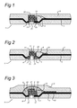
- a first embodiment of the package 1 according to the invention is shown in a cross sectional view.
- the package 1 comprises a carrier element 3 in the form of a lead frame carrier onto which a sensor assembly 2 is attached.
- the lead frame carrier 3 is used to provide the external electrical connections of the package 1, but in some packages also forms a supporting structure for the sensor assembly 2 (during production).
- the sensor assembly 2 is in this embodiment a sensor which requires to be exposed to the outside of the package 1, and e.g. comprises a micro electromechanical sensor (MEMS) such as a g-sensor or pressure sensor.
- MEMS micro electromechanical sensor
- the sensor sensitivity is important, as well as a number of other operational characteristics, such as hysteresis or stress induced errors. These operational characteristics are influenced by the manner in which the package 1 is assembled.
- the sensor assembly 2 comprises a sensitive surface 21 and, in the embodiment shown, two sensor attachment surfaces 22.
- the lead frame carrier 3 comprises two sensor attachment areas 31, to which the sensor attachment surfaces 22 are mounted using a sensor attach material 4.
- the sensor attach material 4 may e.g. be a low stress epoxy or a kind of gel (such as silicone gel).
- the sensor assembly 2 provides its signals to the lead frame carrier using electrical connections 6, e.g. wires as shown in this embodiment (using wire bonding).
- an encapsulation or enclosure 5 of a first ( duroplast) material is made, in which the encapsulation 5 covers at least the sensor attachment area 31 of the lead frame carrier 3 and the sensor attach material 4. Also, the electrical connections 6 are covered by the encapsulation 5.
- the sensitive surface 21 of the sensor assembly 2 and a surrounding area thereof are kept free from the duroplast material.
- a duroplast material is considered herein to be a composite thermosetting plastic. E.g., it is a resin plastic reinforced with fibres (either cotton or wool), making it a fibre-reinforced plastic similar to glass-reinforced plastic.
- the duroplast material is e.g. a moulding compound having low stress when being cured.
- a low stress duroplast material e.g. has a high filler amount, and a low thermal expansion above and below the glass temperature Tg.
- the lead frame carrier 3 is of a material which is chosen to have a thermal expansion coefficient which is in the same order of magnitude as the thermal expansion coefficient of the (cured) duroplast material of the encapsulation 5.
- the use of Alloy42 yields a better result than the conventional copper material.
- the lead frame carrier 3 might be formed by a plastic die-pad from duroplast or thermoplast material.
- the moulding compound shrinkage during curing may e.g. induce stress after assembly, and also differences in thermal expansion coefficients may induce stress related effects on the operational characteristics during operation. Even the sensor attach material 4 may influence operational characteristics, e.g. resulting in a hysteresis of the sensor output signal.
- the present embodiment it is possible to obtain a reliable package 1 which is able to withstand harsh environments, such as encountered in engine exhaust applications and other automotive applications. This is primarily due to the fact that only a small part of the sensor assembly 2 (sensitive surface 21 and small surrounding area) is exposed to the environment, and all other parts and elements in the package 1 are screened off from this environment.
- the sensitive surface 21 of the sensor assembly may also be provided at the top part of the sensor assembly 2, with a corresponding opening in the top part of the package 1.
- the package 1 may be provided with two openings, both at the top and bottom part, e.g. in case of the application of a differential sensor in the sensor assembly 2.
- the sensor assembly 2 may be provided with more than one sensitive surface 21, e.g. combining several sensors in one sensor assembly 2. The package 1 may then be provided with a single opening or multiple openings.
- the lead frame carrier 3 is provided with only one sensor attachment area 31 (and the sensor assembly 2 with only a single corresponding attachment surface 22).
- a further electronic component 10 e.g. an application specific integrated circuit (ASIC) is part of the package 1.
- the component 10 is attached to the lead frame carrier 3, and completely encapsulated with the duroplast material.
- the ASIC 10 may e.g. be provided to condition or pre-process the signal from the sensor assembly 2, via the electrical connection 6.
- the lead frame carrier 3 is provided with a separate element 7 attached or moulded to the lead frame carrier 3.
- the sensor attachment area 71 is then provided by this separate element 7.
- FIG. 3 An even further embodiment is schematically shown in Fig. 3 .
- an electronic component 10 is comprised in the package 1, connected to the sensor assembly 2 using a bonding wire 6.
- the lead frame carrier 3 can be provided with a recessed area including the sensor attachment areas 31.
- the sensor assembly 2 Prior to the duroplast material being inserted when moulding the encapsulation 5, the sensor assembly 2 is covered with a second material, e.g. a gel like material. As a result a cavity 8 is created above the sensor assembly 2, which is almost entirely filled with the gel like material. Due to the fact the expansion/shrinkage of the gel like material is significant higher compared to the thermoharder material of the encapsulation 5 a gap will be created after encapsulation.
- a second material e.g. a gel like material
- This gap decouples the sensor from the encapsulation (below a certain temperature, depending on the expansion factor of the gel like material).
- Proper selection of the second material may provide further benefits, e.g. shielding for electromagnetic compatibility (EMC) purposes.
- EMC electromagnetic compatibility
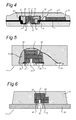
- Fig. 4 shows a schematic cross sectional view of an even further embodiment of the present invention.
- the separate attachment element 7 of the Fig. 2 embodiment is provided as a pre-moulded cavity 9.
- This premoulded cavity 9 may be of duroplast or thermoplast material, and includes a sensor attachment area 91.
- the premoulded cavity 9 may be provided with rims 92, thus forming the cavity 8 above the sensor assembly 2, which may be filled again with e.g. a gel like material.
- the cavity 8 is not filled with a gel like material, but left filled with surrounding air or a vacuum.
- an additional processing step is necessary, in which the cavity 8 is closed off before application (injection) of the duroplast material to form the encapsulation 5.
- packages 1 have been shown and described which are provided with a lead frame carrier 3.
- the present invention may also be applied in other types of packages 1, e.g. Quad Flat No Lead (QFN) packages 1, or Ball Grid Array (BGA) packages 1.
- QFN Quad Flat No Lead
- BGA Ball Grid Array
- FIG. 5 An embodiment of a QFN package 1 is shown in cross sectional view in Fig. 5 .
- the QFN package 1 comprises a number of connecting pads 35, of which one or more act as sensor attachment area for the sensor assembly 2.
- the connecting pads 35 are the functional equivalent of the lead frame carrier 3 as described above.
- the attachment surfaces 21 of the sensor assembly 2 are attached to the connecting pads 35 using an attachment material 4.
- the sensitive surface 21 and a small surrounding area of the sensor assembly are the only parts of the package 1 exposed to the environment.
- FIG. 6 An embodiment of a BGA package 1 is shown in cross sectional view in Fig. 6 .
- the BGA package 1 comprises a connecting board 36, and conductive balls 37.
- the conductive balls 37 act as electrical connections 6 to connect the sensor assembly 2 to the board 36, but also as attachment material (using soldering techniques). Again, when injecting the duroplast material for the encapsulation 5, the sensitive surface 21 and a small surrounding area of the sensor assembly are the only parts of the package 1 exposed to the environment.
Landscapes
- Physics & Mathematics (AREA)
- General Physics & Mathematics (AREA)
- Structures Or Materials For Encapsulating Or Coating Semiconductor Devices Or Solid State Devices (AREA)
- Pressure Sensors (AREA)
Priority Applications (2)
| Application Number | Priority Date | Filing Date | Title |
|---|---|---|---|
| EP08151407A EP2090873B1 (de) | 2008-02-14 | 2008-02-14 | Integriertes Schaltungsgehäuse |
| US12/369,959 US8049290B2 (en) | 2008-02-14 | 2009-02-12 | Integrated circuit package |
Applications Claiming Priority (1)
| Application Number | Priority Date | Filing Date | Title |
|---|---|---|---|
| EP08151407A EP2090873B1 (de) | 2008-02-14 | 2008-02-14 | Integriertes Schaltungsgehäuse |
Publications (2)
| Publication Number | Publication Date |
|---|---|
| EP2090873A1 true EP2090873A1 (de) | 2009-08-19 |
| EP2090873B1 EP2090873B1 (de) | 2011-06-01 |
Family
ID=39580613
Family Applications (1)
| Application Number | Title | Priority Date | Filing Date |
|---|---|---|---|
| EP08151407A Active EP2090873B1 (de) | 2008-02-14 | 2008-02-14 | Integriertes Schaltungsgehäuse |
Country Status (2)
| Country | Link |
|---|---|
| US (1) | US8049290B2 (de) |
| EP (1) | EP2090873B1 (de) |
Cited By (2)
| Publication number | Priority date | Publication date | Assignee | Title |
|---|---|---|---|---|
| WO2010072455A1 (de) | 2008-12-16 | 2010-07-01 | Robert Bosch Gmbh | Vorrichtung und verfahren zur herstellung einer vorrichtung |
| WO2015057058A2 (en) | 2013-10-18 | 2015-04-23 | Sencio B.V. | Integrated circuit package |
Families Citing this family (7)
| Publication number | Priority date | Publication date | Assignee | Title |
|---|---|---|---|---|
| PT105191A (pt) * | 2010-07-08 | 2012-01-09 | Fiorima Fabricacao De Peugas S A | Peúga para monitorização biométrica integrada |
| US8618620B2 (en) | 2010-07-13 | 2013-12-31 | Infineon Technologies Ag | Pressure sensor package systems and methods |
| US20120043628A1 (en) * | 2010-08-19 | 2012-02-23 | Avago Technologies Wireless Ip (Singapore) Pte. Ltd. | Packaged device including a well for containing a die |
| DE102014010116B4 (de) | 2013-04-29 | 2018-11-15 | Elmos Semiconductor Aktiengesellschaft | MEMS Sensor für schwierige Umgebungen und Medien |
| US9190352B2 (en) * | 2013-11-21 | 2015-11-17 | Freescale Semiconductor, Inc. | Multi-die sensor device |
| JP6520636B2 (ja) * | 2015-10-16 | 2019-05-29 | 株式会社デンソー | 物理量センササブアセンブリおよび物理量測定装置 |
| US9952110B2 (en) * | 2016-03-29 | 2018-04-24 | Infineon Technologies Ag | Multi-die pressure sensor package |
Citations (6)
| Publication number | Priority date | Publication date | Assignee | Title |
|---|---|---|---|---|
| US5207102A (en) * | 1991-02-12 | 1993-05-04 | Mitsubishi Denki Kabushiki Kaisha | Semiconductor pressure sensor |
| US6401545B1 (en) * | 2000-01-25 | 2002-06-11 | Motorola, Inc. | Micro electro-mechanical system sensor with selective encapsulation and method therefor |
| US6521966B1 (en) * | 1999-04-14 | 2003-02-18 | Denso Corporation | Semiconductor strain sensor |
| DE10316084A1 (de) * | 2002-11-11 | 2004-05-27 | Mitsubishi Denki K.K. | Halbleiterdrucksensor |
| WO2007017301A1 (de) | 2005-08-05 | 2007-02-15 | Robert Bosch Gmbh | Gemoldeter mikromechanischer kraft-/druckwandler sowie ein entsprechendes herstellungsverfahren |
| DE102005038443A1 (de) * | 2005-08-16 | 2007-02-22 | Robert Bosch Gmbh | Sensoranordnung mit einem Substrat und mit einem Gehäuse und Verfahren zur Herstellung einer Sensoranordnung |
Family Cites Families (3)
| Publication number | Priority date | Publication date | Assignee | Title |
|---|---|---|---|---|
| DE19929026B4 (de) * | 1999-06-25 | 2011-02-24 | Robert Bosch Gmbh | Verfahren zur Herstellung eines Drucksensors |
| DE102004027094A1 (de) * | 2004-06-02 | 2005-12-29 | Infineon Technologies Ag | Halbleitermodul mit einem Halbleiter-Sensorchip und einem Kunststoffgehäuse sowie Verfahren zu dessen Herstellung |
| CN100517738C (zh) * | 2005-07-15 | 2009-07-22 | 鸿富锦精密工业(深圳)有限公司 | 影像感测芯片的封装结构 |
-
2008
- 2008-02-14 EP EP08151407A patent/EP2090873B1/de active Active
-
2009
- 2009-02-12 US US12/369,959 patent/US8049290B2/en active Active
Patent Citations (6)
| Publication number | Priority date | Publication date | Assignee | Title |
|---|---|---|---|---|
| US5207102A (en) * | 1991-02-12 | 1993-05-04 | Mitsubishi Denki Kabushiki Kaisha | Semiconductor pressure sensor |
| US6521966B1 (en) * | 1999-04-14 | 2003-02-18 | Denso Corporation | Semiconductor strain sensor |
| US6401545B1 (en) * | 2000-01-25 | 2002-06-11 | Motorola, Inc. | Micro electro-mechanical system sensor with selective encapsulation and method therefor |
| DE10316084A1 (de) * | 2002-11-11 | 2004-05-27 | Mitsubishi Denki K.K. | Halbleiterdrucksensor |
| WO2007017301A1 (de) | 2005-08-05 | 2007-02-15 | Robert Bosch Gmbh | Gemoldeter mikromechanischer kraft-/druckwandler sowie ein entsprechendes herstellungsverfahren |
| DE102005038443A1 (de) * | 2005-08-16 | 2007-02-22 | Robert Bosch Gmbh | Sensoranordnung mit einem Substrat und mit einem Gehäuse und Verfahren zur Herstellung einer Sensoranordnung |
Non-Patent Citations (1)
| Title |
|---|
| COTOFANA C ET AL: "Low-cost plastic sensor packaging using the open-window package concept", SENSORS AND ACTUATORS A, ELSEVIER SEQUOIA S.A., LAUSANNE, CH, vol. 67, no. 1-3, 15 May 1998 (1998-05-15), pages 185 - 190, XP004130134, ISSN: 0924-4247 * |
Cited By (7)
| Publication number | Priority date | Publication date | Assignee | Title |
|---|---|---|---|---|
| WO2010072455A1 (de) | 2008-12-16 | 2010-07-01 | Robert Bosch Gmbh | Vorrichtung und verfahren zur herstellung einer vorrichtung |
| CN102257374A (zh) * | 2008-12-16 | 2011-11-23 | 罗伯特·博世有限公司 | 装置和用于制造装置的方法 |
| US20110290016A1 (en) * | 2008-12-16 | 2011-12-01 | Volker Dietrich | Device and method for producing a device |
| US8621925B2 (en) | 2008-12-16 | 2014-01-07 | Robert Bosch Gmbh | Device and method for producing a device |
| CN102257374B (zh) * | 2008-12-16 | 2014-12-24 | 罗伯特·博世有限公司 | 传感器装置和用于制造传感器装置的方法 |
| WO2015057058A2 (en) | 2013-10-18 | 2015-04-23 | Sencio B.V. | Integrated circuit package |
| US9754913B2 (en) | 2013-10-18 | 2017-09-05 | Sencio B.V. | Integrated circuit package |
Also Published As
| Publication number | Publication date |
|---|---|
| EP2090873B1 (de) | 2011-06-01 |
| US8049290B2 (en) | 2011-11-01 |
| US20090206467A1 (en) | 2009-08-20 |
Similar Documents
| Publication | Publication Date | Title |
|---|---|---|
| US8049290B2 (en) | Integrated circuit package | |
| JP5453310B2 (ja) | 圧力センサモジュール | |
| US8359927B2 (en) | Molded differential PRT pressure sensor | |
| US7900521B2 (en) | Exposed pad backside pressure sensor package | |
| US7216546B2 (en) | Pressure sensor having integrated temperature sensor | |
| US9952110B2 (en) | Multi-die pressure sensor package | |
| EP3176543B1 (de) | Leiterplattenmontagestruktur und sensor damit | |
| US20080026610A1 (en) | Sensor adaptor circuit housing assembly and method of manufacturing thereof | |
| US9841341B2 (en) | Package for semiconductor devices sensitive to mechanical and thermo-mechanical stresses, such as MEMS pressure sensors | |
| CN104254045A (zh) | 用于麦克风组件的预制模及其制造方法 | |
| JP2009505088A (ja) | 基板とケーシングとを備えたセンサ配置構造およびセンサ配置構造を製造する方法 | |
| JP5351943B2 (ja) | 両面センサパッケージとして使用される装置 | |
| CN104871308B (zh) | 用于制造电子组件的方法 | |
| US20200020616A1 (en) | Bottom package exposed die mems pressure sensor integrated circuit package design | |
| US7836764B2 (en) | Electrical device with covering | |
| US6313514B1 (en) | Pressure sensor component | |
| JP2000329632A (ja) | 圧力センサーモジュール及び圧力センサーモジュールの製造方法 | |
| JP4326609B2 (ja) | 半導体素子を製造する方法 | |
| CN111326420A (zh) | 模制引线框传感器封装 | |
| KR20190137699A (ko) | 압력 감지 애플리케이션들에 대한 오버몰딩된 리드 프레임 조립체 | |
| KR20150097630A (ko) | 측정 송신기의 제조 방법 | |
| US20170033034A1 (en) | Electronic device and package | |
| JP6317956B2 (ja) | 圧力センサ、及び圧力センサの製造方法 | |
| CN111458056B (zh) | 制造传感器设备和模制支撑结构的方法 | |
| GB2432457A (en) | Sensor arrangement and method for fabricating a sensor arrangement |
Legal Events
| Date | Code | Title | Description |
|---|---|---|---|
| PUAI | Public reference made under article 153(3) epc to a published international application that has entered the european phase |
Free format text: ORIGINAL CODE: 0009012 |
|
| AK | Designated contracting states |
Kind code of ref document: A1 Designated state(s): AT BE BG CH CY CZ DE DK EE ES FI FR GB GR HR HU IE IS IT LI LT LU LV MC MT NL NO PL PT RO SE SI SK TR |
|
| AX | Request for extension of the european patent |
Extension state: AL BA MK RS |
|
| 17P | Request for examination filed |
Effective date: 20100205 |
|
| 17Q | First examination report despatched |
Effective date: 20100310 |
|
| AKX | Designation fees paid |
Designated state(s): DE NL |
|
| GRAP | Despatch of communication of intention to grant a patent |
Free format text: ORIGINAL CODE: EPIDOSNIGR1 |
|
| GRAS | Grant fee paid |
Free format text: ORIGINAL CODE: EPIDOSNIGR3 |
|
| GRAA | (expected) grant |
Free format text: ORIGINAL CODE: 0009210 |
|
| AK | Designated contracting states |
Kind code of ref document: B1 Designated state(s): DE NL |
|
| REG | Reference to a national code |
Ref country code: DE Ref legal event code: R096 Ref document number: 602008007312 Country of ref document: DE Effective date: 20110714 |
|
| RAP2 | Party data changed (patent owner data changed or rights of a patent transferred) |
Owner name: SENCIO B.V. |
|
| REG | Reference to a national code |
Ref country code: NL Ref legal event code: T3 |
|
| PLBE | No opposition filed within time limit |
Free format text: ORIGINAL CODE: 0009261 |
|
| STAA | Information on the status of an ep patent application or granted ep patent |
Free format text: STATUS: NO OPPOSITION FILED WITHIN TIME LIMIT |
|
| 26N | No opposition filed |
Effective date: 20120302 |
|
| REG | Reference to a national code |
Ref country code: DE Ref legal event code: R097 Ref document number: 602008007312 Country of ref document: DE Effective date: 20120302 |
|
| REG | Reference to a national code |
Ref country code: NL Ref legal event code: SD Effective date: 20130201 |
|
| REG | Reference to a national code |
Ref country code: DE Ref legal event code: R081 Ref document number: 602008007312 Country of ref document: DE Owner name: SENCIO B.V., NL Free format text: FORMER OWNER: ELMOS ADVANCED PACKAGING B.V., NIJMEGEN, NL Effective date: 20130118 |
|
| REG | Reference to a national code |
Ref country code: NL Ref legal event code: PD Owner name: NEWAYS ADVANCED MICROSYSTEMS B.V.; NL Free format text: DETAILS ASSIGNMENT: CHANGE OF OWNER(S), ASSIGNMENT; FORMER OWNER NAME: SENCIO B.V. Effective date: 20241004 |
|
| REG | Reference to a national code |
Ref country code: DE Ref legal event code: R081 Ref document number: 602008007312 Country of ref document: DE Owner name: NEWAYS ADVANCED MICROSYSTEMS B.V., NL Free format text: FORMER OWNER: SENCIO B.V., NIJMEGEN, NL |
|
| PGFP | Annual fee paid to national office [announced via postgrant information from national office to epo] |
Ref country code: NL Payment date: 20251127 Year of fee payment: 19 |
|
| PGFP | Annual fee paid to national office [announced via postgrant information from national office to epo] |
Ref country code: DE Payment date: 20260220 Year of fee payment: 19 |