EP2091076A2 - Implantations de carbone pour améliorer la production de transistors bipolaires en SiGe - Google Patents
Implantations de carbone pour améliorer la production de transistors bipolaires en SiGe Download PDFInfo
- Publication number
- EP2091076A2 EP2091076A2 EP09162231A EP09162231A EP2091076A2 EP 2091076 A2 EP2091076 A2 EP 2091076A2 EP 09162231 A EP09162231 A EP 09162231A EP 09162231 A EP09162231 A EP 09162231A EP 2091076 A2 EP2091076 A2 EP 2091076A2
- Authority
- EP
- European Patent Office
- Prior art keywords
- region
- sige
- collector
- base
- regions
- Prior art date
- Legal status (The legal status is an assumption and is not a legal conclusion. Google has not performed a legal analysis and makes no representation as to the accuracy of the status listed.)
- Withdrawn
Links
Images
Classifications
-
- H—ELECTRICITY
- H10—SEMICONDUCTOR DEVICES; ELECTRIC SOLID-STATE DEVICES NOT OTHERWISE PROVIDED FOR
- H10D—INORGANIC ELECTRIC SEMICONDUCTOR DEVICES
- H10D10/00—Bipolar junction transistors [BJT]
- H10D10/80—Heterojunction BJTs
-
- H—ELECTRICITY
- H10—SEMICONDUCTOR DEVICES; ELECTRIC SOLID-STATE DEVICES NOT OTHERWISE PROVIDED FOR
- H10P—GENERIC PROCESSES OR APPARATUS FOR THE MANUFACTURE OR TREATMENT OF DEVICES COVERED BY CLASS H10
- H10P30/00—Ion implantation into wafers, substrates or parts of devices
- H10P30/20—Ion implantation into wafers, substrates or parts of devices into semiconductor materials, e.g. for doping
- H10P30/202—Ion implantation into wafers, substrates or parts of devices into semiconductor materials, e.g. for doping characterised by the semiconductor materials
- H10P30/204—Ion implantation into wafers, substrates or parts of devices into semiconductor materials, e.g. for doping characterised by the semiconductor materials into Group IV semiconductors
-
- H—ELECTRICITY
- H10—SEMICONDUCTOR DEVICES; ELECTRIC SOLID-STATE DEVICES NOT OTHERWISE PROVIDED FOR
- H10D—INORGANIC ELECTRIC SEMICONDUCTOR DEVICES
- H10D10/00—Bipolar junction transistors [BJT]
- H10D10/01—Manufacture or treatment
- H10D10/021—Manufacture or treatment of heterojunction BJTs [HBT]
-
- H—ELECTRICITY
- H10—SEMICONDUCTOR DEVICES; ELECTRIC SOLID-STATE DEVICES NOT OTHERWISE PROVIDED FOR
- H10D—INORGANIC ELECTRIC SEMICONDUCTOR DEVICES
- H10D10/00—Bipolar junction transistors [BJT]
- H10D10/80—Heterojunction BJTs
- H10D10/821—Vertical heterojunction BJTs
- H10D10/891—Vertical heterojunction BJTs comprising lattice-mismatched active layers, e.g. SiGe strained-layer transistors
-
- H—ELECTRICITY
- H10—SEMICONDUCTOR DEVICES; ELECTRIC SOLID-STATE DEVICES NOT OTHERWISE PROVIDED FOR
- H10D—INORGANIC ELECTRIC SEMICONDUCTOR DEVICES
- H10D62/00—Semiconductor bodies, or regions thereof, of devices having potential barriers
- H10D62/10—Shapes, relative sizes or dispositions of the regions of the semiconductor bodies; Shapes of the semiconductor bodies
- H10D62/17—Semiconductor regions connected to electrodes not carrying current to be rectified, amplified or switched, e.g. channel regions
- H10D62/177—Base regions of bipolar transistors, e.g. BJTs or IGBTs
-
- H—ELECTRICITY
- H10—SEMICONDUCTOR DEVICES; ELECTRIC SOLID-STATE DEVICES NOT OTHERWISE PROVIDED FOR
- H10D—INORGANIC ELECTRIC SEMICONDUCTOR DEVICES
- H10D62/00—Semiconductor bodies, or regions thereof, of devices having potential barriers
- H10D62/10—Shapes, relative sizes or dispositions of the regions of the semiconductor bodies; Shapes of the semiconductor bodies
- H10D62/17—Semiconductor regions connected to electrodes not carrying current to be rectified, amplified or switched, e.g. channel regions
- H10D62/192—Base regions of thyristors
-
- H—ELECTRICITY
- H10—SEMICONDUCTOR DEVICES; ELECTRIC SOLID-STATE DEVICES NOT OTHERWISE PROVIDED FOR
- H10P—GENERIC PROCESSES OR APPARATUS FOR THE MANUFACTURE OR TREATMENT OF DEVICES COVERED BY CLASS H10
- H10P30/00—Ion implantation into wafers, substrates or parts of devices
- H10P30/20—Ion implantation into wafers, substrates or parts of devices into semiconductor materials, e.g. for doping
- H10P30/208—Ion implantation into wafers, substrates or parts of devices into semiconductor materials, e.g. for doping of electrically inactive species
Definitions
- the present invention relates to semiconductor heterojunction bipolar transistors, and more particularly to a method of fabricating a SiGe heterojunction bipolar transistor in which the SiGe bipolar yield is substantially improved by suppressing dislocations that cause collector-emitter (CE) leakage or shorts, or collector-base (CB) leakage or shorts.
- CE collector-emitter
- CB collector-base
- CMOS complementary metal oxide semiconductor
- bipolar pipe shorts i.e., collector-emitter shorts
- SiGe bipolar yield can be reduced by as much as 20 to 50% for dislocations originating in the collector region.
- One object of the present invention is to provide a method of fabricating a SiGe heterojunction bipolar transistor wherein improved SiGe bipolar yield is achieved.
- Another object of the present invention is to provide a method of fabricating a SiGe heterojunction bipolar transistor in which the amount of dislocations present in the device is substantially reduced thereby avoiding pipe shorts.
- a further object of the present invention is to provide a method of fabricating a SiGe heterojunction bipolar transistor using processing steps that are compatible with existing bipolar and CMOS processing steps.
- the greatest enhancement and most preferred embodiment of the present invention is obtained when all the C implants, as defined hereinabove, are employed.
- the improved SiGe bipolar yield obtained by the present invention is a significant advancement in this art since it results in a device having substantially less pipe shorts than heretofore possible with prior art SiGe heterojunction bipolar devices.
- the present invention includes a method for improving the SiGe bipolar yield which comprises the steps of:
- the SiGe layer is grown utilizing a non-selective epi process.
- the SiGe layer would include extrinsic base regions abutting the intrinsic base region.
- the SiGe layer is formed without extrinsic base regions.
- the extrinsic base regions which may or may not include germanium, are formed separately from the SiGe layer.
- the method of the present invention comprises the steps of:
- a further aspect of the present invention relates to a SiGe heterojunction bipolar transistor that has improved SiGe bipolar yield.
- the inventive SiGe heterojunction bipolar transistor comprises:
- the bipolar transistor comprises:
- each of the C-doped regions is formed by implanting C into the specific region by utilizing the method of the present invention.
- FIGS 1-7 The present invention which is related to the use of C implants for improving SiGe bipolar yield will now be described in more detail by referring to FIGS 1-7 and the discussion that appears hereinbelow. It is noted that in the drawings like and corresponding elements are referred to by like reference numerals. Also, for simplicity, only one bipolar device region is shown in the drawings. Other bipolar device regions as well as digital logic circuitry may be formed adjacent to the bipolar device region depicted in the drawings.
- the drawings depict the preferred embodiment of the invention wherein the SiGe layer is formed with extrinsic base regions abutting the intrinsic base regions.
- the extrinsic base regions are formed by a non-selective epi deposition process.
- the present invention also contemplates SiGe layers in which the extrinsic base regions are formed separately from the SiGe layer.
- implantation of C occurs in all four regions, i.e., the collector, sub-collector, extrinsic base regions and said collector-base junction region. Such C implantation into all four regions represents the most preferred embodiment of the present invention.
- the present invention is however not limited to C implants into each of these four regions. Instead, in the present invention, at least one of the regions must include C implants.
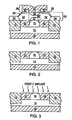
- FIG 1 represents a cross-sectional view of the inventive SiGe heterojunction bipolar transistor.
- the SiGe heterojunction bipolar transistor comprises semiconductor substrate 10 of a first conductivity type (N or P), sub-collector region 14 and collector region 16 which are both doped with C via implantation.
- Isolation regions 12 which are also present in the structure define the outer boundaries of the bipolar device region and serve to isolate the bipolar device region shown in FIG 1 from adjacent device regions (not shown).
- the SiGe bipolar transistor of FIG 1 also includes SiGe base layer 20 formed on substrate 10 as well as on isolation regions 12.
- the SiGe base layer includes polycrystalline Si regions 24 that are formed predominately over isolation regions 12, and single-crystal SiGe region 22, which includes extrinsic SiGe base regions 29, intrinsic SiGe base region 26, and collector-base junction region 27, also referred to in the art as the pedestal region of the device, formed predominately over sub-collector region 14.
- the collector-base junction region, and the extrinsic base regions are both doped with C via implantation. Note that the solid line separating each polycrystalline SiGe region from the single-crystal SiGe region is referred to in the art as a facet region.
- the bipolar transistor of FIG 1 also comprises emitter region 28 which includes patterned insulator layer 30 which has an emitter opening formed therein and a region of emitter polysilicon 32 formed on said patterned insulator layer as well as in said emitter opening.
- the emitter polysilicon is typically doped N+. Note that after formation of the emitter polysilicon, dopant from the emitter polysilicon is diffused into the intrinsic base region forming emitter diffusion region 34 in the intrinsic base region 26.
- the bipolar transistor shown in FIG 1 has improved SiGe bipolar yield because the C implants in the above identified regions, i.e., sub-collector, collector, extrinsic base and/or collector-base junction region, reduce the number of dislocations that are present in the structure.
- improved bipolar yield i.e., emitter-base or emitter-collector leakage yield
- emitter-base or emitter-collector leakage yield when at least one of the above-mentioned regions is doped with C implants; however the greatest affect is observed when all the regions include C implants.
- bipolar yield may be improved as much as 20 to 50%; therefore the present invention provides an improved structure compared with prior art SiGe bipolar transistors which do not contain C implants in the collector, sub-collector, extrinsic base regions and/or the collector-base junction region.
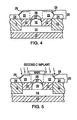
- FIG 2 shows the bipolar device region of an initial structure that is employed in the present invention.
- the initial structure shown in FIG 2 comprises substrate 10 having sub-collector region 14, collector region 16 and isolation regions 12 formed therein.
- substrate 10 is composed of any semiconducting material including but not limited to: Si, Ge, SiGe, GaAs, InAs, InP and all other III/V compound semiconductors. Layered substrates comprising the same or different semiconducting material, e.g., Si/Si or Si/SiGe, are also contemplated herein. Of these semiconducting materials, it is preferred that substrate 10 be composed of Si. As mentioned above, the substrate may be a N-type substrate or a P-type substrate depending on the type of device to be subsequently formed.
- Sub-collector region 14 is formed in, or alternatively on the substrate by using any well known technique that is capable of forming a sub-collector region in such a structure.
- the sub-collector region can be formed via implantation or by an epitaxial growth process.
- Isolations regions 12 are then formed by either using a conventional local oxidation of silicon (LOCOS) process or by utilizing lithography, etching and trench isolation filling.
- LOCS local oxidation of silicon
- collector region 16 is then formed in the bipolar device region (between the two isolation regions shown in FIG 1 ) utilizing conventional ion implantation and activating annealing processes that are well known to those skilled in the art.
- the activating annealing process is typically carried out at a temperature of about 950°C or above for a time of about 30 seconds or less.
- the bipolar device region shown in the drawings may be protected by forming a protective material such as Si 3 N 4 thereon, and conventional processing steps which are capable of forming adjacent device regions can be performed. After completion of the adjacent device regions and subsequent protection thereof, the inventive process continues. It should be noted that in some embodiments, the adjacent device regions are formed after completely fabricating the bipolar transistor.
- FIG 3 shows the ion implantation of C into sub-collector region 14 and collector region 16.
- the source of carbon used for implanting these regions is a C-containing material such as CO 2 or any other C-containing gas source.
- This first C implantation step which may be carried out utilizing a one or two-step process is carried out using a C dose of from about 1E13 to about 1E16 cm -2 .
- An implantation energy of from about 5 to about 200 keV is employed for implanting C into the collector region, whereas an energy of from about 10 to about 1000 keV is employed for implanting C into the sub-collector region.
- this first C implantation step is carried out using a C dose of about 1 E14 cm -2 and an implantation energy of about 20 keV for the collector region and about 400 keV for the sub-collector region.
- the C source may be used neat (i.e., non-mixed), or it may be mixed with an inert gas such as He or Ar. These implants may be blanket or masked using techniques well known to those skilled in the art. In some embodiments, it is possible to omit implanting C into the collector and subcollector regions.
- the C implant into the sub-collector region may occur during formation of the isolation regions or may occur after formation of the isolation regions, as is shown herein.
- the collector region is typically implanted with C after the adjacent devices have been formed and protected.
- the first C implant step mentioned above allows for a carbon source to be present in the structure that will reduce the level of free interstitials forming dislocations at the base of the SiGe layer.
- the mechanism of reduction of interstitial levels due to C implant is believed to be as follows: C in substitutional or interstitial positions reacts with interstitial Si atoms. The C-Si pairs are either complexed with other C atoms or diffuse out from the high concentration interstitial region. This causes a reduction in the overall concentration of interstitials thereby reducing the level of dislocations that may be formed.
- C implantation into the sub-collector region typically occurs prior to C implantation into the collector region.
- SiGe layer 20 is formed on substrate 10 as well as on isolation regions 12.
- the SiGe layer includes polycrystalline Si regions 24 that are formed predominately over isolation regions 12, and single-crystal SiGe layer 22 that is formed predominately over the sub-collector region.
- the single-crystal SiGe region further includes extrinsic SiGe base regions 29 and intrinsic SiGe base region 26.
- the extrinsic base region is an implanted region which can be formed by either a blanket ion implantation process or a combined patterning/ion implantation process.
- the SiGe layer is formed epitaxially utilizing a well-known deposition process including, but not limited to: ultra-high vacuum chemical vapor deposition (UHVCVD) and rapid thermal chemical vapor deposition (RTCVP).
- UHVCVD ultra-high vacuum chemical vapor deposition
- RTCVP rapid thermal chemical vapor deposition
- the present invention is not limited to the embodiment wherein the SiGe layer is formed by epitaxial deposition. Note that when epi processes are employed the SiGe layer is formed with extrinsic base regions abutting the intrinsic base region. The present invention also contemplates cases wherein the extrinsic base regions are formed during the deposition of the SiGe layer utilizing the processes mentioned above.
- a second C implantation step is performed. Specifically, it has been determined that C implantation into both the extrinsic base regions and the collector-base junction region reduces the level of dislocations present in the structure.
- the second C implantation step which implants C into the extrinsic SiGe base regions is carried out using a C dose of from about 1 E13 to about 1 E16 cm -2 and an implantation energy of from about 5 to about 200 keV. More preferably, the second C implantation step is carried out using a C dose of about 1 E14 cm -2 and an implantation energy of about 15 keV.
- the same or different C source as used in the first C implantation step may be used in the second carbon implantation step. Note that in some embodiments, the second implant step, i.e., C implant into the extrinsic base regions, may be omitted.
- An N-type dopant implant may optionally be carried out in the pedestal, i.e., collector-base junction region 27, and/or collector region 16 at this point of the inventive method so as to form a device which operates at high-speeds.
- the optional N-type dopant implant is carried out using conventional processing techniques that are well known to those skilled in the art including, for example, ion implantation and activation annealing. It is noted that during this implant step, dislocations may also form in the structure causing shorts due to implantation damage caused by the implant. The region where this occurs in is typically just below the intrinsic SiGe base region.
- an insulator layer 30 is formed on SiGe base layer 20 utilizing a conventional deposition process such as CVD, plasma-assisted CVD, chemical solution deposition and other like deposition processes.
- the insulator may be a single layer, as is shown in FIG 6 , or it may contain multi-insulator layers.
- Insulator layer 30 is composed of the same or different insulator material which is selected from the group consisting of SiO 2 , Si oxynitride and other like insulators.
- Emitter opening 31 is then formed in insulator layer 30 so as to expose a portion of the intrinsic base region, See FIG 7 .
- the emitter opening is formed utilizing lithography and etching.
- the etching step used is selective in removing the insulator material as compared to the SiGe layer.
- C may be implanted into collector-base junction region 27, also referred to in the art as a pedestal region of the device, using a third C ion implantation process that is carried out using a C dose of from about 1 E 13 to about 1 E 16 cm -2 and at an energy of from about 5 to about 200 keV. More preferably, the third C.
- the implant is carried out at a C dose of about 1E14cm -2 and an energy of about 50 keV.
- the third C implant step includes the use of the same or different C source as the first C implant step and that in some embodiments the third implant may be omitted.
- emitter polysilicon layer 32 is formed on the insulator layer and in the emitter opening by utilizing a conventional deposition process such as CVD.
- the emitter polysilicon and the insulator are then selectively removed so as to form emitter region 28 on the SiGe base region, See FIG 1 .
- lithography and etching are employed in forming the structure shown in FIG 1 . It is should be noted that a single etching process may be employed in removing portions of emitter polysilicon layer 32 and insulator layer 30, or separate etching steps may be employed in removing these layers.
- emitter diffusion region 34 is formed in the intrinsic base region 26 during a subsequent annealing step.
Landscapes
- Bipolar Transistors (AREA)
- Bipolar Integrated Circuits (AREA)
Applications Claiming Priority (2)
| Application Number | Priority Date | Filing Date | Title |
|---|---|---|---|
| US09/878,605 US6534371B2 (en) | 2001-06-11 | 2001-06-11 | C implants for improved SiGe bipolar yield |
| EP02754741A EP1396018B8 (fr) | 2001-06-11 | 2002-06-04 | Implantations de carbone pour l'amelioration de la capacite de transistors dipolaires sige |
Related Parent Applications (1)
| Application Number | Title | Priority Date | Filing Date |
|---|---|---|---|
| EP02754741A Division EP1396018B8 (fr) | 2001-06-11 | 2002-06-04 | Implantations de carbone pour l'amelioration de la capacite de transistors dipolaires sige |
Publications (2)
| Publication Number | Publication Date |
|---|---|
| EP2091076A2 true EP2091076A2 (fr) | 2009-08-19 |
| EP2091076A3 EP2091076A3 (fr) | 2009-09-16 |
Family
ID=25372373
Family Applications (2)
| Application Number | Title | Priority Date | Filing Date |
|---|---|---|---|
| EP09162231A Withdrawn EP2091076A3 (fr) | 2001-06-11 | 2002-06-04 | Implantations de carbone pour améliorer la production de transistors bipolaires en SiGe |
| EP02754741A Expired - Lifetime EP1396018B8 (fr) | 2001-06-11 | 2002-06-04 | Implantations de carbone pour l'amelioration de la capacite de transistors dipolaires sige |
Family Applications After (1)
| Application Number | Title | Priority Date | Filing Date |
|---|---|---|---|
| EP02754741A Expired - Lifetime EP1396018B8 (fr) | 2001-06-11 | 2002-06-04 | Implantations de carbone pour l'amelioration de la capacite de transistors dipolaires sige |
Country Status (10)
| Country | Link |
|---|---|
| US (3) | US6534371B2 (fr) |
| EP (2) | EP2091076A3 (fr) |
| JP (2) | JP4086778B2 (fr) |
| KR (1) | KR100615789B1 (fr) |
| CN (1) | CN100459071C (fr) |
| AT (1) | ATE439682T1 (fr) |
| DE (1) | DE60233319D1 (fr) |
| MY (1) | MY134124A (fr) |
| TW (1) | TWI222142B (fr) |
| WO (1) | WO2002101810A1 (fr) |
Families Citing this family (27)
| Publication number | Priority date | Publication date | Assignee | Title |
|---|---|---|---|---|
| US6426265B1 (en) * | 2001-01-30 | 2002-07-30 | International Business Machines Corporation | Incorporation of carbon in silicon/silicon germanium epitaxial layer to enhance yield for Si-Ge bipolar technology |
| US6534371B2 (en) * | 2001-06-11 | 2003-03-18 | International Business Machines Corporation | C implants for improved SiGe bipolar yield |
| US20030082882A1 (en) * | 2001-10-31 | 2003-05-01 | Babcock Jeffrey A. | Control of dopant diffusion from buried layers in bipolar integrated circuits |
| US20050250289A1 (en) * | 2002-10-30 | 2005-11-10 | Babcock Jeffrey A | Control of dopant diffusion from buried layers in bipolar integrated circuits |
| US6670654B2 (en) * | 2002-01-09 | 2003-12-30 | International Business Machines Corporation | Silicon germanium heterojunction bipolar transistor with carbon incorporation |
| US6699765B1 (en) * | 2002-08-29 | 2004-03-02 | Micrel, Inc. | Method of fabricating a bipolar transistor using selective epitaxially grown SiGe base layer |
| US6972441B2 (en) * | 2002-11-27 | 2005-12-06 | Intel Corporation | Silicon germanium heterojunction bipolar transistor with step-up carbon profile |
| FR2852262B1 (fr) * | 2003-03-11 | 2007-01-12 | Procede et dispositif de nebulisation. | |
| DE10316531A1 (de) * | 2003-04-10 | 2004-07-08 | Infineon Technologies Ag | Bipolar-Transistor |
| JP3653087B2 (ja) | 2003-07-04 | 2005-05-25 | 三菱重工業株式会社 | Dc/dcコンバータ |
| US7005359B2 (en) * | 2003-11-17 | 2006-02-28 | Intel Corporation | Bipolar junction transistor with improved extrinsic base region and method of fabrication |
| DE102004021241A1 (de) * | 2004-04-30 | 2005-11-17 | Infineon Technologies Ag | Verfahren zur Herstellung eines planaren Spacers, eines zugehörigen Bipolartransistors und einer zugehörigen BiCMOS-Schaltungsanordnung |
| US7118995B2 (en) * | 2004-05-19 | 2006-10-10 | International Business Machines Corporation | Yield improvement in silicon-germanium epitaxial growth |
| US7655529B1 (en) * | 2004-08-20 | 2010-02-02 | Hrl Laboratories, Llc | InP based heterojunction bipolar transistors with emitter-up and emitter-down profiles on a common wafer |
| US7170083B2 (en) * | 2005-01-07 | 2007-01-30 | International Business Machines Corporation | Bipolar transistor with collector having an epitaxial Si:C region |
| US7144787B2 (en) * | 2005-05-09 | 2006-12-05 | International Business Machines Corporation | Methods to improve the SiGe heterojunction bipolar device performance |
| US7892915B1 (en) * | 2006-03-02 | 2011-02-22 | National Semiconductor Corporation | High performance SiGe:C HBT with phosphorous atomic layer doping |
| CN101937846B (zh) * | 2010-09-10 | 2015-10-21 | 上海华虹宏力半导体制造有限公司 | SiGe HBT晶体管及其制造方法 |
| US8728897B2 (en) | 2012-01-03 | 2014-05-20 | International Business Machines Corporation | Power sige heterojunction bipolar transistor (HBT) with improved drive current by strain compensation |
| US9105570B2 (en) * | 2012-07-13 | 2015-08-11 | Taiwan Semiconductor Manufacturing Company, Ltd. | Methods for introducing carbon to a semiconductor structure |
| US9064796B2 (en) | 2012-08-13 | 2015-06-23 | Infineon Technologies Ag | Semiconductor device and method of making the same |
| US9209264B2 (en) * | 2013-03-12 | 2015-12-08 | Newport Fab, Llc | Heterojunction bipolar transistor having a germanium raised extrinsic base |
| US9064886B2 (en) * | 2013-03-12 | 2015-06-23 | Newport Fab, Llc | Heterojunction bipolar transistor having a germanium extrinsic base utilizing a sacrificial emitter post |
| US9530708B1 (en) | 2013-05-31 | 2016-12-27 | Hrl Laboratories, Llc | Flexible electronic circuit and method for manufacturing same |
| FR3078197B1 (fr) * | 2018-02-21 | 2020-03-13 | Stmicroelectronics (Crolles 2) Sas | Dispositif de transistor bipolaire et procede de fabrication correspondant |
| US10784257B2 (en) | 2018-08-31 | 2020-09-22 | Nxp B.V. | Integrating silicon-BJT to a silicon-germanium-HBT manufacturing process |
| US11437486B2 (en) | 2020-01-14 | 2022-09-06 | Atomera Incorporated | Methods for making bipolar junction transistors including emitter-base and base-collector superlattices |
Citations (1)
| Publication number | Priority date | Publication date | Assignee | Title |
|---|---|---|---|---|
| FR2799049A1 (fr) | 1999-09-29 | 2001-03-30 | France Telecom | Procede pour empecher la diffusion de bore dans un silicium par implantation ionique de carbone |
Family Cites Families (24)
| Publication number | Priority date | Publication date | Assignee | Title |
|---|---|---|---|---|
| JPH03209833A (ja) * | 1989-12-01 | 1991-09-12 | Hewlett Packard Co <Hp> | 先進的エピタキシャル堆積技術を利用したSi/SiGe異種接合バイポーラトランジスタ及びその製造方法 |
| JPH05144834A (ja) | 1991-03-20 | 1993-06-11 | Hitachi Ltd | バイポーラトランジスタ及びその製造方法 |
| JPH05182980A (ja) * | 1992-01-07 | 1993-07-23 | Toshiba Corp | ヘテロ接合バイポーラトランジスタ |
| JPH05259178A (ja) * | 1992-03-16 | 1993-10-08 | Fujitsu Ltd | 半導体装置及びその製造方法 |
| JPH05267311A (ja) * | 1992-03-19 | 1993-10-15 | Toshiba Corp | バイポ−ラトランジスタ |
| US5372952A (en) | 1992-04-03 | 1994-12-13 | National Semiconductor Corporation | Method for forming isolated semiconductor structures |
| US5360986A (en) | 1993-10-05 | 1994-11-01 | Motorola, Inc. | Carbon doped silicon semiconductor device having a narrowed bandgap characteristic and method |
| EP0717435A1 (fr) | 1994-12-01 | 1996-06-19 | AT&T Corp. | Procédé de contrÔle de la diffusion de dopant dans une couche semiconductrice et couche semiconductrice ainsi formée |
| JPH09283533A (ja) * | 1996-04-15 | 1997-10-31 | Matsushita Electric Ind Co Ltd | ヘテロ接合バイポーラトランジスタ |
| US5753560A (en) | 1996-10-31 | 1998-05-19 | Motorola, Inc. | Method for fabricating a semiconductor device using lateral gettering |
| US6800881B2 (en) * | 1996-12-09 | 2004-10-05 | Ihp Gmbh-Innovations For High Performance Microelectronics/Institut Fur Innovative Mikroelektronik | Silicon-germanium hetero bipolar transistor with T-shaped implantation layer between emitter and emitter contact area |
| DE19755979A1 (de) * | 1996-12-09 | 1999-06-10 | Inst Halbleiterphysik Gmbh | Silizium-Germanium-Heterobipolartransistor |
| US6093613A (en) | 1998-02-09 | 2000-07-25 | Chartered Semiconductor Manufacturing, Ltd | Method for making high gain lateral PNP and NPN bipolar transistor compatible with CMOS for making BICMOS circuits |
| JP3201993B2 (ja) * | 1998-04-28 | 2001-08-27 | 松下電器産業株式会社 | 半導体装置とその製造方法 |
| JP3549408B2 (ja) * | 1998-09-03 | 2004-08-04 | 松下電器産業株式会社 | バイポーラトランジスタ |
| JP3515944B2 (ja) * | 1999-06-22 | 2004-04-05 | 松下電器産業株式会社 | ヘテロバイポーラトランジスタ |
| DE60042045D1 (de) * | 1999-06-22 | 2009-06-04 | Panasonic Corp | Heteroübergangsbipolartransistoren und entsprechende Herstellungsverfahren |
| JP2001035858A (ja) * | 1999-07-21 | 2001-02-09 | Matsushita Electric Ind Co Ltd | 半導体装置及びその製造方法 |
| FR2804247B1 (fr) * | 2000-01-21 | 2002-04-12 | St Microelectronics Sa | Procede de realisation d'un transistor bipolaire a emetteur et base extrinseque auto-alignes |
| US6316795B1 (en) * | 2000-04-03 | 2001-11-13 | Hrl Laboratories, Llc | Silicon-carbon emitter for silicon-germanium heterojunction bipolar transistors |
| FR2813707B1 (fr) * | 2000-09-07 | 2002-11-29 | St Microelectronics Sa | Fabrication d'un transistor bipolaire |
| US6426265B1 (en) * | 2001-01-30 | 2002-07-30 | International Business Machines Corporation | Incorporation of carbon in silicon/silicon germanium epitaxial layer to enhance yield for Si-Ge bipolar technology |
| US6750119B2 (en) * | 2001-04-20 | 2004-06-15 | International Business Machines Corporation | Epitaxial and polycrystalline growth of Si1-x-yGexCy and Si1-yCy alloy layers on Si by UHV-CVD |
| US6534371B2 (en) * | 2001-06-11 | 2003-03-18 | International Business Machines Corporation | C implants for improved SiGe bipolar yield |
-
2001
- 2001-06-11 US US09/878,605 patent/US6534371B2/en not_active Expired - Lifetime
-
2002
- 2002-05-09 MY MYPI20021676A patent/MY134124A/en unknown
- 2002-06-04 EP EP09162231A patent/EP2091076A3/fr not_active Withdrawn
- 2002-06-04 EP EP02754741A patent/EP1396018B8/fr not_active Expired - Lifetime
- 2002-06-04 AT AT02754741T patent/ATE439682T1/de not_active IP Right Cessation
- 2002-06-04 KR KR1020037014610A patent/KR100615789B1/ko not_active Expired - Fee Related
- 2002-06-04 WO PCT/EP2002/006923 patent/WO2002101810A1/fr not_active Ceased
- 2002-06-04 JP JP2003504456A patent/JP4086778B2/ja not_active Expired - Fee Related
- 2002-06-04 CN CNB028116461A patent/CN100459071C/zh not_active Expired - Lifetime
- 2002-06-04 DE DE60233319T patent/DE60233319D1/de not_active Expired - Lifetime
- 2002-06-10 TW TW091112545A patent/TWI222142B/zh not_active IP Right Cessation
-
2003
- 2003-01-08 US US10/338,476 patent/US6720590B2/en not_active Expired - Lifetime
-
2004
- 2004-04-07 US US10/819,732 patent/US6977398B2/en not_active Expired - Lifetime
-
2008
- 2008-01-16 JP JP2008006982A patent/JP5166046B2/ja not_active Expired - Fee Related
Patent Citations (1)
| Publication number | Priority date | Publication date | Assignee | Title |
|---|---|---|---|---|
| FR2799049A1 (fr) | 1999-09-29 | 2001-03-30 | France Telecom | Procede pour empecher la diffusion de bore dans un silicium par implantation ionique de carbone |
Also Published As
| Publication number | Publication date |
|---|---|
| JP2008135775A (ja) | 2008-06-12 |
| US20020185708A1 (en) | 2002-12-12 |
| US20030136975A1 (en) | 2003-07-24 |
| JP4086778B2 (ja) | 2008-05-14 |
| WO2002101810A1 (fr) | 2002-12-19 |
| JP2004532531A (ja) | 2004-10-21 |
| US6720590B2 (en) | 2004-04-13 |
| US6977398B2 (en) | 2005-12-20 |
| US6534371B2 (en) | 2003-03-18 |
| CN100459071C (zh) | 2009-02-04 |
| TWI222142B (en) | 2004-10-11 |
| EP1396018B1 (fr) | 2009-08-12 |
| JP5166046B2 (ja) | 2013-03-21 |
| ATE439682T1 (de) | 2009-08-15 |
| DE60233319D1 (de) | 2009-09-24 |
| US20040188711A1 (en) | 2004-09-30 |
| KR100615789B1 (ko) | 2006-08-25 |
| EP1396018B8 (fr) | 2009-12-16 |
| KR20040005955A (ko) | 2004-01-16 |
| EP2091076A3 (fr) | 2009-09-16 |
| MY134124A (en) | 2007-11-30 |
| CN1723550A (zh) | 2006-01-18 |
| EP1396018A1 (fr) | 2004-03-10 |
Similar Documents
| Publication | Publication Date | Title |
|---|---|---|
| EP1396018B1 (fr) | Implantations de carbone pour l'amelioration de la capacite de transistors dipolaires sige | |
| JP4917051B2 (ja) | シリコン・ゲルマニウム・バイポーラ・トランジスタの製造方法 | |
| US6177717B1 (en) | Low-noise vertical bipolar transistor and corresponding fabrication process | |
| JP2778553B2 (ja) | 半導体装置およびその製造方法 | |
| JPH11354537A (ja) | エピタキシャルベ―スをもつたて形バイポ―ラトランジスタの真性コレクタの選択ド―ピングを行う方法 | |
| US7538004B2 (en) | Method of fabrication for SiGe heterojunction bipolar transistor (HBT) | |
| US7476914B2 (en) | Methods to improve the SiGe heterojunction bipolar device performance | |
| US6913981B2 (en) | Method of fabricating a bipolar transistor using selective epitaxially grown SiGe base layer | |
| US5177025A (en) | Method of fabricating an ultra-thin active region for high speed semiconductor devices | |
| US6861324B2 (en) | Method of forming a super self-aligned hetero-junction bipolar transistor | |
| US6642096B2 (en) | Bipolar transistor manufacturing | |
| US20040201039A1 (en) | Silicon-germanium mesa transistor | |
| US7618871B2 (en) | Method for the production of a bipolar transistor comprising an improved base terminal |
Legal Events
| Date | Code | Title | Description |
|---|---|---|---|
| PUAI | Public reference made under article 153(3) epc to a published international application that has entered the european phase |
Free format text: ORIGINAL CODE: 0009012 |
|
| PUAL | Search report despatched |
Free format text: ORIGINAL CODE: 0009013 |
|
| AC | Divisional application: reference to earlier application |
Ref document number: 1396018 Country of ref document: EP Kind code of ref document: P |
|
| AK | Designated contracting states |
Kind code of ref document: A2 Designated state(s): AT BE CH CY DE DK ES FI FR GB GR IE IT LI LU NL PT SE TR |
|
| AK | Designated contracting states |
Kind code of ref document: A3 Designated state(s): AT BE CH CY DE DK ES FI FR GB GR IE IT LI LU NL PT SE TR |
|
| 17P | Request for examination filed |
Effective date: 20091103 |
|
| 17Q | First examination report despatched |
Effective date: 20100119 |
|
| STAA | Information on the status of an ep patent application or granted ep patent |
Free format text: STATUS: THE APPLICATION IS DEEMED TO BE WITHDRAWN |
|
| 18D | Application deemed to be withdrawn |
Effective date: 20111103 |