EP2091146B1 - Résonateur d'onde acoustique de surface - Google Patents
Résonateur d'onde acoustique de surface Download PDFInfo
- Publication number
- EP2091146B1 EP2091146B1 EP07831357.4A EP07831357A EP2091146B1 EP 2091146 B1 EP2091146 B1 EP 2091146B1 EP 07831357 A EP07831357 A EP 07831357A EP 2091146 B1 EP2091146 B1 EP 2091146B1
- Authority
- EP
- European Patent Office
- Prior art keywords
- acoustic wave
- surface acoustic
- wave resonator
- comb electrodes
- piezoelectric substrate
- Prior art date
- Legal status (The legal status is an assumption and is not a legal conclusion. Google has not performed a legal analysis and makes no representation as to the accuracy of the status listed.)
- Withdrawn - After Issue
Links
Images


Classifications
-
- H—ELECTRICITY
- H03—ELECTRONIC CIRCUITRY
- H03H—IMPEDANCE NETWORKS, e.g. RESONANT CIRCUITS; RESONATORS
- H03H9/00—Networks comprising electromechanical or electro-acoustic elements; Electromechanical resonators
- H03H9/02—Details
- H03H9/02535—Details of surface acoustic wave devices
- H03H9/02543—Characteristics of substrate, e.g. cutting angles
- H03H9/02559—Characteristics of substrate, e.g. cutting angles of lithium niobate or lithium-tantalate substrates
-
- H—ELECTRICITY
- H03—ELECTRONIC CIRCUITRY
- H03H—IMPEDANCE NETWORKS, e.g. RESONANT CIRCUITS; RESONATORS
- H03H9/00—Networks comprising electromechanical or electro-acoustic elements; Electromechanical resonators
- H03H9/02—Details
- H03H9/125—Driving means, e.g. electrodes, coils
- H03H9/145—Driving means, e.g. electrodes, coils for networks using surface acoustic waves
- H03H9/14517—Means for weighting
- H03H9/1452—Means for weighting by finger overlap length, apodisation
-
- H—ELECTRICITY
- H03—ELECTRONIC CIRCUITRY
- H03H—IMPEDANCE NETWORKS, e.g. RESONANT CIRCUITS; RESONATORS
- H03H9/00—Networks comprising electromechanical or electro-acoustic elements; Electromechanical resonators
- H03H9/25—Constructional features of resonators using surface acoustic waves
Definitions
- the present invention relates to surface acoustic wave resonators used for telecommunications devices of high frequency bands such as mobile phones.
- LiNbO 3 substrates used conventionally are effective for widening frequency bands of the surface acoustic wave filters because of the large electromechanical coupling coefficient. In general, however, LiNbO 3 substrates degrade the in-band frequency characteristics due to spurious responses caused by resonance in the transverse mode peculiar to them.
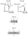
- Fig. 8 shows a plan view of a conventional surface acoustic wave resonator provided with normal type electrodes.
- normal type electrode 3 having comb electrodes 1 and reflectors 2 as shown in Fig. 8
- spurious responses attributed to the resonance in the transverse mode e.g. 9A and Fig. 9B represent a characteristic of a typical case stated above. That is, Fig. 9A shows a pass-band characteristic, which plots insertion loss versus frequency of the surface acoustic wave resonator of Fig. 8
- Fig. 9B shows a part of the pass-band characteristic of the surface acoustic wave resonator, wherein domain 9b encircled by a dotted line in Fig. 9A is enlarged.
- Fig. 10 shows a plan view of a conventional surface acoustic wave resonator of different type from that of Fig. 8 .
- This surface acoustic wave resonator is formed into a so-called apodized configuration, in which overlapping lengths of interdigitated electrode fingers of two comb electrodes 1 are varied as shown in Fig. 10 to obtain a desired frequency characteristic.
- Patent references 1 and 2 are examples of the prior art documents known to be related to the above technique.
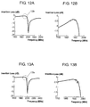
- the apodization is effective to suppress the resonance in the transverse mode of comb electrodes 1 having a small number of electrode fingers as shown in Fig. 10 , it is not feasible to suppress spurious responses if comb electrodes 1 have a large number of electrode fingers as is the case of another conventional surface acoustic wave resonator shown in Fig. 11 since it bears a high amplitude of excitation in the transverse mode.
- Fig. 12A shows a pass-band characteristic of a surface acoustic wave resonator provided with comb electrodes having 150 apodized electrode fingers
- Fig. 12B shows a part of the pass-band characteristic of the surface acoustic wave resonator, wherein domain 12b encircled by a dotted line in Fig. 12A is enlarged.
- Fig. 13A shows a pass-band characteristic of another surface acoustic wave resonator provided with comb electrodes having 300 apodized electrode fingers
- Fig. 13B shows a part of the pass-band characteristic of the surface acoustic wave resonator, wherein domain 13b encircled by a dotted line in Fig. 13A is enlarged.
- the surface acoustic wave resonator featuring the pass-band characteristic shown in Fig. 13A and Fig. 13B has such a structure that comb electrodes are formed on a LiNbO 3 substrate, and surfaces of the comb electrodes and the LiNbO 3 substrate are covered with a thin film of silicon dioxide (hereinafter referred to as "SiO 2 ").
- the substrate used here is a rotated Y-cut substrate having a cut angle of 5 degrees.
- Patent Document 1 Japanese Patent Unexamined Publication, No. 1990-11012
- Patent Document 2 Japanese Patent Unexamined Publication, No. 1994-85602
- Document JP 05 129 872 A discloses a surface wave resonator, surface wave filter, branching filter and mobile radio equipment.
- the present invention is intended to solve the above problem, and to provide a surface acoustic wave resonator featuring a wide frequency band with spurious responses suppressed even when a capacitance is increased by providing comb electrodes with a large number of electrode fingers.
- the invention comprises a surface wave resonator according to claim 1.
- the surface acoustic wave resonator of the present invention includes a piezoelectric substrate, a first surface acoustic wave resonator having a comb electrode provided on the piezoelectric substrate, and a second surface acoustic wave resonator having a comb electrode also provided on the piezoelectric substrate. Both of the first surface acoustic wave resonator and the second surface acoustic wave resonator have an apodized configuration, and they are connected in parallel.
- the above structure uses two surface acoustic wave resonators, each having a smaller number of comb electrode fingers, it can suppress undesired resonance in the transverse mode to thereby prevent spurious responses.
- the structure can also provide a desired value of electrostatic capacitance since it makes use of the first surface acoustic wave resonator and the second surface acoustic wave resonator in parallel connection.
- the present invention can provide the surface acoustic wave resonator having the desired value of electrostatic capacitance while preventing the spurious responses even with a large number of the comb electrode fingers in the aggregate.
- Fig. 1 shows a plan view of a surface acoustic wave resonator according to the first example.
- the surface acoustic wave resonator of the first example includes piezoelectric substrate 10, first surface acoustic wave resonator 20 having comb electrodes 11 provided on piezoelectric substrate 10, and second surface acoustic wave resonator 30 having comb electrodes 12 provided on piezoelectric substrate 10.
- First surface acoustic wave resonator 20 and second surface acoustic wave resonator 30 have an apodized configuration as shown in Fig. 1 , and they are connected in parallel.
- the surface acoustic wave resonator shown in the first example is comprised of comb electrodes 11 and 12, and He reflectors 13, 14, 15 and 16, all formed on piezoelectric substrate 10 made of a material such as LiNbO 3 .
- Reflectors 13 and 14 are disposed in close proximity to both sides of comb electrodes 11 to compose first surface acoustic wave resonator 20 as shown in Fig. 1 .
- reflectors 15 and 16 are disposed in close proximity to both sides of comb electrodes 12 to compose second surface acoustic wave resonator 30.
- the surface acoustic wave resonator shown in the first example is so configured that first surface acoustic wave resonator 20 and second surface acoustic wave resonator 30 are connected in parallel.
- Both comb electrodes 11 and 12 are apodized into such a configuration that overlapping lengths of their interdigitated electrode fingers are gradually reduced from the largest at the center toward both ends of the resonators where the electrode fingers are not overlapped.
- the term apodization refers to a technique in designing the surface acoustic wave resonator to obtain a desired frequency characteristic by varying overlapping lengths of the electrode fingers.
- the above structure adopted in the surface acoustic wave resonator can achieve a wideband characteristic with low spurious responses.
- Fig. 2A shows a pass-band characteristic of the surface acoustic wave resonator produced as discussed above
- Fig. 2B shows a part of the pass-band characteristic, wherein domain 2b encircled by a dotted line in Fig. 2A is enlarged.
- piezoelectric substrate 10 used here is a rotated Y-cut substrate having a cut angle of 5 degrees, and comb electrodes 11 and 12 are formed on this LiNbO 3 substrate covered with a film of silicon oxide such as SiO 2 . In other words, a dielectric layer made of the silicon oxide film is formed over the comb electrodes.
- This structure helps widen the frequency bandwidth and improve the temperature characteristic of the resonator.
- the piezoelectric substrate used here is a rotated Y-cut substrate of 5-degree cut angle
- the surface acoustic wave resonator can be produced by using a rotated Y-cut substrate of LiNbO 3 having any cut angle within a range of -5 to +30 degrees.
- the piezoelectric substrate of a high electromechanical coupling coefficient can be thus obtained by processing the rotated Y-cut of a cut angle within the range specified above, thereby making the surface acoustic wave resonator adaptable for a wideband filter. It is especially desirable to use the piezoelectric substrate, of which the rotated Y-cut angle is inside the range of -5 and +30 degrees, since this can provide the piezoelectric substrate with a high electromechanical coupling coefficient.
- Comb electrodes 11 and 12 are provided with 150 each of electrode fingers so as to make the surface acoustic wave resonator in a complete device become equivalent in value of the electrostatic capacitance to that of the conventional surface acoustic wave resonator having 300 fingers of the comb electrodes shown in Fig. 11 .
- first surface acoustic wave resonator 20 and second surface acoustic wave resonator 30 having comb electrodes 11 and 12 each provided with the smaller number of the electrode fingers, which work effectively to suppress the undesired resonances in the transverse mode. It is also because of the large electrostatic capacitance of the complete surface acoustic wave resonator obtained by the parallel connection between first surface acoustic wave resonator 20 and second surface acoustic wave resonator 30.
- Adoption of the above structure can hence realize the surface acoustic wave resonator of large capacitance while also suppressing the spurious responses. Accordingly, it can be anticipated that the structure provides an advantage effect of increasing a degree of flexibility in designing ladder type filters.
- Fig. 3 shows a plan view of a surface acoustic wave resonator according to the first exemplary embodiment.
- This surface acoustic wave resonator includes first surface acoustic wave resonator 21 and second surface acoustic wave resonator 22, which are connected in parallel in the same fashion as Fig. 1 .
- First surface acoustic wave resonator 21 includes comb electrodes 21a and reflectors 21b and 21c disposed in a manner to sandwich comb electrodes 21a.
- Second surface acoustic wave resonator 22 includes comb electrodes 22a and reflectors 22b and 22c also disposed in a manner to sandwich comb electrodes 22a.
- first surface acoustic wave resonator 21 and second surface acoustic wave resonator 22 are formed different in their overlapping lengths L1 and L2 such that they have a relation of L1 > L2, as shown in Fig. 3 , to obtain the following advantage.
- Spurious response to resonance in the transverse mode discussed here referred to the spurious response that occurs within the passing frequency band due to standing waves developed in a direction orthogonal to the propagating direction X of elastic waves.
- a frequency of the spurious response in the transverse mode is therefore dependent upon the overlapping lengths L1 and L2 of comb electrodes 21a and 22a of first surface acoustic wave resonator 21 and second surface acoustic wave resonator 22.
- the overlapping lengths L1 and L2 are set to have the relation of L1 > L2 to differentiate the resonance frequencies in the transverse mode between first surface acoustic wave resonator 21 and second surface acoustic wave resonator 22, so as to separate the spurious responses to the transverse mode resonances.
- This helps suppress a magnitude of the spurious responses in a specific frequency band. It becomes possible to realize the surface acoustic wave resonator featuring a superior resonance characteristic while also achieving further reduction of the insertion loss by virtue of using this method of differentiating the overlapping lengths for suppression of the spurious responses in combination with the design of apodization for suppressing the spurious responses to the transverse mode resonances.
- Fig. 4 shows a plan view of a surface acoustic wave resonator according to the second example.
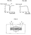
- the surface acoustic wave resonator has a structure, in which either reflector 14 or reflector 15 between comb electrodes 11 and 12 shown in Fig. 1 is eliminated, so that the remaining element designated as reflector 15 is used to serve commonly for both comb electrodes 11 and 12.
- first surface acoustic wave resonator 21 and second surface acoustic wave resonator 22 share a function of reflector 15 provided between them.
- This structure allows further reduction in size of the surface acoustic wave resonator as compared to the one shown in Fig. 1 of the first example embodiment.
- Fig. 5A shows a pass-band characteristic of this surface acoustic wave resonator
- Fig. 5B shows a part of the pass-band characteristic, wherein domain 5b encircled by a dotted line in Fig. 5A is enlarged.
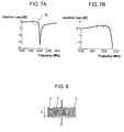
- Fig. 6 shows a plan view of a surface acoustic wave resonator according to the third example.
- the surface acoustic wave resonator has a structure, in which both reflectors 14 and 15 located between comb electrodes 11 and 12 shown in Fig. 1 are eliminated, and comb electrodes 11 and 12 are disposed close to each other.
- first surface acoustic wave resonator 21 and second surface acoustic wave resonator 22 share functions of reflectors 13 and 16 that sandwich comb electrodes 11 and 12 between them.
- This structure allows even further reduction in size of the surface acoustic wave resonator as compared to those discussed in the first and the second examples.
- Fig. 7A shows a pass-band characteristic of this surface acoustic wave resonator
- Fig. 7B shows a part of the pass-band characteristic, wherein domain 7b encircled by a dotted line in Fig. 7A is enlarged.
- first surface acoustic wave resonator 21 and second surface acoustic wave resonator 22 are apodized by respective weights and connected in parallel.
- the comb electrodes are apodized in the configuration that overlapping lengths of the interdigitated electrode fingers are gradually reduced from the largest at the center toward both ends of the resonators where the electrode fingers are not overlapped, but this configuration is just illustrative and not restrictive.
- the structure can be optimized to obtain the most suitable surface acoustic wave resonator by varying levels of the weights with consideration given to a magnitude of the spurious responses in the transverse mode.
- first through the third examples show the structures comprising first surface acoustic wave resonator 21 and second surface acoustic wave resonator 22 connected in parallel, this invention is also applicable to a structure having three or more resonators in parallel connection rather than just two.
- numbers of the electrode fingers and their configurations as well as weights placed on comb electrodes 11 and 12 may be designed differently between first surface acoustic wave resonator 21 and second surface acoustic wave resonator 22 though the above examples have shown them as being identical in their configurations.
- the surface acoustic wave resonator provided by this invention features superior suppression of spurious responses even with a large number of the comb electrode fingers in the aggregate, has a predetermined value of electrostatic capacitance and a low insertion loss while also achieving a reduction in size.
- This resonator is therefore suitable as an electronic component for use in any kind of electronic apparatus, and contributable to improvement of the performance and downsizing of the electronic apparatus.
Landscapes
- Physics & Mathematics (AREA)
- Acoustics & Sound (AREA)
- Chemical & Material Sciences (AREA)
- Engineering & Computer Science (AREA)
- Materials Engineering (AREA)
- Surface Acoustic Wave Elements And Circuit Networks Thereof (AREA)
Claims (5)
- Résonateur à ondes acoustiques de surface comprenant :- un substrat piézoélectrique (10) ;- un premier résonateur à ondes acoustiques de surface (22) ayant une électrode en peigne (22a) situé sur le substrat piézoélectrique (10) ; et- un second résonateur à ondes acoustiques de surface (21) ayant une électrode en peigne (21a) situé sur le substrat piézoélectrique (10),
dans lequel une réponse parasite se produit dans la bande de fréquences de passage en raison d'ondes stationnaires développées dans une direction orthogonale à la direction de propagation,
dans lequel une fréquence de la réponse parasite dans le mode transversal dépend des longueurs de chevauchement L1 et L2 des électrodes en peigne (22a, 21a) du premier résonateur à ondes acoustiques de surface (22) et du second résonateur à ondes acoustiques de surface (21),
dans lequel le premier résonateur à ondes acoustiques de surface (22) et le second résonateur à ondes acoustiques de surface (21) sont apodisés, dans lequel par le terme apodisation on entend une technique dans la conception du résonateur à ondes acoustiques de surface pour obtenir une caractéristique de fréquence souhaitée en faisant varier les longueurs de chevauchement des doigts d'électrodes, et dans lequel le premier résonateur à ondes acoustiques de surface (22) et le second résonateur à ondes acoustiques de surface (21) sont connectés en parallèle,
dans lequel les électrodes en peigne du premier résonateur à ondes acoustiques de surface et du second résonateur à ondes acoustiques de surface (21a, 22a) sont formées avec des longueurs de chevauchement différentes L1 et L2, de telle sorte qu'elles ont une relation L1 > L2 pour différencier les fréquences de résonance dans le mode transversal entre le premier résonateur à ondes acoustiques de surface (22) et le second résonateur à ondes acoustiques de surface (21) de manière à séparer les réponses parasites pour les résonances en mode transversal. - Résonateur à ondes acoustiques de surface selon la revendication 1, dans lequel le substrat piézoélectrique (10) est formé d'un LiNbO3.
- Résonateur à ondes acoustiques de surface selon la revendication 1, dans lequel le substrat piézoélectrique (10) est formé d'un substrat de LiNbO3 coupe Y pivotée ayant un angle de coupe compris dans la plage de -5 à 30 degrés, et une couche diélectrique est formée sur les électrodes en peigne (21a, 22a).
- Résonateur à ondes acoustiques de surface selon la revendication 1, dans lequel le premier résonateur à ondes acoustiques de surface et le second résonateur à ondes acoustiques de surface (21, 22) partagent au moins un réflecteur.
- Résonateur à ondes acoustiques de surface selon la revendication 1, dans lequel au moins l'une des électrodes en peigne (21a, 22a) du premier résonateur à ondes acoustiques de surface et du second résonateur à ondes acoustiques de surface (21, 22) comporte 150, ou moins, en nombre de doigts d'électrode.
Priority Applications (1)
| Application Number | Priority Date | Filing Date | Title |
|---|---|---|---|
| EP15177694.5A EP2963818B1 (fr) | 2006-11-08 | 2007-11-07 | Résonateur à ondes acoustiques de surface |
Applications Claiming Priority (2)
| Application Number | Priority Date | Filing Date | Title |
|---|---|---|---|
| JP2006302346 | 2006-11-08 | ||
| PCT/JP2007/071626 WO2008056697A1 (fr) | 2006-11-08 | 2007-11-07 | Résonateur d'onde acoustique de surface |
Related Child Applications (1)
| Application Number | Title | Priority Date | Filing Date |
|---|---|---|---|
| EP15177694.5A Division EP2963818B1 (fr) | 2006-11-08 | 2007-11-07 | Résonateur à ondes acoustiques de surface |
Publications (3)
| Publication Number | Publication Date |
|---|---|
| EP2091146A1 EP2091146A1 (fr) | 2009-08-19 |
| EP2091146A4 EP2091146A4 (fr) | 2009-12-09 |
| EP2091146B1 true EP2091146B1 (fr) | 2015-07-22 |
Family
ID=39364511
Family Applications (2)
| Application Number | Title | Priority Date | Filing Date |
|---|---|---|---|
| EP07831357.4A Withdrawn - After Issue EP2091146B1 (fr) | 2006-11-08 | 2007-11-07 | Résonateur d'onde acoustique de surface |
| EP15177694.5A Active EP2963818B1 (fr) | 2006-11-08 | 2007-11-07 | Résonateur à ondes acoustiques de surface |
Family Applications After (1)
| Application Number | Title | Priority Date | Filing Date |
|---|---|---|---|
| EP15177694.5A Active EP2963818B1 (fr) | 2006-11-08 | 2007-11-07 | Résonateur à ondes acoustiques de surface |
Country Status (4)
| Country | Link |
|---|---|
| US (1) | US8084915B2 (fr) |
| EP (2) | EP2091146B1 (fr) |
| JP (3) | JP4706756B2 (fr) |
| WO (1) | WO2008056697A1 (fr) |
Cited By (1)
| Publication number | Priority date | Publication date | Assignee | Title |
|---|---|---|---|---|
| FR3105894A1 (fr) | 2019-12-30 | 2021-07-02 | Frec'n'sys | Structure de transducteur pour résonateur à accès unique |
Families Citing this family (9)
| Publication number | Priority date | Publication date | Assignee | Title |
|---|---|---|---|---|
| JP5273247B2 (ja) * | 2009-05-29 | 2013-08-28 | 株式会社村田製作所 | ラダー型フィルタ |
| RU2491712C1 (ru) * | 2012-01-10 | 2013-08-27 | Федеральное государственное унитарное предприятие "Ростовский-на-Дону научно-исследовательский институт радиосвязи" (ФГУП "РНИИРС") | Резонатор на поверхностных акустических волнах с использованием отражателей в качестве нагревательных элементов |
| US9093979B2 (en) | 2012-06-05 | 2015-07-28 | Avago Technologies General Ip (Singapore) Pte. Ltd. | Laterally-coupled acoustic resonators |
| JP6186220B2 (ja) | 2013-09-12 | 2017-08-23 | 日本電波工業株式会社 | 弾性波フィルタ |
| SG11201903365SA (en) * | 2016-10-20 | 2019-05-30 | Skyworks Solutions Inc | Elastic wave device with sub-wavelength thick piezoelectric layer |
| WO2018117060A1 (fr) * | 2016-12-19 | 2018-06-28 | 株式会社村田製作所 | Résonateur à ondes acoustiques, dispositif de filtre et multiplexeur |
| DE102019121866A1 (de) * | 2019-08-14 | 2021-02-18 | RF360 Europe GmbH | SAW-Resonator-Kaskade |
| US12506464B2 (en) | 2021-12-06 | 2025-12-23 | Skyworks Solutions, Inc. | Multi-band surface acoustic wave filters |
| US12525494B2 (en) | 2022-03-30 | 2026-01-13 | Skyworks Solutions, Inc. | Composited carrier for microphone package |
Family Cites Families (29)
| Publication number | Priority date | Publication date | Assignee | Title |
|---|---|---|---|---|
| GB1355418A (en) * | 1971-05-24 | 1974-06-05 | Mullard Ltd | Acoustic surface wave devices |
| DE3267639D1 (en) * | 1981-02-04 | 1986-01-09 | Matsushita Electric Industrial Co Ltd | Surface acoustic wave device |
| JPS60154706A (ja) * | 1984-01-25 | 1985-08-14 | Toshiba Corp | 弾性表面波フイルタ装置 |
| JPS63260213A (ja) * | 1986-09-12 | 1988-10-27 | Hiroshi Shimizu | 高結合ラブ波型saw基板を用いた共振子 |
| JPH0211012A (ja) | 1988-06-29 | 1990-01-16 | Toko Inc | 表面弾性波多重モードフィルタ |
| GB2259818B (en) * | 1991-09-17 | 1995-08-16 | Racal Mesl Ltd | Surface acoustic wave (saw) ladder transducer |
| JPH0685493B2 (ja) | 1991-10-14 | 1994-10-26 | 国際電気株式会社 | 弾性表面波共振子 |
| JPH05129872A (ja) | 1991-11-07 | 1993-05-25 | Hitachi Ltd | 表面波共振子、表面波フイルタ、分波器および移動無線装置 |
| JPH0786871A (ja) * | 1993-09-09 | 1995-03-31 | Sanyo Electric Co Ltd | 弾性表面波高周波フィルタ |
| DE4431612C2 (de) * | 1993-09-06 | 1998-07-16 | Sanyo Electric Co | Akustisches Oberflächenwellenfilter |
| JPH07162261A (ja) * | 1993-12-09 | 1995-06-23 | Sanyo Electric Co Ltd | 多重電極型弾性表面波フィルタ |
| JPH08321740A (ja) * | 1995-05-24 | 1996-12-03 | Nec Corp | 弾性表面波デバイス |
| JPH09205341A (ja) * | 1996-01-29 | 1997-08-05 | Kinseki Ltd | 弾性表面波フイルタ |
| JPH10261936A (ja) * | 1997-03-19 | 1998-09-29 | Mitsubishi Electric Corp | 弾性表面波フィルタ |
| JPH1174751A (ja) | 1997-08-28 | 1999-03-16 | Murata Mfg Co Ltd | 弾性表面波装置 |
| JPH1188100A (ja) | 1997-09-03 | 1999-03-30 | Toyo Commun Equip Co Ltd | 弾性表面波デバイス |
| JP2000286675A (ja) * | 1999-03-29 | 2000-10-13 | Sanyo Electric Co Ltd | 弾性表面波フィルター装置及びこれを具えた携帯電話機 |
| JP3449352B2 (ja) * | 2000-02-07 | 2003-09-22 | 株式会社村田製作所 | 弾性表面波フィルタ |
| JP4109877B2 (ja) * | 2001-03-04 | 2008-07-02 | 和彦 山之内 | 弾性表面波機能素子 |
| EP1239588A2 (fr) | 2001-03-04 | 2002-09-11 | Kazuhiko Yamanouchi | Substrat pour ondes acoustiques de surface et élément fonctionnel à ondes acoustiques de surface |
| JP3534080B2 (ja) * | 2001-03-23 | 2004-06-07 | 株式会社村田製作所 | 弾性表面波フィルタ装置 |
| JP3764731B2 (ja) * | 2002-10-18 | 2006-04-12 | 富士通メディアデバイス株式会社 | 多重モード弾性表面波フィルタ及び分波器 |
| DE112004001841B4 (de) * | 2003-10-03 | 2009-03-12 | Murata Mfg. Co., Ltd., Nagaokakyo-shi | Oberflächenwellenbauelement |
| JP4668178B2 (ja) * | 2004-04-28 | 2011-04-13 | パナソニック株式会社 | 弾性表面波共振子 |
| US7579928B2 (en) * | 2006-04-03 | 2009-08-25 | Kyocera Corporation | Surface acoustic wave device and communication device |
| KR100954292B1 (ko) * | 2006-09-22 | 2010-04-26 | 가부시키가이샤 무라타 세이사쿠쇼 | 종결합 공진자형 탄성파 필터장치 |
| CN101517894B (zh) * | 2006-09-28 | 2011-12-28 | 株式会社村田制作所 | 弹性波滤波装置 |
| JP2008131128A (ja) * | 2006-11-17 | 2008-06-05 | Matsushita Electric Ind Co Ltd | 弾性表面波フィルタ、アンテナ共用器、およびそれらの製造方法 |
| US7569971B2 (en) * | 2007-10-02 | 2009-08-04 | Delaware Capital Formation, Inc. | Compensation of resonators for substrate and transducer asymmetry |
-
2007
- 2007-11-07 EP EP07831357.4A patent/EP2091146B1/fr not_active Withdrawn - After Issue
- 2007-11-07 WO PCT/JP2007/071626 patent/WO2008056697A1/fr not_active Ceased
- 2007-11-07 EP EP15177694.5A patent/EP2963818B1/fr active Active
- 2007-11-07 JP JP2008543100A patent/JP4706756B2/ja active Active
- 2007-11-07 US US12/513,903 patent/US8084915B2/en active Active
-
2011
- 2011-03-03 JP JP2011046211A patent/JP4784707B2/ja active Active
- 2011-05-24 JP JP2011115485A patent/JP4788846B2/ja active Active
Cited By (4)
| Publication number | Priority date | Publication date | Assignee | Title |
|---|---|---|---|---|
| FR3105894A1 (fr) | 2019-12-30 | 2021-07-02 | Frec'n'sys | Structure de transducteur pour résonateur à accès unique |
| WO2021136756A1 (fr) | 2019-12-30 | 2021-07-08 | Frec'n'sys | Structure de transducteur pour résonateur à port unique avec suppression de mode transversal |
| DE112020006401T5 (de) | 2019-12-30 | 2022-10-13 | Frec'n'sys | Wandlerstruktur für einen Eintor-Resonator |
| US12542532B2 (en) | 2019-12-30 | 2026-02-03 | Soitec | Transducer structure for single-port resonator |
Also Published As
| Publication number | Publication date |
|---|---|
| EP2963818B1 (fr) | 2023-06-28 |
| US8084915B2 (en) | 2011-12-27 |
| JPWO2008056697A1 (ja) | 2010-02-25 |
| US20100060103A1 (en) | 2010-03-11 |
| JP2011160488A (ja) | 2011-08-18 |
| JP4706756B2 (ja) | 2011-06-22 |
| EP2091146A1 (fr) | 2009-08-19 |
| JP4784707B2 (ja) | 2011-10-05 |
| JP2011139513A (ja) | 2011-07-14 |
| JP4788846B2 (ja) | 2011-10-05 |
| EP2963818A1 (fr) | 2016-01-06 |
| WO2008056697A1 (fr) | 2008-05-15 |
| EP2091146A4 (fr) | 2009-12-09 |
Similar Documents
| Publication | Publication Date | Title |
|---|---|---|
| EP2091146B1 (fr) | Résonateur d'onde acoustique de surface | |
| KR102166218B1 (ko) | 필터 | |
| US7688161B2 (en) | Acoustic wave device and filter using the same | |
| JP5569621B2 (ja) | アンテナ共用器およびラダー型フィルタとそれを搭載した電子機器 | |
| WO2019117133A1 (fr) | Multiplexeur, circuit frontal haute fréquence, et dispositif de communication | |
| EP2068444B1 (fr) | Filtre d'onde acoustique | |
| WO2018168836A1 (fr) | Élément à ondes acoustiques, dispositif de filtre à ondes acoustiques et multiplexeur | |
| JP6801797B2 (ja) | 弾性波フィルタ | |
| US10958241B2 (en) | Extractor | |
| JP5158725B2 (ja) | 弾性表面波装置およびそれを用いた通信装置 | |
| WO2010131450A1 (fr) | Dispositif de partage d'antenne | |
| WO2020137263A1 (fr) | Dispositif de filtrage | |
| KR101044971B1 (ko) | 탄성 표면파 필터 | |
| US8525621B2 (en) | Boundary acoustic wave filter | |
| JP7103420B2 (ja) | フィルタ装置およびマルチプレクサ | |
| JP3745847B2 (ja) | 二重モードsawフィルタの構造 | |
| CN221553235U (zh) | 弹性波元件、弹性波滤波器装置及多工器 | |
| CN118399925A (zh) | 多工器 | |
| WO2023090238A1 (fr) | Multiplexeur |
Legal Events
| Date | Code | Title | Description |
|---|---|---|---|
| PUAI | Public reference made under article 153(3) epc to a published international application that has entered the european phase |
Free format text: ORIGINAL CODE: 0009012 |
|
| 17P | Request for examination filed |
Effective date: 20090422 |
|
| AK | Designated contracting states |
Kind code of ref document: A1 Designated state(s): AT BE BG CH CY CZ DE DK EE ES FI FR GB GR HU IE IS IT LI LT LU LV MC MT NL PL PT RO SE SI SK TR |
|
| A4 | Supplementary search report drawn up and despatched |
Effective date: 20091105 |
|
| RIC1 | Information provided on ipc code assigned before grant |
Ipc: H03H 9/02 20060101ALI20091030BHEP Ipc: H03H 9/25 20060101ALI20091030BHEP Ipc: H03H 9/145 20060101AFI20080529BHEP |
|
| 17Q | First examination report despatched |
Effective date: 20100104 |
|
| DAX | Request for extension of the european patent (deleted) | ||
| REG | Reference to a national code |
Ref country code: DE Ref legal event code: R079 Ref document number: 602007042283 Country of ref document: DE Free format text: PREVIOUS MAIN CLASS: H03H0009145000 Ipc: H03H0009020000 |
|
| GRAP | Despatch of communication of intention to grant a patent |
Free format text: ORIGINAL CODE: EPIDOSNIGR1 |
|
| RIC1 | Information provided on ipc code assigned before grant |
Ipc: H03H 9/145 20060101ALI20150126BHEP Ipc: H03H 9/02 20060101AFI20150126BHEP Ipc: H03H 9/25 20060101ALI20150126BHEP |
|
| INTG | Intention to grant announced |
Effective date: 20150212 |
|
| GRAS | Grant fee paid |
Free format text: ORIGINAL CODE: EPIDOSNIGR3 |
|
| GRAA | (expected) grant |
Free format text: ORIGINAL CODE: 0009210 |
|
| AK | Designated contracting states |
Kind code of ref document: B1 Designated state(s): AT BE BG CH CY CZ DE DK EE ES FI FR GB GR HU IE IS IT LI LT LU LV MC MT NL PL PT RO SE SI SK TR |
|
| RAP1 | Party data changed (applicant data changed or rights of an application transferred) |
Owner name: SKYWORKS PANASONIC FILTER SOLUTIONS JAPAN CO., LTD |
|
| REG | Reference to a national code |
Ref country code: GB Ref legal event code: FG4D |
|
| PUAC | Information related to the publication of a b1 document modified or deleted |
Free format text: ORIGINAL CODE: 0009299EPPU |
|
| REG | Reference to a national code |
Ref country code: CH Ref legal event code: PK Free format text: DIE ERTEILUNG WURDE VOM EPA WIDERRUFEN. Ref country code: CH Ref legal event code: EP |
|
| STAA | Information on the status of an ep patent application or granted ep patent |
Free format text: STATUS: THE APPLICATION HAS BEEN WITHDRAWN |
|
| REG | Reference to a national code |
Ref country code: IE Ref legal event code: FG4D |
|
| REG | Reference to a national code |
Ref country code: AT Ref legal event code: REF Ref document number: 738387 Country of ref document: AT Kind code of ref document: T Effective date: 20150815 |
|
| DB1 | Publication of patent cancelled |
Effective date: 20150724 |
|
| 18W | Application withdrawn |
Effective date: 20150721 |
|
| REG | Reference to a national code |
Ref country code: NL Ref legal event code: GRER Effective date: 20150826 |
|
| REG | Reference to a national code |
Ref country code: DE Ref legal event code: R096 Ref document number: 602007042283 Country of ref document: DE |
|
| REG | Reference to a national code |
Ref country code: DE Ref legal event code: R107 Ref document number: 602007042283 Country of ref document: DE |
|
| REG | Reference to a national code |
Ref country code: CH Ref legal event code: PK Free format text: DAS LOESCHDATUM WURDE ERGAENZT / LE CHAMP DATE DE RADIATION A ETE COMPLETE / LA DATA DI CANCELLAZIONE E STATA COMPLETATA |