EP2093798A2 - Marche rétractable pour véhicules à moteur - Google Patents
Marche rétractable pour véhicules à moteur Download PDFInfo
- Publication number
- EP2093798A2 EP2093798A2 EP09151145A EP09151145A EP2093798A2 EP 2093798 A2 EP2093798 A2 EP 2093798A2 EP 09151145 A EP09151145 A EP 09151145A EP 09151145 A EP09151145 A EP 09151145A EP 2093798 A2 EP2093798 A2 EP 2093798A2
- Authority
- EP
- European Patent Office
- Prior art keywords
- chip
- substrate
- ipd
- array
- interconnection
- Prior art date
- Legal status (The legal status is an assumption and is not a legal conclusion. Google has not performed a legal analysis and makes no representation as to the accuracy of the status listed.)
- Withdrawn
Links
Images


Classifications
-
- H—ELECTRICITY
- H10—SEMICONDUCTOR DEVICES; ELECTRIC SOLID-STATE DEVICES NOT OTHERWISE PROVIDED FOR
- H10W—GENERIC PACKAGES, INTERCONNECTIONS, CONNECTORS OR OTHER CONSTRUCTIONAL DETAILS OF DEVICES COVERED BY CLASS H10
- H10W40/00—Arrangements for thermal protection or thermal control
- H10W40/10—Arrangements for heating
-
- H—ELECTRICITY
- H10—SEMICONDUCTOR DEVICES; ELECTRIC SOLID-STATE DEVICES NOT OTHERWISE PROVIDED FOR
- H10W—GENERIC PACKAGES, INTERCONNECTIONS, CONNECTORS OR OTHER CONSTRUCTIONAL DETAILS OF DEVICES COVERED BY CLASS H10
- H10W90/00—Package configurations
-
- H—ELECTRICITY
- H10—SEMICONDUCTOR DEVICES; ELECTRIC SOLID-STATE DEVICES NOT OTHERWISE PROVIDED FOR
- H10W—GENERIC PACKAGES, INTERCONNECTIONS, CONNECTORS OR OTHER CONSTRUCTIONAL DETAILS OF DEVICES COVERED BY CLASS H10
- H10W70/00—Package substrates; Interposers; Redistribution layers [RDL]
- H10W70/60—Insulating or insulated package substrates; Interposers; Redistribution layers
-
- H—ELECTRICITY
- H10—SEMICONDUCTOR DEVICES; ELECTRIC SOLID-STATE DEVICES NOT OTHERWISE PROVIDED FOR
- H10W—GENERIC PACKAGES, INTERCONNECTIONS, CONNECTORS OR OTHER CONSTRUCTIONAL DETAILS OF DEVICES COVERED BY CLASS H10
- H10W44/00—Electrical arrangements for controlling or matching impedance
- H10W44/20—Electrical arrangements for controlling or matching impedance at high-frequency [HF] or radio frequency [RF]
-
- H—ELECTRICITY
- H10—SEMICONDUCTOR DEVICES; ELECTRIC SOLID-STATE DEVICES NOT OTHERWISE PROVIDED FOR
- H10W—GENERIC PACKAGES, INTERCONNECTIONS, CONNECTORS OR OTHER CONSTRUCTIONAL DETAILS OF DEVICES COVERED BY CLASS H10
- H10W44/00—Electrical arrangements for controlling or matching impedance
- H10W44/20—Electrical arrangements for controlling or matching impedance at high-frequency [HF] or radio frequency [RF]
- H10W44/241—Electrical arrangements for controlling or matching impedance at high-frequency [HF] or radio frequency [RF] for passive devices or passive elements
-
- H—ELECTRICITY
- H10—SEMICONDUCTOR DEVICES; ELECTRIC SOLID-STATE DEVICES NOT OTHERWISE PROVIDED FOR
- H10W—GENERIC PACKAGES, INTERCONNECTIONS, CONNECTORS OR OTHER CONSTRUCTIONAL DETAILS OF DEVICES COVERED BY CLASS H10
- H10W72/00—Interconnections or connectors in packages
- H10W72/851—Dispositions of multiple connectors or interconnections
- H10W72/874—On different surfaces
- H10W72/877—Bump connectors and die-attach connectors
-
- H—ELECTRICITY
- H10—SEMICONDUCTOR DEVICES; ELECTRIC SOLID-STATE DEVICES NOT OTHERWISE PROVIDED FOR
- H10W—GENERIC PACKAGES, INTERCONNECTIONS, CONNECTORS OR OTHER CONSTRUCTIONAL DETAILS OF DEVICES COVERED BY CLASS H10
- H10W90/00—Package configurations
- H10W90/701—Package configurations characterised by the relative positions of pads or connectors relative to package parts
- H10W90/721—Package configurations characterised by the relative positions of pads or connectors relative to package parts of bump connectors
- H10W90/724—Package configurations characterised by the relative positions of pads or connectors relative to package parts of bump connectors between a chip and a stacked insulating package substrate, interposer or RDL
Definitions
- This invention relates to multi-chip module (MCM) integrated circuit packages and more specifically to Integrated Passive Device (IPD) packages with improved thermal control.
- MCM multi-chip module
- IPD Integrated Passive Device
- IPD packaging in general presents a special case. Size reductions in IPD/RF packaging technology have lagged a step behind IC MCM packaging. This is partly due to the inherently larger size of IPD substrates. IPD packaging is also influenced by the presence of analog components in the RF and IPD subassemblies, and the need to account for stray electromagnetic effects. Thus stacking IPDs with other circuit elements as commonly done in transistor IC MCM packages has been constrained.
- MCM integrated circuit packages containing RF chips are described, for example, in United States Patent No. 5,869,894 .
- the MCM configuration described there demonstrates one aspect of the limitations on thickness of MCM packages.
- the RF chip is located in the stand-off between a relatively larger IC host chip, for example a memory of logic chip, and a substrate.
- the RF chip is bonded to the host chip, and the pair is flip-chip bonded to the substrate.
- This arrangement allows the ground plane of the RF chip to be conveniently interconnected directly to a ground plane on the substrate.
- an intermediate interconnect substrate is used.
- An improved RF/IPD package has been developed with significantly reduced thickness, and with improved thermal management.
- An embodiment of improved package is described in general as follows.
- the IPD substrate is attached to a system substrate.
- a very thin RF chip is mounted in the standoff between the IPD substrate and the system substrate, RF interconnections are made between the top of the RF chip and the bottom of the IPD substrate.
- the very thin RF chip requires unconventional means for heat dissipation.
- a heat sink is provided between the RF chip and the system substrate.
- the heat sink may also serve as a ground plane connection.
- the combination of a very thin RF chip specially mounted on an IPD represents a subassembly according to the invention. In the preferred embodiment the subassembly is an RF/IPD combination.
- RF/IC, IC/IPD, or IC/IC combinations may be produced according to these teachings.
- a conventional stacked MCM comprising substrate 11, with intermediate interconnect substrate (IIS) 12 bonded to the substrate with solder bumps 13.
- IIS intermediate interconnect substrate
- a first MCM IC chip 14 is mounted on top of the IIS and attached with solder bumps 15.
- a second MCM IC chip 16 is shown occupying the space between the first MCM IC chip 14 and the substrate 11.
- the space between the bottom of the IC chip and the substrate 11 is referred to as the standoff space and has height s in the figure.
- the height of the standoff space is important. Sufficient height is required to accommodate an IC chip in the space.
- the standoff space is created by the IIS 12.
- Typical stacked MCM packages where an IC component is mounted in a standoff space will have one or more IIS elements to create the standoff.
- the standoff space is reduced. This makes even more essential the role of one or more IIS elements to provide adequate standoff for packages that utilize the standoff space for mounting additional IC elements.
- Fig. 2 shows an RF/IPD package according to a preferred embodiment of the invention.
- the preferred embodiment comprises an RF/IPD combination, and that combination will be used as an example of the broader categories of IPD/IC and IC/IC.
- the term "integrated device" is used to encompass both IC devices and IPD devices.
- the IPD device 24 is shown attached directly to system substrate 21 with solder bumps 23.
- the IPD device substrate may be laminate, ceramic, silicon, or other appropriate material.
- the substrate 21 may be a single or multi-level interconnection substrate, for example, a single or multi-level printed wiring board. A cutaway portion of the substrate is shown in the figure to illustrate that the substrate may be a system board, and may be considerably larger than the IPD device to accommodate several IPD and IC devices.
- RF IC chip 26 is attached to the IPD device 24 with solder bumps 27. While the figures in the drawing are not to scale, it should be appreciated that the standoff space in the arrangement of Fig. 2 is small, too small to accommodate an additional chip in a conventional arrangement. This is due largely to the omission of an IIS. To fit the IC chip in the standoff space the IC chip 26 is very thin. However, it still does not fit in the standoff in the manner shown in Fig. 1 , where the standoff space S provides a gap between the RF IC chip 16 and the substrate 11. Instead of providing a gap between RF chip 26 and the substrate, the IC chip is attached to the substrate via solder attachment 28.
- the IC chip 26 is an RF power chip, for example, a power amplifier, which generates significant amounts of both electromagnetic noise and heat.
- the solder attachment 28 functions as a heat sink for RF IC chip 26. It also connects the RF chip to a ground plane on the substrate.
- the IPD substrate should be significantly larger than the RF IC chip to provide space for the direct interconnections between the IPD substrate and the system substrate.
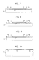
- Figs. 3-6 illustrate a fabrication sequence for a stacked RF/IPD package similar to that of Fig. 2 .
- a flip-chip assembly technique is used.
- the stacked RF chip/IPD subassembly, and the substrate, are prepared separately, then the stacked RF/IPD subassembly is flip-chip bonded to the substrate.
- Other suitable options may be used.
- Fig. 3 shows IPD device 33 with RF power chip 31 attached to the surface of the IPD device with solder attachments 32. Both of the components 31 and 33 are typically provided with bond pads and under bump metallization.
- Under bump metallization (UBM) is well known. It provides a robust, wettable, corrosion free, interface for solder interconnections. For simplicity in this description the bond pads and the UBM are not shown. However, it should be understood that the solder attachments described herein are provided with the conventional means necessary for reliable solder attachments.
- a heat sink layer 34 is applied to the backside of the RF chip as shown.
- the heat sink layer may also serve as a metallization layer for flip-chip bonding.
- the heat sink metallization should be applied directly to the semiconductor and any oxide that has been grown or deposited, or native oxide formed during processing, should be removed prior to applying the heat sink layer.
- the chip is not an RF chip, or if the heat sink metallization is not needed as a ground plane contact, other arrangements may be suitable.
- the top layer of the chip It is preferred to apply the heat sink layer to the chip at the wafer stage, where it can be applied at any convenient point in the wafer fabrication sequence.
- the material used for the heat sink layer may be any appropriate thermally conductive material, e.g. Au, Au-Sn, Cr/CrCu/Cu, TiPdAu, Al, Ag-Sn, Ag-Sn-Cu, etc.
- a superior solder wettable metal such as TiPdAu may be preferred as it facilitates direct soldering to the heat sink layer on the substrate.
- a typical thickness (height) for the IPD substrate is 100-350 microns, preferably less than 250 microns, or even less than 200 microns.
- the RF power chip 31 is typically 50-300 microns thick, preferably less than 100 microns and optimally less than 75 microns.
- IC chips with a thickness less than 100 microns can be produced using state of the art technology; in many cases IC chip thinning technology.
- Fig. 4 shows the application of solder bumps 43 to bond pads (not shown) on the substrate.
- the solder is preferably a lead free alloy, for example Au-Sn or Ag-Sn. It is chosen for both thermal conductivity and high electrical conductivity. Gold, silver, and copper alloys are preferred.
- Solder bumps 43 may be described by the generic term bonding bodies, and the size of the bonding bodies largely determines the standoff between the bottom surface of the IPD substrate and the top surface of the system substrate. As mentioned above, the bonding bodies are formed over bond pads and UBM. To increase the standoff the thickness of the bond pads and/or the UBM under the bonding bodies may be enhanced. Conductive spacers may be added for the same purpose.
- the bonding bodies may assume a variety of constructions. Solder has been mentioned above. Metal posts or columns may be used and these may be formed by any suitable method. Another alternative is shown in Figs. 5A and 5B .
- a gold wire bond is attached to the IPD surface.
- the IPD surface would normally carry a series of bond pads (not shown).
- the end of the gold wire is attached to one surface by arc welding. This results in the formation of a gold bump 46.
- the remaining gold wire is shown at 47, protruding from the gold bump 46.
- the other end is normally attached to another bond pad. However, the wire may be severed leaving the gold bump 46.
- Gold bumps that are produced in this manner may be used to attach the RF/IPD subassembly to a system board.
- the attachment method may be thermocompression bonding, or may employ gold alloy solder.
- Figs. 6-9 An especially useful step sequence is represented by Figs. 6-9 .
- the general objective of this sequence is to produce a robust subassembly of an RF chip and an IPD. That subassembly may be manufactured and sold as a unit component to system integrators.
- Fig. 6 shows the structure of Fig. 4 without the bonding bodies 43.
- the structure is coated with a polymer layer 61.
- This layer may serve as an underfill in the finished subassembly.
- the thickness of layer 61 is preferably chosen so that the surface of the heat sink layer 34 remains exposed.
- the material of layer 61 may be any suitable prepolymer material. It may be a photodefinable polymer, such as a photosensitive polyacrylate or photosensitive polyamide. It may be one of a variety of photoresists. Layer 61 may then be patterned by photodefinition to produce the structure shown in Fig. 7 . In Fig. 7 sites for bonding bodies are shown at 63.
- openings 63 may be formed by laser drilling, by photoresist and etching, or by any suitable method.
- Fig. 8 shows the openings for the bonding bodies filled with solder paste 65.
- Fig. 9 shows the bonding bodies 66 after reflow,
- Figs. 4-9 represent a preferred embodiment wherein the solder means attaching the IPD device 24 ( Fig. 2 ) to substrate 21 are formed on the IPD subassembly.
- a variety of attachment approaches may be used for this attachment.
- Solder bumps may be provided on the substrate. Or solder may be applied to both the substrate and the IPD subassembly.
- a preferred approach is that described above, wherein solder bumps are provided on the IPD subassembly, combined with the application of solder paste to the substrate in preparation for final assembly. The latter is shown in Figs. 10-13 .
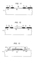
- Fig. 10 shows the substrate prior to flip-chip bonding.
- Conductive runners 67 and 68 form interconnections for the IPD.
- Pad 69 represents a heat sink layer on substrate 11.
- the heat sink layer may also function as part of the electrical circuitry, for example, a ground plane connection for the common ground of the system board. It is preferable to locate the heat sink layer 69 on the same level as bond pads 67 and 68, but alternative arrangements may also be effective. Locating these elements on the same level facilitates the flip-chip bonding arrangement shown, wherein the bond between the heat sink layer on the RF chip and the heat sink layer on the system substrate is made at the same time the IPD substrate is electrically connected to the system board.
- the heat sink layer 69 is preferably approximately coextensive with the RF chip footprint as shown to provide an effective heat sink. Where the heat sink layer serves as a ground plane interconnection it may connect with other circuitry via a surface runner, or may be connected through an interlevel plug to a ground plane at a lower level in a multi-level interconnect substrate.
- FIG. 11 shows a soldermask layer 71 covering the surface of the illustrated portion of the system substrate except for the IPD interconnection sites 73, and the heat sink attachment site 74.
- Fig. 12 shows solder paste 75 applied to the surface of the substrate including the IPD interconnection sites 75 and the heat sink attachment site 77.
- the RP/IPD subassembly of Fig.9 may be flip-chip placed on the system substrate of Fig. 12 and the solder reflowed to effect the attachment.
- Fig. 13 shows the stacked RF/IPD subassembly flip-chip bonded to system substrate 11.
- the heat sink layer 34 on the RF chip 31 is bonded to heat sink layer 69 on substrate 11 for heat sinking. While the assembly shown in Fig. 13 has the advantage of prefabricated underfill, additional underfill may be provided if desired.
- bonds may comprise a simple array of large solder bumps, or balls. Conductive epoxy, etc. may also be substituted for one or more of the bonds.
- the bonds themselves may be referred to herein as bonding bodies, and in the embodiments described here the bonding bodies have a thickness that is approximately equal to the thickness of the RF IC chip (including the heat sink layer on the RF IC chip).
- solder is applied to the RF/IPD chip assembly and the RF/IPD chip assembly is attached to the system substrate by reflowing the solder on the RF/IPD chip assembly.
- solder may be applied first to selected sites on the system substrate and the RF/IPD chip assembly attached to the system substrate by reflowing the solder on the system substrate.
- the RF chip since the RF chip is attached to the substrate in the final assembly, it may be attached to the substrate initially, rather than soldered initially to the IPD device as shown in Fig. 3 .
- the step sequence described in detail above is the preferred embodiment of the invention. As indicated, it results in an intermediate product that is itself a viable commercial product.
- One advantage of this assembly sequence is that the assembled combination of RF chip and IPD can be fully tested prior to mounting on the system substrate. This is not the case for the sequence wherein the RF chip is attached first to the system substrate.
- the dimensions, in particular the thickness, of the RF chip and the bonding layers should be such that the surface of the heat sink layer of RF chip is nearly in contact with the heat sink layer of the system board. Accordingly, to achieve that result, the height of the solder attachments (43 in Fig. 4 ) should be approximately the same as the thickness of the RF chip plus the thickness of the heat sink layer 34.
- the RF chip has a circuit side where the IC is fabricated, and a heat sink side which, according to the invention, has a heat sink layer.
- the circuit side is bonded to the IPD device, and the surface of the heat sink layer is exposed.
- the IPD device is also bonded "upside down" to the system substrate so that when the IPD device is attached to the system substrate the exposed heat sink layer surface of the RF chip is adjacent the heat sink layer on the system substrate to allow direct bonding between them.
- the IC device mounted in the standoff space is an RF power IC chip and the substrate to which the RF chip is attached is an IPD substrate.
- the large substrate may be a semiconductor IC chip, for example, a semiconductor memory or logic chip. Combinations of these IC chips with other IC chips, particularly IC power chips, are potentially attractive. As mentioned earlier, all of these options are intended to be covered in a system wherein the large substrate is an integrated device substrate and the smaller device, mounted in the stand-off, is an IC chip.
Landscapes
- Cooling Or The Like Of Semiconductors Or Solid State Devices (AREA)
- Wire Bonding (AREA)
Applications Claiming Priority (1)
| Application Number | Priority Date | Filing Date | Title |
|---|---|---|---|
| US12/009,805 US20090184416A1 (en) | 2008-01-22 | 2008-01-22 | MCM packages |
Publications (2)
| Publication Number | Publication Date |
|---|---|
| EP2093798A2 true EP2093798A2 (fr) | 2009-08-26 |
| EP2093798A3 EP2093798A3 (fr) | 2012-11-14 |
Family
ID=40791395
Family Applications (1)
| Application Number | Title | Priority Date | Filing Date |
|---|---|---|---|
| EP09151145A Withdrawn EP2093798A3 (fr) | 2008-01-22 | 2009-01-22 | Marche rétractable pour véhicules à moteur |
Country Status (7)
| Country | Link |
|---|---|
| US (1) | US20090184416A1 (fr) |
| EP (1) | EP2093798A3 (fr) |
| JP (1) | JP2009218576A (fr) |
| KR (1) | KR20090080914A (fr) |
| CN (1) | CN101599486A (fr) |
| CA (1) | CA2647863A1 (fr) |
| SG (1) | SG154406A1 (fr) |
Families Citing this family (12)
| Publication number | Priority date | Publication date | Assignee | Title |
|---|---|---|---|---|
| CN101814443B (zh) * | 2010-03-31 | 2011-07-20 | 中国人民解放军国防科学技术大学 | 一种带光接口的高性能处理器多芯片组件芯片设计方法 |
| CN106462788B (zh) * | 2014-03-18 | 2020-07-07 | 惠普发展公司,有限责任合伙企业 | 安全元件 |
| KR102287396B1 (ko) | 2014-10-21 | 2021-08-06 | 삼성전자주식회사 | 시스템 온 패키지 모듈과 이를 포함하는 모바일 컴퓨팅 장치 |
| KR102445515B1 (ko) * | 2017-09-29 | 2022-09-21 | 현대자동차주식회사 | 차량용 전력모듈 |
| US11812545B2 (en) | 2020-01-08 | 2023-11-07 | Delta Electronics (Shanghai) Co., Ltd | Power supply system and electronic device |
| US12342450B2 (en) | 2020-01-08 | 2025-06-24 | Delta Electronics (Shanghai) Co., Ltd | Power supply apparatus, load and electronic device |
| US12610453B2 (en) | 2020-01-08 | 2026-04-21 | Delta Electronics (Shanghai) Co., Ltd. | Vertical power supply system and manufacturing method of connection board |
| CN113097190B (zh) | 2020-01-08 | 2024-08-13 | 台达电子企业管理(上海)有限公司 | 电源模块及电子装置 |
| CN113096933B (zh) | 2020-01-08 | 2022-04-22 | 台达电子企业管理(上海)有限公司 | 多相耦合电感、多相耦合电感阵列及两相反耦合电感 |
| CN113098234B (zh) | 2020-01-08 | 2022-11-01 | 台达电子企业管理(上海)有限公司 | 供电系统 |
| CN112509998A (zh) * | 2020-11-18 | 2021-03-16 | 杰群电子科技(东莞)有限公司 | 一种高功率半导体产品晶圆级封装工艺及半导体产品 |
| CN117174000A (zh) * | 2023-09-19 | 2023-12-05 | 京东方科技集团股份有限公司 | 一种显示模组以及显示装置 |
Citations (1)
| Publication number | Priority date | Publication date | Assignee | Title |
|---|---|---|---|---|
| US5869894A (en) | 1997-07-18 | 1999-02-09 | Lucent Technologies Inc. | RF IC package |
Family Cites Families (10)
| Publication number | Priority date | Publication date | Assignee | Title |
|---|---|---|---|---|
| JP3549294B2 (ja) * | 1995-08-23 | 2004-08-04 | 新光電気工業株式会社 | 半導体装置及びその実装構造 |
| DE19746835A1 (de) * | 1997-10-23 | 1999-05-06 | Jenoptik Jena Gmbh | Verfahren zum Montieren einer einseitig mit einer HR-Schicht beschichteten Laserkristallscheibe auf einen Kühlkörper und verfahrensgemäß hergestellte Schichtanordnung |
| JP2000243467A (ja) * | 1999-02-17 | 2000-09-08 | Toyota Motor Corp | 電子部品基板のはんだ付け方法 |
| JP2001257234A (ja) * | 2000-03-08 | 2001-09-21 | Kobe Steel Ltd | 半導体装置及びその製造方法 |
| US6525413B1 (en) * | 2000-07-12 | 2003-02-25 | Micron Technology, Inc. | Die to die connection method and assemblies and packages including dice so connected |
| US7176506B2 (en) * | 2001-08-28 | 2007-02-13 | Tessera, Inc. | High frequency chip packages with connecting elements |
| JP3768880B2 (ja) * | 2001-12-28 | 2006-04-19 | 松下電器産業株式会社 | フリップチップ実装基板、製造方法及び無線装置 |
| JP3968051B2 (ja) * | 2003-05-14 | 2007-08-29 | 富士通株式会社 | 半導体装置とその製造方法、および半導体装置前駆体とその製造方法 |
| KR100543729B1 (ko) * | 2004-03-24 | 2006-01-20 | 아바고테크놀로지스코리아 주식회사 | 열 방출 효율이 높고 두께는 물론 크기를 감소시킨 고주파모듈 패키지 및 그 조립 방법 |
| US7759793B2 (en) * | 2004-12-13 | 2010-07-20 | Renesas Technology Corp. | Semiconductor device having elastic solder bump to prevent disconnection |
-
2008
- 2008-01-22 US US12/009,805 patent/US20090184416A1/en not_active Abandoned
- 2008-12-19 CA CA002647863A patent/CA2647863A1/fr not_active Abandoned
-
2009
- 2009-01-14 SG SG200900242-9A patent/SG154406A1/en unknown
- 2009-01-20 CN CNA2009100036002A patent/CN101599486A/zh active Pending
- 2009-01-21 KR KR1020090005188A patent/KR20090080914A/ko not_active Withdrawn
- 2009-01-22 JP JP2009011873A patent/JP2009218576A/ja active Pending
- 2009-01-22 EP EP09151145A patent/EP2093798A3/fr not_active Withdrawn
Patent Citations (1)
| Publication number | Priority date | Publication date | Assignee | Title |
|---|---|---|---|---|
| US5869894A (en) | 1997-07-18 | 1999-02-09 | Lucent Technologies Inc. | RF IC package |
Also Published As
| Publication number | Publication date |
|---|---|
| CN101599486A (zh) | 2009-12-09 |
| SG154406A1 (en) | 2009-08-28 |
| KR20090080914A (ko) | 2009-07-27 |
| EP2093798A3 (fr) | 2012-11-14 |
| JP2009218576A (ja) | 2009-09-24 |
| CA2647863A1 (fr) | 2009-07-22 |
| US20090184416A1 (en) | 2009-07-23 |
Similar Documents
| Publication | Publication Date | Title |
|---|---|---|
| EP2093798A2 (fr) | Marche rétractable pour véhicules à moteur | |
| US6214642B1 (en) | Area array stud bump flip chip device and assembly process | |
| US8236608B2 (en) | Stacking package structure with chip embedded inside and die having through silicon via and method of the same | |
| US7898058B2 (en) | Integrated chip package structure using organic substrate and method of manufacturing the same | |
| JP5639368B2 (ja) | スタック式ダイ埋め込み型チップビルドアップのためのシステム及び方法 | |
| JP3481444B2 (ja) | 半導体装置及びその製造方法 | |
| US6642610B2 (en) | Wire bonding method and semiconductor package manufactured using the same | |
| US7173330B2 (en) | Multiple chip semiconductor package | |
| US9129818B2 (en) | Semiconductor device having conductive pads and a method of manufacturing the same | |
| US7338837B2 (en) | Semiconductor packages for enhanced number of terminals, speed and power performance | |
| US20050121765A1 (en) | Multi-chips bumpless assembly package and manufacturing method thereof | |
| TWI280641B (en) | Chip structure | |
| CN105097726A (zh) | 封装结构及封装方法 | |
| US10714408B2 (en) | Semiconductor devices and methods of making semiconductor devices | |
| US8304864B2 (en) | Lead frame routed chip pads for semiconductor packages | |
| CN101276809A (zh) | 半导体器件及其制造方法 | |
| KR20040092411A (ko) | 배선 기판 및 전자 부품 실장 구조 | |
| US20190214367A1 (en) | Stacked package and a manufacturing method of the same | |
| CN120751757A (zh) | 半导体装置及制造半导体装置的方法 | |
| CN107579054A (zh) | 用于半导体封装的连接芯片焊盘的引线框架 | |
| CN1315168C (zh) | 晶圆级封装制作工艺及其晶片结构 | |
| US20260096409A1 (en) | Method of manufacturing an interconnection for an electronic device | |
| CN118156156A (zh) | 封装结构及其形成方法 | |
| JP2007059493A (ja) | 半導体装置およびその製造方法 | |
| KR20100078958A (ko) | 플립 칩 패키지 및 그의 제조방법 |
Legal Events
| Date | Code | Title | Description |
|---|---|---|---|
| PUAI | Public reference made under article 153(3) epc to a published international application that has entered the european phase |
Free format text: ORIGINAL CODE: 0009012 |
|
| AK | Designated contracting states |
Kind code of ref document: A2 Designated state(s): AT BE BG CH CY CZ DE DK EE ES FI FR GB GR HR HU IE IS IT LI LT LU LV MC MK MT NL NO PL PT RO SE SI SK TR |
|
| AX | Request for extension of the european patent |
Extension state: AL BA RS |
|
| RTI1 | Title (correction) |
Free format text: MCM PACKAGES |
|
| PUAL | Search report despatched |
Free format text: ORIGINAL CODE: 0009013 |
|
| AK | Designated contracting states |
Kind code of ref document: A3 Designated state(s): AT BE BG CH CY CZ DE DK EE ES FI FR GB GR HR HU IE IS IT LI LT LU LV MC MK MT NL NO PL PT RO SE SI SK TR |
|
| AX | Request for extension of the european patent |
Extension state: AL BA RS |
|
| RIC1 | Information provided on ipc code assigned before grant |
Ipc: H01L 23/498 20060101ALI20121008BHEP Ipc: H01L 25/16 20060101AFI20121008BHEP Ipc: H01L 25/065 20060101ALI20121008BHEP |
|
| AKY | No designation fees paid | ||
| REG | Reference to a national code |
Ref country code: DE Ref legal event code: R108 |
|
| REG | Reference to a national code |
Ref country code: DE Ref legal event code: R108 Effective date: 20130717 |
|
| STAA | Information on the status of an ep patent application or granted ep patent |
Free format text: STATUS: THE APPLICATION IS DEEMED TO BE WITHDRAWN |
|
| 18D | Application deemed to be withdrawn |
Effective date: 20130515 |