EP2104233A1 - Schaltnetzwerk, variable kondensatorschaltung und ic dafür - Google Patents
Schaltnetzwerk, variable kondensatorschaltung und ic dafür Download PDFInfo
- Publication number
- EP2104233A1 EP2104233A1 EP07829336A EP07829336A EP2104233A1 EP 2104233 A1 EP2104233 A1 EP 2104233A1 EP 07829336 A EP07829336 A EP 07829336A EP 07829336 A EP07829336 A EP 07829336A EP 2104233 A1 EP2104233 A1 EP 2104233A1
- Authority
- EP
- European Patent Office
- Prior art keywords
- fet
- circuit
- drain
- signal
- terminal
- Prior art date
- Legal status (The legal status is an assumption and is not a legal conclusion. Google has not performed a legal analysis and makes no representation as to the accuracy of the status listed.)
- Granted
Links
Images


Classifications
-
- H—ELECTRICITY
- H03—ELECTRONIC CIRCUITRY
- H03K—PULSE TECHNIQUE
- H03K17/00—Electronic switching or gating, i.e. not by contact-making and –breaking
- H03K17/16—Modifications for eliminating interference voltages or currents
- H03K17/161—Modifications for eliminating interference voltages or currents in field-effect transistor switches
- H03K17/162—Modifications for eliminating interference voltages or currents in field-effect transistor switches without feedback from the output circuit to the control circuit
-
- H—ELECTRICITY
- H03—ELECTRONIC CIRCUITRY
- H03K—PULSE TECHNIQUE
- H03K17/00—Electronic switching or gating, i.e. not by contact-making and –breaking
- H03K17/51—Electronic switching or gating, i.e. not by contact-making and –breaking characterised by the components used
- H03K17/56—Electronic switching or gating, i.e. not by contact-making and –breaking characterised by the components used by the use, as active elements, of semiconductor devices
- H03K17/687—Electronic switching or gating, i.e. not by contact-making and –breaking characterised by the components used by the use, as active elements, of semiconductor devices the devices being field-effect transistors
-
- H—ELECTRICITY
- H03—ELECTRONIC CIRCUITRY
- H03K—PULSE TECHNIQUE
- H03K17/00—Electronic switching or gating, i.e. not by contact-making and –breaking
- H03K17/16—Modifications for eliminating interference voltages or currents
- H03K17/161—Modifications for eliminating interference voltages or currents in field-effect transistor switches
- H03K17/165—Modifications for eliminating interference voltages or currents in field-effect transistor switches by feedback from the output circuit to the control circuit
-
- H—ELECTRICITY
- H04—ELECTRIC COMMUNICATION TECHNIQUE
- H04N—PICTORIAL COMMUNICATION, e.g. TELEVISION
- H04N5/00—Details of television systems
- H04N5/44—Receiver circuitry for the reception of television signals according to analogue transmission standards
- H04N5/455—Demodulation-circuits
-
- H—ELECTRICITY
- H03—ELECTRONIC CIRCUITRY
- H03J—TUNING RESONANT CIRCUITS; SELECTING RESONANT CIRCUITS
- H03J2200/00—Indexing scheme relating to tuning resonant circuits and selecting resonant circuits
- H03J2200/10—Tuning of a resonator by means of digitally controlled capacitor bank
-
- H—ELECTRICITY
- H03—ELECTRONIC CIRCUITRY
- H03K—PULSE TECHNIQUE
- H03K2217/00—Indexing scheme related to electronic switching or gating, i.e. not by contact-making or -breaking covered by H03K17/00
- H03K2217/0018—Special modifications or use of the back gate voltage of a FET
Definitions
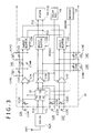
- an oscillation signal of a predetermined frequency is formed by a VCO 31.
- This VCO 31 is for forming a local oscillation signal and forms part of a PLL 30.
- the oscillation signal of the VCO 31 is supplied to a variable dividing circuit 32, by which it is divided into a signal of a frequency of 1/N (N is a positive integer), and this divided signal is supplied as a reference signal to a phase comparison circuit 33.
- a clock (whose frequency is approximately 1 to 2 MHz) is supplied from the outside to a signal formation circuit 34 through the terminal pin T14, and the clock is divided into a signal of a predetermined frequency f34 by the signal formation circuit 34. This frequency signal is supplied as a reference signal to the phase comparison circuit 33.
- the signal components ⁇ cos ⁇ IFt have the same phase while the signal components ⁇ coc ⁇ IFt have the opposite phases to each other.
- the front end circuit 10 shown in FIG. 1 television broadcasts in the frequency band of 46 to 887 MHz as indicated by the items (A) to (C) can be received. Then, at this time, since the center frequency and the pass-band width of the complex band-pass filter 24 are variable, the front end circuit 10 can cope not only with ground wave digital television broadcasts and ground wave analog television broadcasts in Japan but also with digital television broadcasts and analog television broadcasts outside Japan.
- reception of the VL band indicated in the item (A) is permitted, and a channel (frequency) selected by the tuning circuits 12A and 14A is outputted to the nodes P15, P15 and supplied to the mixer circuits 21I and 21Q. And, similar operation is carried out also with regard to the reception bands of the items (B) and (C).
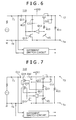
- the FET (Q11) is controlled on/off with the control voltage VG similarly as in the case of FIG. 4 , and the signal of the terminal T2 is controlled on/off in response to the on/off operation.
Landscapes
- Engineering & Computer Science (AREA)
- Multimedia (AREA)
- Signal Processing (AREA)
- Electronic Switches (AREA)
- Amplifiers (AREA)
- Superheterodyne Receivers (AREA)
- Dc-Dc Converters (AREA)
- Networks Using Active Elements (AREA)
Applications Claiming Priority (2)
| Application Number | Priority Date | Filing Date | Title |
|---|---|---|---|
| JP2006349471A JP5151145B2 (ja) | 2006-12-26 | 2006-12-26 | スイッチ回路、可変コンデンサ回路およびそのic |
| PCT/JP2007/069598 WO2008078443A1 (ja) | 2006-12-26 | 2007-10-05 | スイッチ回路、可変コンデンサ回路およびそのic |
Publications (3)
| Publication Number | Publication Date |
|---|---|
| EP2104233A1 true EP2104233A1 (de) | 2009-09-23 |
| EP2104233A4 EP2104233A4 (de) | 2010-10-13 |
| EP2104233B1 EP2104233B1 (de) | 2014-04-02 |
Family
ID=39562237
Family Applications (1)
| Application Number | Title | Priority Date | Filing Date |
|---|---|---|---|
| EP07829336.2A Not-in-force EP2104233B1 (de) | 2006-12-26 | 2007-10-05 | Schaltnetzwerk, variable kondensatorschaltung und ic dafür |
Country Status (7)
| Country | Link |
|---|---|
| US (1) | US7944268B2 (de) |
| EP (1) | EP2104233B1 (de) |
| JP (1) | JP5151145B2 (de) |
| KR (1) | KR101407382B1 (de) |
| CN (1) | CN101578766B (de) |
| TW (1) | TW200838165A (de) |
| WO (1) | WO2008078443A1 (de) |
Families Citing this family (13)
| Publication number | Priority date | Publication date | Assignee | Title |
|---|---|---|---|---|
| JP5301299B2 (ja) * | 2008-01-31 | 2013-09-25 | 株式会社半導体エネルギー研究所 | 半導体装置 |
| JP4859902B2 (ja) * | 2008-10-01 | 2012-01-25 | 株式会社豊田中央研究所 | ホールド回路 |
| ATE545202T1 (de) * | 2009-03-03 | 2012-02-15 | St Microelectronics Grenoble | Analogschalter |
| JP5251953B2 (ja) * | 2010-09-30 | 2013-07-31 | 株式会社村田製作所 | スイッチ回路、半導体装置及び携帯無線機 |
| US8575990B2 (en) | 2011-10-14 | 2013-11-05 | Silicon Power Corporation | Matrix-stages solid state ultrafast switch |
| JP6184057B2 (ja) * | 2012-04-18 | 2017-08-23 | ルネサスエレクトロニクス株式会社 | 半導体装置 |
| TWI489776B (zh) * | 2012-05-31 | 2015-06-21 | Richwave Technology Corp | Rf開關之電容補償電路 |
| US9432007B1 (en) * | 2014-08-15 | 2016-08-30 | Xilinx, Inc. | Out-of-band (OOB) detection circuit for serial/deserializer (SERDES) |
| US10270427B2 (en) * | 2015-12-07 | 2019-04-23 | Qorvo International Pte. Ltd. | On-chip balun circuit and multi-port antenna switch circuit |
| US20170279445A1 (en) * | 2016-03-24 | 2017-09-28 | Qualcomm Incorporated | Area-efficient differential switched capacitors |
| DE102016110344A1 (de) * | 2016-06-03 | 2017-12-07 | Infineon Technologies Ag | Rf-empfänger mit eingebauter selbsttestfunktion |
| CN108919728B (zh) * | 2018-08-23 | 2023-09-26 | 深圳和而泰智能控制股份有限公司 | 一种控制电路 |
| US10917132B1 (en) * | 2019-07-10 | 2021-02-09 | Rockwell Collins, Inc. | Switchless transceiver integrated programmable differential topology |
Family Cites Families (34)
| Publication number | Priority date | Publication date | Assignee | Title |
|---|---|---|---|---|
| JPS57173228A (en) * | 1981-04-20 | 1982-10-25 | Hitachi Ltd | Mos-fet switch |
| US5444219A (en) * | 1990-09-24 | 1995-08-22 | U.S. Philips Corporation | Temperature sensing device and a temperature sensing circuit using such a device |
| US5223754A (en) * | 1990-12-14 | 1993-06-29 | Massachusetts Institute Of Technology | Resistive fuse circuits for image segmentation and smoothing |
| JP3169775B2 (ja) * | 1994-08-29 | 2001-05-28 | 株式会社日立製作所 | 半導体回路、スイッチ及びそれを用いた通信機 |
| JPH08223020A (ja) | 1995-02-10 | 1996-08-30 | Kenwood Corp | 信号切換回路 |
| JPH10284714A (ja) | 1997-04-07 | 1998-10-23 | Toshiba Corp | 固体撮像装置及びこれを用いた撮像システム |
| JP2000124783A (ja) * | 1998-10-13 | 2000-04-28 | Toshiba Corp | 半導体高周波切替回路 |
| US6727521B2 (en) | 2000-09-25 | 2004-04-27 | Foveon, Inc. | Vertical color filter detector group and array |
| US6396325B2 (en) | 1999-12-03 | 2002-05-28 | Fairchild Semiconductor Corporation | High frequency MOSFET switch |
| WO2001067602A2 (en) * | 2000-03-03 | 2001-09-13 | Alpha Industries, Inc. | Electronic switch |
| WO2002017504A1 (en) * | 2000-08-22 | 2002-02-28 | Hitachi Metals, Ltd. | Laminated high-frequency switch module |
| JP2002185300A (ja) * | 2000-12-15 | 2002-06-28 | Fujitsu Ltd | 終端抵抗回路および信号伝送システム |
| US6509757B1 (en) | 2001-08-02 | 2003-01-21 | Agilent Technologies, Inc. | Binary weighted thermometer code for PVT controlled output drivers |
| US6889036B2 (en) * | 2002-03-07 | 2005-05-03 | Freescale Semiconductor, Inc. | Integrated frequency selectable resonant coupling network and method thereof |
| WO2003079566A2 (en) * | 2002-03-11 | 2003-09-25 | Fairchild Semiconductor Corporation | Drain activated/deactivated ac coupled bandpass rf switch |
| US6998660B2 (en) | 2002-03-20 | 2006-02-14 | Foveon, Inc. | Vertical color filter sensor group array that emulates a pattern of single-layer sensors with efficient use of each sensor group's sensors |
| US6946715B2 (en) | 2003-02-19 | 2005-09-20 | Micron Technology, Inc. | CMOS image sensor and method of fabrication |
| JP3849600B2 (ja) * | 2002-07-12 | 2006-11-22 | 日本電気株式会社 | 高周波スイッチ |
| US6975271B2 (en) * | 2003-02-26 | 2005-12-13 | Matsushita Electric Industrial Co., Ltd. | Antenna switch module, all-in-one communication module, communication apparatus and method for manufacturing antenna switch module |
| US20040263234A1 (en) * | 2003-06-26 | 2004-12-30 | International Business Machines Corporation | Arrangement, network and method for reducing non-linearity within active resistor networks |
| US7098755B2 (en) | 2003-07-16 | 2006-08-29 | Analog Devices, Inc. | High power, high linearity and low insertion loss single pole double throw transmitter/receiver switch |
| JP3910568B2 (ja) * | 2003-08-14 | 2007-04-25 | 富士通株式会社 | レベルダウンコンバータ |
| US20050040909A1 (en) * | 2003-08-20 | 2005-02-24 | Waight Matthew Glenn | Broadband integrated digitally tunable filters |
| US7116183B2 (en) * | 2004-02-05 | 2006-10-03 | Qualcomm Incorporated | Temperature compensated voltage controlled oscillator |
| US7084713B2 (en) * | 2004-03-29 | 2006-08-01 | Qualcomm Inc. | Programmable capacitor bank for a voltage controlled oscillator |
| CN1943002A (zh) | 2004-05-27 | 2007-04-04 | 通用电气公司 | 对物件进行等离子体处理的装置和方法 |
| JP2006094206A (ja) * | 2004-09-24 | 2006-04-06 | Toshiba Corp | 高周波スイッチ回路及び半導体装置 |
| ES2263357B1 (es) | 2004-11-16 | 2007-11-16 | Diseño De Sistemas En Silicio, S.A. | Circuito conmutador para la obtencion de un rango dinamico duplicado. |
| JP2006332416A (ja) | 2005-05-27 | 2006-12-07 | Nec Electronics Corp | 半導体装置 |
| US7608874B2 (en) | 2006-03-17 | 2009-10-27 | Sharp Laboratories Of America, Inc. | Fully isolated photodiode stack |
| KR100827447B1 (ko) | 2007-01-24 | 2008-05-06 | 삼성전자주식회사 | 이미지 센서와 그 제조 방법 및 이미지 센싱 방법 |
| US8115242B2 (en) | 2007-02-07 | 2012-02-14 | Foveon, Inc. | Pinned photodiode CMOS pixel sensor |
| US7710181B2 (en) * | 2007-08-20 | 2010-05-04 | Panasonic Corporation | Variable attenuator and wireless communication device |
| TWI348270B (en) * | 2008-05-21 | 2011-09-01 | Niko Semiconductor Co Ltd | A negative voltage switching apparatus |
-
2006
- 2006-12-26 JP JP2006349471A patent/JP5151145B2/ja not_active Expired - Fee Related
-
2007
- 2007-10-05 WO PCT/JP2007/069598 patent/WO2008078443A1/ja not_active Ceased
- 2007-10-05 KR KR1020097012910A patent/KR101407382B1/ko not_active Expired - Fee Related
- 2007-10-05 US US12/521,085 patent/US7944268B2/en not_active Expired - Fee Related
- 2007-10-05 EP EP07829336.2A patent/EP2104233B1/de not_active Not-in-force
- 2007-10-05 CN CN2007800483772A patent/CN101578766B/zh not_active Expired - Fee Related
- 2007-12-14 TW TW096148078A patent/TW200838165A/zh not_active IP Right Cessation
Also Published As
| Publication number | Publication date |
|---|---|
| EP2104233B1 (de) | 2014-04-02 |
| US20100085109A1 (en) | 2010-04-08 |
| JP2008160673A (ja) | 2008-07-10 |
| KR20090094291A (ko) | 2009-09-04 |
| TWI371173B (de) | 2012-08-21 |
| TW200838165A (en) | 2008-09-16 |
| WO2008078443A1 (ja) | 2008-07-03 |
| US7944268B2 (en) | 2011-05-17 |
| CN101578766A (zh) | 2009-11-11 |
| KR101407382B1 (ko) | 2014-06-13 |
| JP5151145B2 (ja) | 2013-02-27 |
| EP2104233A4 (de) | 2010-10-13 |
| CN101578766B (zh) | 2012-04-25 |
Similar Documents
| Publication | Publication Date | Title |
|---|---|---|
| EP2104233B1 (de) | Schaltnetzwerk, variable kondensatorschaltung und ic dafür | |
| EP2128993B1 (de) | Frontend-schaltung | |
| JP4269188B2 (ja) | 可変利得増幅回路、受信機および受信機用ic | |
| KR20090020700A (ko) | 신호들의 수동 증폭 | |
| US8212420B2 (en) | Variable capacitance circuit | |
| JP4710849B2 (ja) | 増幅回路、受信機および受信機用ic | |
| US9564858B2 (en) | Parallel resonant circuit | |
| US6788922B2 (en) | Radio FM receiver having a frequency 2-divider and a frequency 3-divider for alternatively dividing a VCO signal for down-converting a received radio signal | |
| US9432609B2 (en) | Signal processing device and signal processing method | |
| JP2008160672A (ja) | ミキサ回路の入力回路 | |
| US7787851B2 (en) | Circuit arrangement with radio-frequency mixer, and receiver arrangement with the circuit arrangement | |
| JP4899992B2 (ja) | フロントエンド集積回路 | |
| JPH01213007A (ja) | ミクサ回路 | |
| JPH09107270A (ja) | アナログ遅延回路 | |
| JP2008227662A (ja) | 検出回路および利得制御回路 |
Legal Events
| Date | Code | Title | Description |
|---|---|---|---|
| PUAI | Public reference made under article 153(3) epc to a published international application that has entered the european phase |
Free format text: ORIGINAL CODE: 0009012 |
|
| 17P | Request for examination filed |
Effective date: 20090624 |
|
| AK | Designated contracting states |
Kind code of ref document: A1 Designated state(s): AT BE BG CH CY CZ DE DK EE ES FI FR GB GR HU IE IS IT LI LT LU LV MC MT NL PL PT RO SE SI SK TR |
|
| DAX | Request for extension of the european patent (deleted) | ||
| A4 | Supplementary search report drawn up and despatched |
Effective date: 20100909 |
|
| 17Q | First examination report despatched |
Effective date: 20100917 |
|
| GRAP | Despatch of communication of intention to grant a patent |
Free format text: ORIGINAL CODE: EPIDOSNIGR1 |
|
| INTG | Intention to grant announced |
Effective date: 20131015 |
|
| GRAS | Grant fee paid |
Free format text: ORIGINAL CODE: EPIDOSNIGR3 |
|
| GRAA | (expected) grant |
Free format text: ORIGINAL CODE: 0009210 |
|
| AK | Designated contracting states |
Kind code of ref document: B1 Designated state(s): AT BE BG CH CY CZ DE DK EE ES FI FR GB GR HU IE IS IT LI LT LU LV MC MT NL PL PT RO SE SI SK TR |
|
| REG | Reference to a national code |
Ref country code: GB Ref legal event code: FG4D |
|
| REG | Reference to a national code |
Ref country code: AT Ref legal event code: REF Ref document number: 660665 Country of ref document: AT Kind code of ref document: T Effective date: 20140415 Ref country code: CH Ref legal event code: EP |
|
| REG | Reference to a national code |
Ref country code: IE Ref legal event code: FG4D |
|
| REG | Reference to a national code |
Ref country code: DE Ref legal event code: R096 Ref document number: 602007035932 Country of ref document: DE Effective date: 20140515 |
|
| REG | Reference to a national code |
Ref country code: AT Ref legal event code: MK05 Ref document number: 660665 Country of ref document: AT Kind code of ref document: T Effective date: 20140402 |
|
| REG | Reference to a national code |
Ref country code: NL Ref legal event code: VDEP Effective date: 20140402 |
|
| REG | Reference to a national code |
Ref country code: LT Ref legal event code: MG4D |
|
| PG25 | Lapsed in a contracting state [announced via postgrant information from national office to epo] |
Ref country code: BG Free format text: LAPSE BECAUSE OF FAILURE TO SUBMIT A TRANSLATION OF THE DESCRIPTION OR TO PAY THE FEE WITHIN THE PRESCRIBED TIME-LIMIT Effective date: 20140702 Ref country code: LT Free format text: LAPSE BECAUSE OF FAILURE TO SUBMIT A TRANSLATION OF THE DESCRIPTION OR TO PAY THE FEE WITHIN THE PRESCRIBED TIME-LIMIT Effective date: 20140402 Ref country code: CZ Free format text: LAPSE BECAUSE OF FAILURE TO SUBMIT A TRANSLATION OF THE DESCRIPTION OR TO PAY THE FEE WITHIN THE PRESCRIBED TIME-LIMIT Effective date: 20140402 Ref country code: NL Free format text: LAPSE BECAUSE OF FAILURE TO SUBMIT A TRANSLATION OF THE DESCRIPTION OR TO PAY THE FEE WITHIN THE PRESCRIBED TIME-LIMIT Effective date: 20140402 Ref country code: CY Free format text: LAPSE BECAUSE OF FAILURE TO SUBMIT A TRANSLATION OF THE DESCRIPTION OR TO PAY THE FEE WITHIN THE PRESCRIBED TIME-LIMIT Effective date: 20140402 Ref country code: GR Free format text: LAPSE BECAUSE OF FAILURE TO SUBMIT A TRANSLATION OF THE DESCRIPTION OR TO PAY THE FEE WITHIN THE PRESCRIBED TIME-LIMIT Effective date: 20140703 Ref country code: FI Free format text: LAPSE BECAUSE OF FAILURE TO SUBMIT A TRANSLATION OF THE DESCRIPTION OR TO PAY THE FEE WITHIN THE PRESCRIBED TIME-LIMIT Effective date: 20140402 Ref country code: IS Free format text: LAPSE BECAUSE OF FAILURE TO SUBMIT A TRANSLATION OF THE DESCRIPTION OR TO PAY THE FEE WITHIN THE PRESCRIBED TIME-LIMIT Effective date: 20140802 |
|
| PG25 | Lapsed in a contracting state [announced via postgrant information from national office to epo] |
Ref country code: SE Free format text: LAPSE BECAUSE OF FAILURE TO SUBMIT A TRANSLATION OF THE DESCRIPTION OR TO PAY THE FEE WITHIN THE PRESCRIBED TIME-LIMIT Effective date: 20140402 Ref country code: ES Free format text: LAPSE BECAUSE OF FAILURE TO SUBMIT A TRANSLATION OF THE DESCRIPTION OR TO PAY THE FEE WITHIN THE PRESCRIBED TIME-LIMIT Effective date: 20140402 Ref country code: LV Free format text: LAPSE BECAUSE OF FAILURE TO SUBMIT A TRANSLATION OF THE DESCRIPTION OR TO PAY THE FEE WITHIN THE PRESCRIBED TIME-LIMIT Effective date: 20140402 Ref country code: PL Free format text: LAPSE BECAUSE OF FAILURE TO SUBMIT A TRANSLATION OF THE DESCRIPTION OR TO PAY THE FEE WITHIN THE PRESCRIBED TIME-LIMIT Effective date: 20140402 Ref country code: AT Free format text: LAPSE BECAUSE OF FAILURE TO SUBMIT A TRANSLATION OF THE DESCRIPTION OR TO PAY THE FEE WITHIN THE PRESCRIBED TIME-LIMIT Effective date: 20140402 |
|
| PG25 | Lapsed in a contracting state [announced via postgrant information from national office to epo] |
Ref country code: PT Free format text: LAPSE BECAUSE OF FAILURE TO SUBMIT A TRANSLATION OF THE DESCRIPTION OR TO PAY THE FEE WITHIN THE PRESCRIBED TIME-LIMIT Effective date: 20140804 |
|
| REG | Reference to a national code |
Ref country code: DE Ref legal event code: R097 Ref document number: 602007035932 Country of ref document: DE |
|
| PG25 | Lapsed in a contracting state [announced via postgrant information from national office to epo] |
Ref country code: EE Free format text: LAPSE BECAUSE OF FAILURE TO SUBMIT A TRANSLATION OF THE DESCRIPTION OR TO PAY THE FEE WITHIN THE PRESCRIBED TIME-LIMIT Effective date: 20140402 Ref country code: DK Free format text: LAPSE BECAUSE OF FAILURE TO SUBMIT A TRANSLATION OF THE DESCRIPTION OR TO PAY THE FEE WITHIN THE PRESCRIBED TIME-LIMIT Effective date: 20140402 Ref country code: BE Free format text: LAPSE BECAUSE OF FAILURE TO SUBMIT A TRANSLATION OF THE DESCRIPTION OR TO PAY THE FEE WITHIN THE PRESCRIBED TIME-LIMIT Effective date: 20140402 Ref country code: SK Free format text: LAPSE BECAUSE OF FAILURE TO SUBMIT A TRANSLATION OF THE DESCRIPTION OR TO PAY THE FEE WITHIN THE PRESCRIBED TIME-LIMIT Effective date: 20140402 Ref country code: RO Free format text: LAPSE BECAUSE OF FAILURE TO SUBMIT A TRANSLATION OF THE DESCRIPTION OR TO PAY THE FEE WITHIN THE PRESCRIBED TIME-LIMIT Effective date: 20140402 |
|
| PLBE | No opposition filed within time limit |
Free format text: ORIGINAL CODE: 0009261 |
|
| STAA | Information on the status of an ep patent application or granted ep patent |
Free format text: STATUS: NO OPPOSITION FILED WITHIN TIME LIMIT |
|
| 26N | No opposition filed |
Effective date: 20150106 |
|
| PG25 | Lapsed in a contracting state [announced via postgrant information from national office to epo] |
Ref country code: IT Free format text: LAPSE BECAUSE OF FAILURE TO SUBMIT A TRANSLATION OF THE DESCRIPTION OR TO PAY THE FEE WITHIN THE PRESCRIBED TIME-LIMIT Effective date: 20140402 |
|
| REG | Reference to a national code |
Ref country code: DE Ref legal event code: R084 Ref document number: 602007035932 Country of ref document: DE |
|
| REG | Reference to a national code |
Ref country code: DE Ref legal event code: R097 Ref document number: 602007035932 Country of ref document: DE Effective date: 20150106 |
|
| REG | Reference to a national code |
Ref country code: GB Ref legal event code: 746 Effective date: 20150421 |
|
| REG | Reference to a national code |
Ref country code: DE Ref legal event code: R084 Ref document number: 602007035932 Country of ref document: DE Effective date: 20150410 |
|
| PG25 | Lapsed in a contracting state [announced via postgrant information from national office to epo] |
Ref country code: MC Free format text: LAPSE BECAUSE OF FAILURE TO SUBMIT A TRANSLATION OF THE DESCRIPTION OR TO PAY THE FEE WITHIN THE PRESCRIBED TIME-LIMIT Effective date: 20140402 Ref country code: LU Free format text: LAPSE BECAUSE OF FAILURE TO SUBMIT A TRANSLATION OF THE DESCRIPTION OR TO PAY THE FEE WITHIN THE PRESCRIBED TIME-LIMIT Effective date: 20141005 |
|
| REG | Reference to a national code |
Ref country code: CH Ref legal event code: PL |
|
| REG | Reference to a national code |
Ref country code: IE Ref legal event code: MM4A |
|
| PG25 | Lapsed in a contracting state [announced via postgrant information from national office to epo] |
Ref country code: LI Free format text: LAPSE BECAUSE OF NON-PAYMENT OF DUE FEES Effective date: 20141031 Ref country code: SI Free format text: LAPSE BECAUSE OF FAILURE TO SUBMIT A TRANSLATION OF THE DESCRIPTION OR TO PAY THE FEE WITHIN THE PRESCRIBED TIME-LIMIT Effective date: 20140402 Ref country code: CH Free format text: LAPSE BECAUSE OF NON-PAYMENT OF DUE FEES Effective date: 20141031 |
|
| REG | Reference to a national code |
Ref country code: FR Ref legal event code: PLFP Year of fee payment: 9 |
|
| PG25 | Lapsed in a contracting state [announced via postgrant information from national office to epo] |
Ref country code: IE Free format text: LAPSE BECAUSE OF NON-PAYMENT OF DUE FEES Effective date: 20141005 |
|
| PG25 | Lapsed in a contracting state [announced via postgrant information from national office to epo] |
Ref country code: HU Free format text: LAPSE BECAUSE OF FAILURE TO SUBMIT A TRANSLATION OF THE DESCRIPTION OR TO PAY THE FEE WITHIN THE PRESCRIBED TIME-LIMIT; INVALID AB INITIO Effective date: 20071005 Ref country code: TR Free format text: LAPSE BECAUSE OF FAILURE TO SUBMIT A TRANSLATION OF THE DESCRIPTION OR TO PAY THE FEE WITHIN THE PRESCRIBED TIME-LIMIT Effective date: 20140402 Ref country code: MT Free format text: LAPSE BECAUSE OF FAILURE TO SUBMIT A TRANSLATION OF THE DESCRIPTION OR TO PAY THE FEE WITHIN THE PRESCRIBED TIME-LIMIT Effective date: 20140402 |
|
| REG | Reference to a national code |
Ref country code: FR Ref legal event code: PLFP Year of fee payment: 10 |
|
| REG | Reference to a national code |
Ref country code: FR Ref legal event code: PLFP Year of fee payment: 11 |
|
| REG | Reference to a national code |
Ref country code: FR Ref legal event code: PLFP Year of fee payment: 12 |
|
| PGFP | Annual fee paid to national office [announced via postgrant information from national office to epo] |
Ref country code: DE Payment date: 20201022 Year of fee payment: 14 Ref country code: GB Payment date: 20201022 Year of fee payment: 14 Ref country code: FR Payment date: 20201022 Year of fee payment: 14 |
|
| REG | Reference to a national code |
Ref country code: DE Ref legal event code: R119 Ref document number: 602007035932 Country of ref document: DE |
|
| GBPC | Gb: european patent ceased through non-payment of renewal fee |
Effective date: 20211005 |
|
| PG25 | Lapsed in a contracting state [announced via postgrant information from national office to epo] |
Ref country code: GB Free format text: LAPSE BECAUSE OF NON-PAYMENT OF DUE FEES Effective date: 20211005 Ref country code: DE Free format text: LAPSE BECAUSE OF NON-PAYMENT OF DUE FEES Effective date: 20220503 |
|
| PG25 | Lapsed in a contracting state [announced via postgrant information from national office to epo] |
Ref country code: FR Free format text: LAPSE BECAUSE OF NON-PAYMENT OF DUE FEES Effective date: 20211031 |