EP2109155A2 - Cellule solaire à film mince en silicium et son procédé de fabrication - Google Patents
Cellule solaire à film mince en silicium et son procédé de fabrication Download PDFInfo
- Publication number
- EP2109155A2 EP2109155A2 EP09157764A EP09157764A EP2109155A2 EP 2109155 A2 EP2109155 A2 EP 2109155A2 EP 09157764 A EP09157764 A EP 09157764A EP 09157764 A EP09157764 A EP 09157764A EP 2109155 A2 EP2109155 A2 EP 2109155A2
- Authority
- EP
- European Patent Office
- Prior art keywords
- layer
- type
- type window
- window layer
- buffer layer
- Prior art date
- Legal status (The legal status is an assumption and is not a legal conclusion. Google has not performed a legal analysis and makes no representation as to the accuracy of the status listed.)
- Withdrawn
Links
Images


Classifications
-
- H—ELECTRICITY
- H10—SEMICONDUCTOR DEVICES; ELECTRIC SOLID-STATE DEVICES NOT OTHERWISE PROVIDED FOR
- H10F—INORGANIC SEMICONDUCTOR DEVICES SENSITIVE TO INFRARED RADIATION, LIGHT, ELECTROMAGNETIC RADIATION OF SHORTER WAVELENGTH OR CORPUSCULAR RADIATION
- H10F10/00—Individual photovoltaic cells, e.g. solar cells
- H10F10/10—Individual photovoltaic cells, e.g. solar cells having potential barriers
- H10F10/17—Photovoltaic cells having only PIN junction potential barriers
-
- H—ELECTRICITY
- H10—SEMICONDUCTOR DEVICES; ELECTRIC SOLID-STATE DEVICES NOT OTHERWISE PROVIDED FOR
- H10F—INORGANIC SEMICONDUCTOR DEVICES SENSITIVE TO INFRARED RADIATION, LIGHT, ELECTROMAGNETIC RADIATION OF SHORTER WAVELENGTH OR CORPUSCULAR RADIATION
- H10F10/00—Individual photovoltaic cells, e.g. solar cells
- H10F10/10—Individual photovoltaic cells, e.g. solar cells having potential barriers
- H10F10/16—Photovoltaic cells having only PN heterojunction potential barriers
- H10F10/164—Photovoltaic cells having only PN heterojunction potential barriers comprising heterojunctions with Group IV materials, e.g. ITO/Si or GaAs/SiGe photovoltaic cells
- H10F10/165—Photovoltaic cells having only PN heterojunction potential barriers comprising heterojunctions with Group IV materials, e.g. ITO/Si or GaAs/SiGe photovoltaic cells the heterojunctions being Group IV-IV heterojunctions, e.g. Si/Ge, SiGe/Si or Si/SiC photovoltaic cells
-
- H—ELECTRICITY
- H10—SEMICONDUCTOR DEVICES; ELECTRIC SOLID-STATE DEVICES NOT OTHERWISE PROVIDED FOR
- H10F—INORGANIC SEMICONDUCTOR DEVICES SENSITIVE TO INFRARED RADIATION, LIGHT, ELECTROMAGNETIC RADIATION OF SHORTER WAVELENGTH OR CORPUSCULAR RADIATION
- H10F10/00—Individual photovoltaic cells, e.g. solar cells
- H10F10/10—Individual photovoltaic cells, e.g. solar cells having potential barriers
- H10F10/17—Photovoltaic cells having only PIN junction potential barriers
- H10F10/172—Photovoltaic cells having only PIN junction potential barriers comprising multiple PIN junctions, e.g. tandem cells
-
- H—ELECTRICITY
- H10—SEMICONDUCTOR DEVICES; ELECTRIC SOLID-STATE DEVICES NOT OTHERWISE PROVIDED FOR
- H10F—INORGANIC SEMICONDUCTOR DEVICES SENSITIVE TO INFRARED RADIATION, LIGHT, ELECTROMAGNETIC RADIATION OF SHORTER WAVELENGTH OR CORPUSCULAR RADIATION
- H10F71/00—Manufacture or treatment of devices covered by this subclass
-
- H—ELECTRICITY
- H10—SEMICONDUCTOR DEVICES; ELECTRIC SOLID-STATE DEVICES NOT OTHERWISE PROVIDED FOR
- H10F—INORGANIC SEMICONDUCTOR DEVICES SENSITIVE TO INFRARED RADIATION, LIGHT, ELECTROMAGNETIC RADIATION OF SHORTER WAVELENGTH OR CORPUSCULAR RADIATION
- H10F71/00—Manufacture or treatment of devices covered by this subclass
- H10F71/121—The active layers comprising only Group IV materials
- H10F71/1215—The active layers comprising only Group IV materials comprising at least two Group IV elements, e.g. SiGe
-
- Y—GENERAL TAGGING OF NEW TECHNOLOGICAL DEVELOPMENTS; GENERAL TAGGING OF CROSS-SECTIONAL TECHNOLOGIES SPANNING OVER SEVERAL SECTIONS OF THE IPC; TECHNICAL SUBJECTS COVERED BY FORMER USPC CROSS-REFERENCE ART COLLECTIONS [XRACs] AND DIGESTS
- Y02—TECHNOLOGIES OR APPLICATIONS FOR MITIGATION OR ADAPTATION AGAINST CLIMATE CHANGE
- Y02E—REDUCTION OF GREENHOUSE GAS [GHG] EMISSIONS, RELATED TO ENERGY GENERATION, TRANSMISSION OR DISTRIBUTION
- Y02E10/00—Energy generation through renewable energy sources
- Y02E10/50—Photovoltaic [PV] energy
- Y02E10/548—Amorphous silicon PV cells
Definitions
- the embodiment relates to a thin film silicon solar cell and manufacturing method thereof.
- Hydrogenated amorphous silicon (a-Si) solar cells have been widely studied due to high photosensitivity in a visible light region, easy control of an optical band gap, cost effective, low temperature, and large area process possibility. Further, there have been many attempts to reduce Stabler-Wronski effect of amorphous silicon materials. As a result, methods for diluting a silane (SiH 4 ) with hydrogen (H 2 ) have been developed.
- the p-type window layer should have a wide optical band gap and high electric conductivity.
- a p-type window forming hetero-junction at the interface between the p-type window layer and an i-type absorber layer has been widely used.
- an abrupt optical band gap difference at hetero-junction interface between the p-type window layer and the i-type absorber layer increases a defect density at the interface, and thereby causing recombination loss.
- carbon is introduced to the p-type window layer to enhance the optical band gap , it limits the overall cell performance due to a high series resistance.
- a graded band gap i-a-SiC:H buffer layer manufactured by gradually reducing carbon content, and inserted it at the interface between a p-type window layer and an i-type absorber layer (p-a-SiC:H/i-a-Si:H) in 1984.
- U.S.A. Solarax corporation developed an amorphous silicon (a-Si:H) solar cell in which a graded band gap i-a-SiC:H buffer layer is inserted by plasma-enhanced chemical vapor deposition (PECVD).
- PECVD plasma-enhanced chemical vapor deposition
- Tokyo Institute of Technology also developed a thin film silicon solar cell with a structure of glass/SnO2/p-a-SiC:H/graded band gap i-a-SiC:H/i-a-Si:H/n- ⁇ c-Si:H/Ag structure (area: 0.09 cm 2 ) by photo-CVD.
- graded band gap i-a-SiC:H buffer layer deposited without hydrogenated dilution has a large dangling bond defect density, recombination loss at the interface between the p-type window layer and the i-type absorber layer is still high.
- the graded band gap i-a-SiC:H buffer layer has a disadvantage that efficiency of a solar cell is reduced due to a low electric conductivity thereof.
- the double p-a-SiC:H structure minimizes light absorption in a p-type window layer, and effectively reduces recombination at the interface between a p-type window layer and an i-type absorber layer, and thereby improving efficiency of a solar cell based on a p-i-n type amorphous silicon.
- the photo-CVD method since the photo-CVD method has a low deposition rate and a thin film is coated on a quartz window transmitting ultraviolet light during deposition, after a vacuum of a chamber is broken and the thin film is removed from the quartz window, the chamber should be baked in order to again maintain high vacuum. Thus, it takes long time to produce the solar cell. Accordingly, the photo-CVD method is not suitable for mass production of the solar cell.
- a thin film silicon solar cell comprises a front transparent electrode stacked on a transparent substrate, a p-type window layer stacked on the front transparent electrode, and having a thickness in a range of 12 nm to 17 nm, a buffer layer stacked on the p-type window layer, having a carbon concentration in a range of 0.5 to 3.0 atomic % and a thickness in a range of 3 to 8 nm, an i-type absorber layer stacked on the buffer layer, an n-type layer stacked on the i-type absorber layer, and a metal rear electrode stacked on the n-type layer.
- the buffer layer may include a hydrogenated amorphous silicon carbide.
- the p-type window layer may have an electric conductivity of 1x10⁻⁶ S/cm.
- the p-type window layer may include a hydrogenated amorphous silicon carbide.
- the p-type window layer may have a constant optical band gap.
- a method for manufacturing a thin film silicon solar cell comprises stacking a front transparent electrode on a transparent substrate, stacking a p-type window layer on the front transparent electrode to have a silane concentration in a range of 5 to 10 % and a thickness in a range of 12 nm to 17 nm, stacking a buffer layer stacked on the p-type window layer to have a silane concentration in a range of 0.5 to 5 % and a thickness in a range of 3 to 8 nm, stacking an i-type absorber layer on the buffer layer, stacking an n-type layer on the i-type absorber layer and stacking a metal rear electrode on the n-type layer.
- the buffer layer may be formed by a flow rate ratio of a boron source gas ranging from 100 to 2000 ppm in the step of stacking the buffer layer.
- the buffer layer may have a carbon concentration in a range of 0.5 to 3.0 atomic %.
- the p-type window layer and the buffer layer may be formed by reaction gas comprising silane (SiH 4 ), hydrogen (H 2 ), boron source gas, and carbon source gas.
- a temperature of the transparent substrate may range from 100 to 200 ⁇ during deposition of the p-type window layer.
- a base pressure of a reaction chamber may range from 10 -7 to 10 -5 Torr during deposition of the p-type window layer.
- a deposition pressure of a reaction chamber may range from 0.4 to 2 Torr during deposition of the p-type window layer.
- the p-type window layer may have an electric conductivity of 1x10 -6 S/cm.
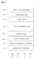
- FIG. 1 is a cross-sectional view illustrating a single junction pi-n type amorphous thin film silicon solar cell in accordance with an embodiment
- FIG. 2 is a flow chart illustrating a method for manufacturing a thin film silicon solar cell in accordance with an embodiment
- FIG. 3 is a flow chart illustrating a formation procedure of a p-type window layer in the manufacturing method shown in FIG. 2 ;
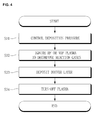
- FIG. 4 is a flow chart illustrating a formation procedure of a buffer layer in the manufacturing method shown in FIG. 2 .
- a thin film silicon solar cell according to the present embodiment has a structure in which a plurality of unit cells are electrically connected to each other in serial on a transparent substrate 10 such as a glass substrate or a transparent plastic substrate.
- FIG. 1 is a cross-sectional view illustrating a single junction pi-n type amorphous thin film silicon solar cell in accordance with an embodiment.
- a thin film silicon solar cell includes a front transparent electrode 20 which is formed on a transparent substrate 10 and on which a surface texture is formed; an amorphous silicon carbide (p-a-SiC:H) window layer 30a (referred to as 'p-type window layer' hereinafter) low diluted with hydrogen on the front transparent electrode 20; an amorphous silicon carbide (p-a-SiC:H) buffer layer 30b (referred to as 'buffer layer' hereinafter) more highly diluted with hydrogen on the p-type window layer 30a than the hydrogen dilution of the p-type window layer 30a; and an i-type absorber layer 40, an n-type layer 50, a back reflector 60, and a metal back electrode 70 sequentially formed on the buffer layer 30b.
- p-a-SiC:H amorphous silicon
- the amorphous silicon carbide (p-a-SiC:H) buffer layer 30b is formed.
- an optical band gap of the buffer layer 30b is formed between optical band gaps of the p-type window layer 30a and the i-type absorber layer 40.
- the buffer layer 30b prevents abrupt changes of an optical band gap between the p-type window layer 30a and the i-type absorber layer 40, and carbon composition.
- hydrogen (H 2 ) dilution is achieved for the improvements of efficiency, film quality, and electric conductivity by removing dangling bonds.
- the front transparent electrode 20 is etched by H 2 such that atoms forming the front transparent electrode 20 remain in the reaction chamber. Since the atoms act as impurities at the time of forming the i-type absorber layer 40, the amount of hydrogen (H 2 ) supplied during the formation of the p-type window layer 30a needs to be less than a predetermined value.
- the p-type window layer 30a is lowly diluted with hydrogen, and the buffer layer 30b is diluted with hydrogen more highly than hydrogen dilution of the p-type window layer 30a. Consequently, features (efficiency, film quality, and electric conductivity) of the p-type window layer 30a and the buffer layer 30b can be improved while preventing the features of the i-type absorber layer 40 from being deteriorated.
- a p-i-n type thin film silicon solar cell is manufactured by Radio Frequency (RF) PECVD using plasma excitation frequency of 13.56 MHz or Very High Frequency (VHF) PECVD using plasma excitation frequency higher than 13.56 MHz.
- the increase in the plasma excitation frequency may increase the deposition rate.
- the thin film silicon solar cell in accordance with the present embodiment includes the p-type window layer 30a and the buffer layer 30b more highly diluted with hydrogen than the hydrogen dilution of the p-type window layer 30a so as to achieve high efficiency.
- the buffer layer 30b can have low boron doping concentration and low carbon concentration.
- the silane is diluted with hydrogen. Accordingly, when the flow of the silane is high, the silane is low diluted with the hydrogen.
- the p-type window layer 30a is deposited under a condition that the flow rate of the silane of the p-type window layer 30a is higher than the flow rate of the silane of the buffer layer(30b) and carbon and boron doping concentrations of the p-type window layer 30a are higher than them of the buffer layer(30b). Accordingly, the p-type window layer 30a includes includes a lower hydrogen-diluted amorphous silicon carbide (p-a-SiC:H) than the hydrogen dilution of the buffer layer(30b).
- a back reflector 60 formed by CVD method is located on the n-type layer 50.
- a texture is formed on a surface of the back reflector 60.
- the texture of the back reflector 60 maximizes light trapping effect.
- the back reflector 60 may be made of zinc oxide (ZnO).
- the metal back electrode 70 functions as an electrode simultaneously with reflecting light transmitting solar cell layers 30a, 30b, 40, and 50.
- the metal back electrode 70 is formed by CVD or sputtering using a conductive material such as zinc oxide (ZnO) or silver (Ag).
- a front transparent electrode 20 is stacked on an insulation transparent substrate 10 such as glass or flexible polymer by coating a zinc oxide (ZnO) thin film or a tin oxide (SnO 2 ) thin film with a surface texture, for light trapping effect (S10).
- ZnO zinc oxide
- SnO 2 tin oxide
- the front transparent electrode 20 is patterned by laser scribing and the like. So as to remove particles occurring during the patterning process, a cleaning process can be achieved.
- the transparent substrate 10 on which the front transparent electrode 20 is stacked is loaded in a vacuum chamber of a PECVD system, moisture remaining on the transparent substrate 10 may be removed through preheating.
- the manufacturing method according to the present embodiment may further include a preheating procedure.
- a p-type window layer 30a and a buffer layer 30b are sequentially stacked on the front transparent electrode 20 (S20 and S30).
- an i-type absorber layer 40 is stacked on the buffer layer 30b.
- the i-type absorber layer 40 can include a variety of intrinsic absorbers.
- each of the intrinsic absorbers according to the present embodiment may be one selected from the group consisting of a hydrogenated intrinsic amorphous silicon (i-a-Si:H), a hydrogenated intrinsic proto-crystalline silicon (i-pc-Si:H), a hydrogenated intrinsic proto-crystalline silicon multi-layer (i-pc-Si:H multilayer), a hydrogenated intrinsic amorphous silicon carbide (i-a-SiC:H), a hydrogenated intrinsic proto-crystalline silicon carbide (i-pc-SiC:H), a hydrogenated intrinsic proto-crystalline silicon carbide multi-layer (i-pc-SiC:H multilayer), a hydrogenated intrinsic amorphous silicon oxide (i-a-SiO:H), a hydrogenated intrinsic proto-crystalline silicon oxide (i-pc-SiO:H), and a hydrogenated intrinsic proto-
- a high efficiency double or triple-junction solar cell may be manufactured using a p-i-n type amorphous silicon with a double p-a-SiC:H structure comprising the p-type window layer 30a and the buffer layer 30b as top cell.
- an intrinsic absorber of a bottom cell may be formed by one selected from the group consisting of a hydrogenated intrinsic amorphous silicon (i-a-Si:H), a hydrogenated intrinsic amorphous silicon germanium (i-a-SiGe:H), a hydrogenated intrinsic proto-crystalline silicon germanium (i-pc-SiGe:H), a hydrogenated intrinsic nano-crystalline silicon (i-nc-Si:H), a hydrogenated intrinsic micro-crystalline silicon (i- ⁇ c-Si:H), and a hydrogenated intrinsic micro-crystalline silicon germanium (i- ⁇ c-SiGe:H).
- an intrinsic absorber of a middle cell can be achieved by one selected from the group consisting of a hydrogenated intrinsic amorphous silicon germanium (i-a-SiGe:H), a hydrogenated intrinsic proto-crystalline silicon germanium (i-pc-SiGe:H), a hydrogenated intrinsic nano-crystalline silicon (i-nc-Si:H), a hydrogenated intrinsic micro-crystalline silicon (i- ⁇ c-Si:H), a hydrogenated intrinsic micro-crystalline silicon germanium, and a hydrogenated intrinsic micro-crystalline silicon germanium carbon (i- ⁇ c-SiGeC:H).
- An intrinsic absorber of a bottom cell may be made of one of a hydrogenated intrinsic amorphous silicon germanium (i-a-SiGe:H), a hydrogenated intrinsic proto-crystalline silicon germanium (i-pc-SiGe:H), a hydrogenated intrinsic nano-crystalline silicon (i-nc-Si:H), a hydrogenated intrinsic micro-crystalline silicon (i- ⁇ c-Si:H), and a hydrogenated intrinsic micro-crystalline silicon germanium (i- ⁇ c-SiGe:H).
- i-a-SiGe:H hydrogenated intrinsic amorphous silicon germanium
- i-pc-SiGe:H hydrogenated intrinsic proto-crystalline silicon germanium
- i-nc-Si:H hydrogenated intrinsic nano-crystalline silicon
- i- ⁇ c-Si:H hydrogenated intrinsic micro-crystalline silicon germanium
- i- ⁇ c-SiGe:H hydrogenated intrinsic micro-crystalline silicon germanium
- An amorphous thin film silicon solar cell is manufactured by sequentially stacking an n-type layer 50 and a metal rear electrode 70 on the i-type absorber layer 40 (S50 and S60).
- FIG. 3 is a flow chart illustrating a formation procedure of a p-type window layer in the manufacturing method shown in FIG. 2 .
- the transparent substrate 10 coated with a patterned front transparent electrode 20 is conveyed to a reaction chamber for depositing the p-type window layer 30a (S21).
- a temperature of a substrate holder of the reaction chamber is set to a deposition temperature of the p-type window layer 30a (S22).
- the deposition temperature is a real temperature of the transparent substrate 10 while a low hydrogen-diluted p-type window layer 30a is being deposited, and the deposition temperature may range from 100 to 200 °C.
- the deposition temperature is lower than 100 °C, a deposition rate of a thin film may be reduced and a defect density may be increased.
- the deposition temperature is higher than 200 °C, the transparent electrode 20 is extremely etched due to high energy hydrogen plasma, such that zinc (Zn), tin (Sn), or oxygen (O) atoms can be diffused to an intrinsic absorber of the p-type window layer 30a during manufacturing of a solar cell. Accordingly, since zinc, tin, or oxygen atoms of the etched transparent electrode 20 remain in the reaction chamber, they are diffused into the p-type window layer 30a, the buffer layer 30b, and the i-type absorber layer 40, respectively. Because the diffused atoms act as impurities to reduce quantum efficiency of the solar cell, conversion efficiency thereof is reduced.
- hydrogen acting as n-type dopant can be escaped from a surface or a grain boundary of the zinc oxide at a temperature greater than 200°C. Accordingly, resistivity may be increased to reduce efficiency of the solar cell.
- a pressure of the reaction chamber reaches a base pressure by operation of a high-vacuum pump such as a turbo molecular pump. Consequently, the reaction chamber becomes in a vacuum state (S23).
- the base pressure may range from 10 -7 to 10 -5 Torr.
- the base pressure is lower than 10 -7 Torr, a high quality thin film with little contamination of oxygen or nitrogen can be deposited. However, it takes a long time to perform a deposition and throughput is reduced thereby.
- the base pressure is higher than 10 -5 Torr, high quality thin film cannot be obtained due to contamination of oxygen or nitrogen.
- reaction gas are introduced in the reaction chamber (S24).
- the reaction gas comprises silane (SiH 4 ), hydrogen (H 2 ), boron source gas, and carbon source gas.
- the boron source gas can contain diborane (B 2 H 6 ), trimethyl boron (TMB), or triethyl boron (TEB).
- the carbon source gas may contain one of methane (CH 4 ), ethylene (C 2 H 4 ), and acetylene (C 2 H 2 ).
- a flow rate of the respective source gas can be controlled by a mass flow controller (MFC).
- MFC mass flow controller
- the deposition pressure is maintained constant at a preset value by a pressure controller and an angle valve connected to the reaction chamber.
- the deposition pressure is set as a value capable of obtaining thickness uniformity of the p-type window layer 30a, a high quality property, and an appropriate deposition rate.
- the deposition pressure may range from 0.4 to 2 Torr. If the deposition pressure is less than 0.4 Torr, the thickness uniformity and the deposition rate of the p-type window layer 30a are reduced. If the deposition pressure is greater than 2 Torr, powder which occurs in a plasma reactor or the gas consumption are increased, which leads to an increase in running costs.
- a pressure in the reaction chamber reaches the deposition pressure, plasma is ignited in the reaction chamber to decompose the reaction gas (S25). Accordingly, a low hydrogen-diluted p-type window layer 30a is deposited on the transparent substrate 10 coated with the patterned front transparent electrode 20 (S26). In this case, the deposition thickness of the p-type window layer 30a ranges from 12 to 17 nm.
- a thickness of the p-type window layer 30a is less than 12 nm, because an electric conductivity is low, a strong electric field cannot be applied to an i-type absorber layer(40). This causes a reduction of an open-circuit voltage of the solar cell. If a thickness of the p-type window layer 30a is greater than 17 nm, optical absorption in the p-type window layer 30a almost free from contribution to a short-circuit current is increased to reduce a short-circuit current and thereby reducing conversion efficiency.
- a hydrogen-diluted p-type window layer 30a with a constant optical band gap is formed.
- the p-type window layer(30a) with the constant optical band gap has a better reproductibility compared to a p-type window layer with a graded optical band gap.
- the p-type window layer 30a may have an electric conductivity of about 1x10 -6 S/cm, and have an optical band gap of about 2.0 eV.
- a silane concentration being a reference factor of a hydrogen dilution ratio may be in the range of 5 to 10%. That is, if the silane concentration is less than 5%, the damage on a surface of the front transparent electrode 20 is increased due to an atomic hydrogen with a high energy in an initial deposition stage.
- the silane concentration is a ratio of a flow rate of silane to a sum of the flow rate of the silane and a flow rate of hydrogen gas, and the flow rate of the silane and a flow rate of hydrogen gas are controlled by mass flow controllers.
- a flow rate of the boron source gas and a flow rate of the carbon source gas are selected as values simultaneously satisfying an electric conductivity and an optical band gap of the p-type window layer 30a. If a boron impurity concentration is increased, an electric conductivity is increased but an optical band gap is reduced. In contrast, if a carbon concentration is increased, the electric conductivity is reduced but the optical band gap is increased. Accordingly, so as to achieve the electric conductivity and the optical band gap of the p-type window layer 30a, there is a demand for trade-off between the boron impurity concentration and the carbon concentration.
- FIG. 4 is a flow chart illustrating a formation procedure of a buffer layer in the manufacturing method shown in FIG. 2 .
- Kinds of source gases used to form the hydrogen diluted p-type window layer 30a and the hydrogen-diluted buffer layer 30b can be the same. Further, set flow rates and deposition pressures of source gases for forming the p-type window layer 30a and the buffer layer 30b are different from each other. Accordingly, after deposition of the p-type window layer 30a is terminated, an angle valve of the reaction chamber connected to the pressure controller is completely opened, so that a mass flow controller controls a deposition flow amount of a buffer layer to be introduced.
- a pressure controller As a set value of a pressure controller is changed to a deposition pressure of the buffer layer 30b by controlling the angle valve (S31). At this time, when exhaustion is performed according to a complete open of the angle valve, the mass flow controller is not closed completely. Accordingly, the time period when the pressure of the reaction chamber reaches the deposition pressure of the buffer layer 30b is reduced.
- the deposition pressure of the buffer layer 30b may be in the range of 0.4 to 2 Torr so as to obtain thickness uniformity, high equality properties, and an appropriate deposition rate of the buffer layer 30b. If the deposition pressure of the buffer layer 30b is less than 0.4 Torr, the thickness uniformity and the deposition rate of the buffer layer 30b are deteriorated. If the deposition pressure of the buffer layer 30b is greater than 2 Torr, a powder occurs in a plasma reactor of PECVD system and the gas consumption is increased, which leads to an increase in running costs.
- a pressure in the reaction chamber reaches a deposition pressure of the buffer layer 30b, plasma is ignited in the reaction chamber to decompose the reaction gas (S32). Accordingly, the buffer layer 30b which is more highly diluted with hydrogen than the hydrogen dilution of the p-type window layer 30a is deposited on the p-type window layer 30a (S33).
- the buffer layer 30b may have a thickness in the range of 3 nm to 8 nm. If the thickness of the buffer layer 30b is less than 3 nm, the recombination of photogenerated carriers at the interface between the p-type window layer 30a and the i-type absorber layer 40 cannot be sufficiently reduced. If the thickness of the buffer layer 30b is greater than 8 nm, optical absorption in the buffer layer 30b is increased to reduce a short-circuit current and to increase series resistance, which results in a reduction in a conversion efficiency.
- a silane concentration being a reference factor of a hydrogen dilution ratio may be in the range of 0.5 to 5 %. If the silane concentration is less than 0.5 %, the p-type window layer is damaged due to reactive atomic hydrogen with a high energy. If the silane concentration is greater than 5 %, a deposition speed is high such that it is difficult to control the thickness. Further, a low hydrogen dilution reduces an electric conductivity such that a high electric field cannot be formed in the i-type absorber layer 40.
- a structural disorder of the buffer layer may be increased to increase a dangling bond density, such that the recombination of photogenerated electron-hole pairs in the interface between the p-type window layer 30a and the i-type absorber layer 40 cannot be sufficiently reduced.
- carbon concentration of the buffer layer 30b may range from 0.5 to 3 atomic %.
- buffer layer 30b with the thickness of 50 to 100 nm is deposited under the deposition condition of the buffer layer 30b, some crystalline silicon (c-Si) grains are embedded in a hydrogenated amorphous silicon-carbide (p-a-SiC:H) matrix.
- transverse-optic (TO) mode crystalline silicon peak appears in the vicinity of wavenumber of 520 nm in a Raman spectrum.
- a deposition termination of the buffer layer 30b is achieved by turning-off plasma (S34). All the mass flow controllers of reaction gases are closed to prevent any gas from flowing into the reaction chamber and the angle valve connected to the mass flow controller is completely opened, such that material gases remaining in a reaction chamber are sufficiently evacuated to an exhaust line. Further, a deposition process of the i-type absorber layer 40 is followed.
Landscapes
- Photovoltaic Devices (AREA)
Applications Claiming Priority (1)
| Application Number | Priority Date | Filing Date | Title |
|---|---|---|---|
| KR1020080033278A KR100895977B1 (ko) | 2008-04-10 | 2008-04-10 | 실리콘 박막 태양전지 및 제조방법 |
Publications (2)
| Publication Number | Publication Date |
|---|---|
| EP2109155A2 true EP2109155A2 (fr) | 2009-10-14 |
| EP2109155A3 EP2109155A3 (fr) | 2012-09-12 |
Family
ID=40861695
Family Applications (1)
| Application Number | Title | Priority Date | Filing Date |
|---|---|---|---|
| EP09157764A Withdrawn EP2109155A3 (fr) | 2008-04-10 | 2009-04-09 | Cellule solaire à film mince en silicium et son procédé de fabrication |
Country Status (5)
| Country | Link |
|---|---|
| US (2) | US20090255581A1 (fr) |
| EP (1) | EP2109155A3 (fr) |
| KR (1) | KR100895977B1 (fr) |
| CN (1) | CN101567400B (fr) |
| TW (1) | TW200950113A (fr) |
Families Citing this family (35)
| Publication number | Priority date | Publication date | Assignee | Title |
|---|---|---|---|---|
| JP2010283161A (ja) * | 2009-06-04 | 2010-12-16 | Sanyo Electric Co Ltd | 太陽電池及びその製造方法 |
| US20100307573A1 (en) * | 2009-06-04 | 2010-12-09 | Sanyo Electric Co., Ltd. | Solar cell and manufacturing method thereof |
| KR101079027B1 (ko) | 2009-07-07 | 2011-11-02 | 한국철강 주식회사 | 광기전력 장치의 제조 방법 |
| KR100990111B1 (ko) * | 2009-08-19 | 2010-10-29 | 엘지전자 주식회사 | 태양전지 |
| KR100989615B1 (ko) * | 2009-09-02 | 2010-10-26 | 엘지전자 주식회사 | 태양전지 |
| US20110088760A1 (en) * | 2009-10-20 | 2011-04-21 | Applied Materials, Inc. | Methods of forming an amorphous silicon layer for thin film solar cell application |
| US20110155229A1 (en) * | 2009-12-30 | 2011-06-30 | Du Pont Apollo Ltd. | Solar cell and method for manufacturing the same |
| KR101641929B1 (ko) * | 2010-03-08 | 2016-07-25 | 주성엔지니어링(주) | 박막형 태양전지 및 그의 제조방법 |
| KR101262871B1 (ko) * | 2010-03-26 | 2013-05-09 | 한국철강 주식회사 | 플렉서블 기판 또는 인플렉서블 기판을 포함하는 광기전력 장치 및 그의 제조 방법 |
| KR101003808B1 (ko) * | 2010-04-06 | 2010-12-23 | 한국기계연구원 | Pn접합 및 쇼트키 접합을 갖는 다중 태양 전지 및 이의 제조 방법 |
| KR101116857B1 (ko) | 2010-05-19 | 2012-03-06 | 연세대학교 산학협력단 | 태양전지 및 이의 제조 방법 |
| US20120000516A1 (en) * | 2010-07-01 | 2012-01-05 | Egypt Nanotechnology Center | Graphene Solar Cell |
| WO2012024557A2 (fr) * | 2010-08-20 | 2012-02-23 | First Solar, Inc. | Contact avant pour dispositif photovoltaïque |
| CN101980380B (zh) * | 2010-09-29 | 2012-09-05 | 杭州天裕光能科技有限公司 | 基于氧化锡前电极的硅薄膜电池及其制备方法 |
| KR101181095B1 (ko) * | 2010-10-11 | 2012-09-07 | 엘지이노텍 주식회사 | 태양 전지 및 이의 제조 방법 |
| CN102479873A (zh) * | 2010-11-24 | 2012-05-30 | 吉富新能源科技(上海)有限公司 | 高光电转换效率的压合型太阳能电池及其制造方法 |
| CN102479861A (zh) * | 2010-11-24 | 2012-05-30 | 吉富新能源科技(上海)有限公司 | 薄膜太阳能电池组成结构 |
| JP5884077B2 (ja) * | 2010-12-29 | 2016-03-15 | パナソニックIpマネジメント株式会社 | 太陽電池及び太陽電池モジュール |
| CN103022059A (zh) * | 2011-09-23 | 2013-04-03 | 吉富新能源科技(上海)有限公司 | 结合氢化硅与氦化硅制作三结覆板型硅薄膜太阳能电池 |
| CN102496647A (zh) * | 2011-12-28 | 2012-06-13 | 营口联创太阳能科技有限公司 | 增设电极修饰层的非晶硅薄膜电池及制作方法 |
| US9214577B2 (en) | 2012-02-28 | 2015-12-15 | International Business Machines Corporation | Reduced light degradation due to low power deposition of buffer layer |
| US20130224899A1 (en) | 2012-02-28 | 2013-08-29 | International Business Machines Corporation | Enhancing efficiency in solar cells by adjusting deposition power |
| US9054245B2 (en) * | 2012-03-02 | 2015-06-09 | First Solar, Inc. | Doping an absorber layer of a photovoltaic device via diffusion from a window layer |
| CN102637781A (zh) * | 2012-05-05 | 2012-08-15 | 云南师范大学 | 一种制备nip结构非晶硅薄膜太阳能电池的方法 |
| TWI462314B (zh) * | 2012-05-17 | 2014-11-21 | Univ Minghsin Sci & Tech | 薄膜太陽能電池及其製造方法 |
| CN103035757B (zh) * | 2012-12-05 | 2016-04-13 | 保定风帆光伏能源有限公司 | 一种薄膜太阳能电池及p型半导体和p型半导体的制备方法 |
| KR20140082012A (ko) * | 2012-12-21 | 2014-07-02 | 엘지전자 주식회사 | 태양 전지 및 이의 제조 방법 |
| US20140217408A1 (en) * | 2013-02-06 | 2014-08-07 | International Business Machines Corporaton | Buffer layer for high performing and low light degraded solar cells |
| KR101622090B1 (ko) | 2013-11-08 | 2016-05-18 | 엘지전자 주식회사 | 태양 전지 |
| KR101506116B1 (ko) * | 2014-05-23 | 2015-03-26 | 성균관대학교산학협력단 | 패턴화된 태양전지용 유리기판을 제조하는 방법 및 패턴화된 태양전지용 유리기판을 이용한 태양전지 제조 방법 |
| WO2018152135A1 (fr) * | 2017-02-16 | 2018-08-23 | The Regents Of The University Of California | Systèmes, dispositifs et procédés d'amplification de signaux sur la base d'un processus d'excitation cyclique dans des matériaux désordonnés |
| US11587799B2 (en) | 2019-12-02 | 2023-02-21 | Applied Materials, Inc. | Methods and apparatus for processing a substrate |
| CN114361274B (zh) * | 2022-01-07 | 2024-04-16 | 上海交通大学 | 基于组分渐变硅碳应变层的硅基半导体光电材料与制备 |
| CN115548169B (zh) * | 2022-10-26 | 2023-05-16 | 莆田市威特电子有限公司 | 一种氧化锌镓作为透明电极的非晶硅太阳能电池及其制备方法 |
| WO2025106021A1 (fr) * | 2023-11-17 | 2025-05-22 | National University Of Singapore | Couche de contact sélectif des porteurs de charge, dispositifs photovoltaïques incorporant la couche, et procédés de fabrication associés |
Family Cites Families (12)
| Publication number | Priority date | Publication date | Assignee | Title |
|---|---|---|---|---|
| JPS6337675A (ja) * | 1986-07-31 | 1988-02-18 | Sharp Corp | 非晶質薄膜太陽電池 |
| JP3047666B2 (ja) * | 1993-03-16 | 2000-05-29 | 富士電機株式会社 | シリコンオキサイド半導体膜の成膜方法 |
| US5507881A (en) * | 1991-09-30 | 1996-04-16 | Fuji Electric Co., Ltd. | Thin-film solar cell and method of manufacturing same |
| DE4324320B4 (de) * | 1992-07-24 | 2006-08-31 | Fuji Electric Co., Ltd., Kawasaki | Verfahren und Vorrichtung zur Herstellung einer als dünne Schicht ausgebildeten fotovoltaischen Umwandlungsvorrichtung |
| US6140570A (en) * | 1997-10-29 | 2000-10-31 | Canon Kabushiki Kaisha | Photovoltaic element having a back side transparent and electrically conductive layer with a light incident side surface region having a specific cross section and a module comprising said photovolatic element |
| EP1056139A3 (fr) * | 1999-05-28 | 2007-09-19 | Sharp Kabushiki Kaisha | Dispositif de conversion photoélectrique et méthode de fabrication de celui-çi |
| US7671271B2 (en) * | 2006-03-08 | 2010-03-02 | National Science And Technology Dev. Agency | Thin film solar cell and its fabrication process |
| US20080223440A1 (en) * | 2007-01-18 | 2008-09-18 | Shuran Sheng | Multi-junction solar cells and methods and apparatuses for forming the same |
| US20080173350A1 (en) * | 2007-01-18 | 2008-07-24 | Applied Materials, Inc. | Multi-junction solar cells and methods and apparatuses for forming the same |
| US8203071B2 (en) * | 2007-01-18 | 2012-06-19 | Applied Materials, Inc. | Multi-junction solar cells and methods and apparatuses for forming the same |
| JP4484886B2 (ja) * | 2007-01-23 | 2010-06-16 | シャープ株式会社 | 積層型光電変換装置の製造方法 |
| TWI366277B (en) * | 2007-12-13 | 2012-06-11 | Ind Tech Res Inst | P-type doped layer of photoelectric conversion device and method of fabriacating the same |
-
2008
- 2008-04-10 KR KR1020080033278A patent/KR100895977B1/ko not_active Expired - Fee Related
-
2009
- 2009-04-09 US US12/421,184 patent/US20090255581A1/en not_active Abandoned
- 2009-04-09 TW TW098111771A patent/TW200950113A/zh unknown
- 2009-04-09 EP EP09157764A patent/EP2109155A3/fr not_active Withdrawn
- 2009-04-10 CN CN2009101312300A patent/CN101567400B/zh not_active Expired - Fee Related
-
2011
- 2011-02-10 US US13/024,840 patent/US20110126893A1/en not_active Abandoned
Also Published As
| Publication number | Publication date |
|---|---|
| US20090255581A1 (en) | 2009-10-15 |
| TW200950113A (en) | 2009-12-01 |
| CN101567400A (zh) | 2009-10-28 |
| EP2109155A3 (fr) | 2012-09-12 |
| CN101567400B (zh) | 2010-12-08 |
| KR100895977B1 (ko) | 2009-05-07 |
| US20110126893A1 (en) | 2011-06-02 |
Similar Documents
| Publication | Publication Date | Title |
|---|---|---|
| EP2109155A2 (fr) | Cellule solaire à film mince en silicium et son procédé de fabrication | |
| AU729609B2 (en) | Photovoltaic device | |
| AU2009201501B2 (en) | Compositionally-graded and structurally-graded photovoltaic devices and methods of fabricating such devices | |
| US20070023081A1 (en) | Compositionally-graded photovoltaic device and fabrication method, and related articles | |
| US20120325302A1 (en) | Photovoltaic device including flexible or inflexible substrate and method for manufacturing the same | |
| KR20130028449A (ko) | 박막 태양전지 및 그 제조 방법 | |
| US20120325284A1 (en) | Thin-film silicon tandem solar cell and method for manufacturing the same | |
| JPH11317538A (ja) | 光導電性薄膜および光起電力素子 | |
| US20130167917A1 (en) | Thin film type solar cells and manufacturing method thereof | |
| CN101740648A (zh) | 窗口层为p型微晶硅锗的硅锗薄膜太阳电池及其制备方法 | |
| US20130291933A1 (en) | SiOx n-LAYER FOR MICROCRYSTALLINE PIN JUNCTION | |
| WO2008010205A2 (fr) | Dispositif de conversion photovoltaïque à couche mince et son procédé de fabrication | |
| Goya et al. | Development of amorphous silicon/microcrystalline silicon tandem solar cells | |
| Ide et al. | Amorphous silicon thin films prepared by hot wire cell method and its application to solar cells | |
| JPH04266067A (ja) | 光起電力素子 | |
| WO2012028717A1 (fr) | Couche absorbante en a-si:h améliorée pour photopiles au silicium à couches minces unijonction et multijonction au a-si | |
| JP2788798B2 (ja) | 光起電力素子 | |
| JP2004266111A (ja) | 微結晶膜および微結晶薄膜太陽電池の製造方法 | |
| JP2007189266A (ja) | 積層型光起電力素子 | |
| JP2004146735A (ja) | シリコン光起電力素子及びその製造方法 | |
| Wang et al. | Efficient 18 Å/s solar cells with all silicon layers deposited by hot-wire chemical vapor deposition | |
| Veneri et al. | Thin film Silicon Solar Cells | |
| AU2004201303A1 (en) | Stacked Photovoltaic Element and Current Balance Adjustment Method | |
| CN103733356B (zh) | 叠层型光电转换装置的制造方法 | |
| JP3017390B2 (ja) | 光起電力素子の製造法 |
Legal Events
| Date | Code | Title | Description |
|---|---|---|---|
| PUAI | Public reference made under article 153(3) epc to a published international application that has entered the european phase |
Free format text: ORIGINAL CODE: 0009012 |
|
| 17P | Request for examination filed |
Effective date: 20090409 |
|
| AK | Designated contracting states |
Kind code of ref document: A2 Designated state(s): AT BE BG CH CY CZ DE DK EE ES FI FR GB GR HR HU IE IS IT LI LT LU LV MC MK MT NL NO PL PT RO SE SI SK TR |
|
| RAP1 | Party data changed (applicant data changed or rights of an application transferred) |
Owner name: KISCO |
|
| RIC1 | Information provided on ipc code assigned before grant |
Ipc: H01L 31/075 20120101AFI20120423BHEP Ipc: H01L 31/18 20060101ALI20120423BHEP |
|
| PUAL | Search report despatched |
Free format text: ORIGINAL CODE: 0009013 |
|
| AK | Designated contracting states |
Kind code of ref document: A3 Designated state(s): AT BE BG CH CY CZ DE DK EE ES FI FR GB GR HR HU IE IS IT LI LT LU LV MC MK MT NL NO PL PT RO SE SI SK TR |
|
| RIC1 | Information provided on ipc code assigned before grant |
Ipc: H01L 31/18 20060101ALI20120808BHEP Ipc: H01L 31/075 20120101AFI20120808BHEP |
|
| STAA | Information on the status of an ep patent application or granted ep patent |
Free format text: STATUS: THE APPLICATION IS DEEMED TO BE WITHDRAWN |
|
| 18D | Application deemed to be withdrawn |
Effective date: 20130313 |