EP2113943A2 - Dünnschichtspeicher, Array, und Betriebs- und Herstellungsmethode dafür - Google Patents
Dünnschichtspeicher, Array, und Betriebs- und Herstellungsmethode dafür Download PDFInfo
- Publication number
- EP2113943A2 EP2113943A2 EP09166746A EP09166746A EP2113943A2 EP 2113943 A2 EP2113943 A2 EP 2113943A2 EP 09166746 A EP09166746 A EP 09166746A EP 09166746 A EP09166746 A EP 09166746A EP 2113943 A2 EP2113943 A2 EP 2113943A2
- Authority
- EP
- European Patent Office
- Prior art keywords
- thin film
- electric potential
- semiconductor region
- semiconductor
- gate
- Prior art date
- Legal status (The legal status is an assumption and is not a legal conclusion. Google has not performed a legal analysis and makes no representation as to the accuracy of the status listed.)
- Granted
Links
Images


Classifications
-
- H—ELECTRICITY
- H10—SEMICONDUCTOR DEVICES; ELECTRIC SOLID-STATE DEVICES NOT OTHERWISE PROVIDED FOR
- H10D—INORGANIC ELECTRIC SEMICONDUCTOR DEVICES
- H10D86/00—Integrated devices formed in or on insulating or conducting substrates, e.g. formed in silicon-on-insulator [SOI] substrates or on stainless steel or glass substrates
- H10D86/201—Integrated devices formed in or on insulating or conducting substrates, e.g. formed in silicon-on-insulator [SOI] substrates or on stainless steel or glass substrates the substrates comprising an insulating layer on a semiconductor body, e.g. SOI
-
- H—ELECTRICITY
- H10—SEMICONDUCTOR DEVICES; ELECTRIC SOLID-STATE DEVICES NOT OTHERWISE PROVIDED FOR
- H10P—GENERIC PROCESSES OR APPARATUS FOR THE MANUFACTURE OR TREATMENT OF DEVICES COVERED BY CLASS H10
- H10P10/00—Bonding of wafers, substrates or parts of devices
-
- H—ELECTRICITY
- H10—SEMICONDUCTOR DEVICES; ELECTRIC SOLID-STATE DEVICES NOT OTHERWISE PROVIDED FOR
- H10B—ELECTRONIC MEMORY DEVICES
- H10B12/00—Dynamic random access memory [DRAM] devices
- H10B12/01—Manufacture or treatment
-
- H—ELECTRICITY
- H10—SEMICONDUCTOR DEVICES; ELECTRIC SOLID-STATE DEVICES NOT OTHERWISE PROVIDED FOR
- H10B—ELECTRONIC MEMORY DEVICES
- H10B12/00—Dynamic random access memory [DRAM] devices
- H10B12/20—DRAM devices comprising floating-body transistors, e.g. floating-body cells
-
- H—ELECTRICITY
- H10—SEMICONDUCTOR DEVICES; ELECTRIC SOLID-STATE DEVICES NOT OTHERWISE PROVIDED FOR
- H10D—INORGANIC ELECTRIC SEMICONDUCTOR DEVICES
- H10D86/00—Integrated devices formed in or on insulating or conducting substrates, e.g. formed in silicon-on-insulator [SOI] substrates or on stainless steel or glass substrates
- H10D86/01—Manufacture or treatment
-
- Y—GENERAL TAGGING OF NEW TECHNOLOGICAL DEVELOPMENTS; GENERAL TAGGING OF CROSS-SECTIONAL TECHNOLOGIES SPANNING OVER SEVERAL SECTIONS OF THE IPC; TECHNICAL SUBJECTS COVERED BY FORMER USPC CROSS-REFERENCE ART COLLECTIONS [XRACs] AND DIGESTS
- Y10—TECHNICAL SUBJECTS COVERED BY FORMER USPC
- Y10S—TECHNICAL SUBJECTS COVERED BY FORMER USPC CROSS-REFERENCE ART COLLECTIONS [XRACs] AND DIGESTS
- Y10S257/00—Active solid-state devices, e.g. transistors, solid-state diodes
- Y10S257/908—Dram configuration with transistors and capacitors of pairs of cells along a straight line between adjacent bit lines
Definitions
- the voltage of the first conductive gate is set to a level between any two out of those levels to identify the stored data.
- the voltage of the first conductive gate with respect to the second semiconductor region is set to a voltage that exceeds both the first gate threshold voltage and the second gate threshold voltage and the stored information is judged from the amount of current flowing between the first semiconductor region and the second semiconductor region.
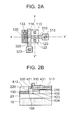
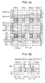
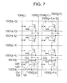
- Fig. 5A shows two cells in the word direction and four cells in the bit direction, eight cells in total (a cell 1000 (j, k), ⁇ , a cell 1000 (j + 1, k + 3)).
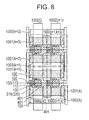
- the mirror image arrangement of cells is also employed in an embodiment of Fig. 8 which will be described later.
- an insulating film for dividing the silicon thin film in the planar direction is called an insulating separation film 401.
- insulating film side walls 403 each having a thickness of about 30 nm are formed on the side faces of the first and second conductive gates.
- the side walls are a two-layer laminate consisting of a silicon nitride film 404 with a thickness of about 7 nm and a silicon oxide film 405 with a thickness of about 23 nm. At this stage, the silicon nitride film 404 is left on the semiconductor thin film.
- the silicon nitride film 43 on the conductive gate thin film (300) is subjected to wet etching by hot phosphoric acid or the like. The surface is then rinsed, nickel is deposited by evaporation to a thickness of about 20 nm, and next follows sintering. The nickel on the insulating film that has not reacted is etched by an acid to leave a nickel silicide layer.
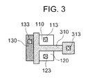
- a silicide layer 110s is formed on the first semiconductor region (drain)
- a silicide layer 120s is formed on the second semiconductor region (source)
- a silicide layer 300s is formed on the gate thin film.
- the features of this embodiment are (1) that the third semiconductor region and the first semiconductor region are insulated by the insulating film 406 formed on the side face of the crystal thin film that is obtained by selective epitaxial growth and (2) that the gate threshold voltage for inducing carriers of the opposite type differs between in the first channel formation semiconductor thin film portion and in the opposite conductivity type carrier channel which leads to the first channel formation semiconductor thin film portion from the third semiconductor region.
- the third semiconductor region and the first semiconductor region are connected to the same bit line (one bit line doubles as a writing bit line and a reading bit line different from the case in the memory array of Figs. 5A and 5B ).
Landscapes
- Engineering & Computer Science (AREA)
- Manufacturing & Machinery (AREA)
- Semiconductor Memories (AREA)
- Non-Volatile Memory (AREA)
- Dram (AREA)
- Read Only Memory (AREA)
Applications Claiming Priority (4)
| Application Number | Priority Date | Filing Date | Title |
|---|---|---|---|
| JP2002108423 | 2002-04-10 | ||
| JP2002230397 | 2002-08-07 | ||
| JP2003086898A JP4880867B2 (ja) | 2002-04-10 | 2003-03-27 | 薄膜メモリ、アレイとその動作方法および製造方法 |
| EP03252253A EP1355358B1 (de) | 2002-04-10 | 2003-04-09 | Dünnschicht-Halbleiterspeicher und Verfahren zu seiner Herstellung |
Related Parent Applications (2)
| Application Number | Title | Priority Date | Filing Date |
|---|---|---|---|
| EP03252253.4 Division | 2003-04-09 | ||
| EP03252253A Division EP1355358B1 (de) | 2002-04-10 | 2003-04-09 | Dünnschicht-Halbleiterspeicher und Verfahren zu seiner Herstellung |
Publications (3)
| Publication Number | Publication Date |
|---|---|
| EP2113943A2 true EP2113943A2 (de) | 2009-11-04 |
| EP2113943A3 EP2113943A3 (de) | 2010-10-13 |
| EP2113943B1 EP2113943B1 (de) | 2013-07-31 |
Family
ID=28678744
Family Applications (2)
| Application Number | Title | Priority Date | Filing Date |
|---|---|---|---|
| EP03252253A Expired - Lifetime EP1355358B1 (de) | 2002-04-10 | 2003-04-09 | Dünnschicht-Halbleiterspeicher und Verfahren zu seiner Herstellung |
| EP09166746.9A Expired - Lifetime EP2113943B1 (de) | 2002-04-10 | 2003-04-09 | Dünnschichtspeicher, Array, und Betriebs- und Herstellungsmethode dafür |
Family Applications Before (1)
| Application Number | Title | Priority Date | Filing Date |
|---|---|---|---|
| EP03252253A Expired - Lifetime EP1355358B1 (de) | 2002-04-10 | 2003-04-09 | Dünnschicht-Halbleiterspeicher und Verfahren zu seiner Herstellung |
Country Status (6)
| Country | Link |
|---|---|
| US (2) | US20030213994A1 (de) |
| EP (2) | EP1355358B1 (de) |
| JP (1) | JP4880867B2 (de) |
| KR (1) | KR100983408B1 (de) |
| CN (1) | CN100380666C (de) |
| TW (1) | TWI264116B (de) |
Cited By (4)
| Publication number | Priority date | Publication date | Assignee | Title |
|---|---|---|---|---|
| US8354660B2 (en) | 2010-03-16 | 2013-01-15 | Sandisk 3D Llc | Bottom electrodes for use with metal oxide resistivity switching layers |
| US8389971B2 (en) | 2010-10-14 | 2013-03-05 | Sandisk 3D Llc | Memory cells having storage elements that share material layers with steering elements and methods of forming the same |
| US8841648B2 (en) | 2010-10-14 | 2014-09-23 | Sandisk 3D Llc | Multi-level memory arrays with memory cells that employ bipolar storage elements and methods of forming the same |
| US10797054B2 (en) | 2009-12-28 | 2020-10-06 | Semiconductor Energy Laboratory Co., Ltd. | Memory device and semiconductor device |
Families Citing this family (65)
| Publication number | Priority date | Publication date | Assignee | Title |
|---|---|---|---|---|
| EP1355316B1 (de) | 2002-04-18 | 2007-02-21 | Innovative Silicon SA | Datenspeichergerät sowie Verfahren zum Auffrischen der auf einem solchen Gerät gespeicherten Daten |
| EP1357603A3 (de) | 2002-04-18 | 2004-01-14 | Innovative Silicon SA | Halbleiterbauelement |
| US6912150B2 (en) | 2003-05-13 | 2005-06-28 | Lionel Portman | Reference current generator, and method of programming, adjusting and/or operating same |
| US7085153B2 (en) | 2003-05-13 | 2006-08-01 | Innovative Silicon S.A. | Semiconductor memory cell, array, architecture and device, and method of operating same |
| US20040228168A1 (en) | 2003-05-13 | 2004-11-18 | Richard Ferrant | Semiconductor memory device and method of operating same |
| US7335934B2 (en) | 2003-07-22 | 2008-02-26 | Innovative Silicon S.A. | Integrated circuit device, and method of fabricating same |
| US7184298B2 (en) | 2003-09-24 | 2007-02-27 | Innovative Silicon S.A. | Low power programming technique for a floating body memory transistor, memory cell, and memory array |
| US7301803B2 (en) * | 2004-12-22 | 2007-11-27 | Innovative Silicon S.A. | Bipolar reading technique for a memory cell having an electrically floating body transistor |
| FR2880710B1 (fr) * | 2005-01-11 | 2007-04-20 | St Microelectronics Sa | Procede et dispositif de caracterisation d'une cellule destinee a etre realisee dans une technologie cmos du type silicium sur isolant partiellement appauvri |
| KR100673228B1 (ko) * | 2005-06-30 | 2007-01-22 | 주식회사 하이닉스반도체 | 낸드 플래쉬 메모리 소자의 제조방법 |
| US20070023833A1 (en) * | 2005-07-28 | 2007-02-01 | Serguei Okhonin | Method for reading a memory cell having an electrically floating body transistor, and memory cell and array implementing same |
| US7606066B2 (en) | 2005-09-07 | 2009-10-20 | Innovative Silicon Isi Sa | Memory cell and memory cell array having an electrically floating body transistor, and methods of operating same |
| US7683430B2 (en) * | 2005-12-19 | 2010-03-23 | Innovative Silicon Isi Sa | Electrically floating body memory cell and array, and method of operating or controlling same |
| US7542345B2 (en) * | 2006-02-16 | 2009-06-02 | Innovative Silicon Isi Sa | Multi-bit memory cell having electrically floating body transistor, and method of programming and reading same |
| US7492632B2 (en) | 2006-04-07 | 2009-02-17 | Innovative Silicon Isi Sa | Memory array having a programmable word length, and method of operating same |
| US7606098B2 (en) | 2006-04-18 | 2009-10-20 | Innovative Silicon Isi Sa | Semiconductor memory array architecture with grouped memory cells, and method of controlling same |
| US7933142B2 (en) | 2006-05-02 | 2011-04-26 | Micron Technology, Inc. | Semiconductor memory cell and array using punch-through to program and read same |
| US8069377B2 (en) | 2006-06-26 | 2011-11-29 | Micron Technology, Inc. | Integrated circuit having memory array including ECC and column redundancy and method of operating the same |
| US7542340B2 (en) * | 2006-07-11 | 2009-06-02 | Innovative Silicon Isi Sa | Integrated circuit including memory array having a segmented bit line architecture and method of controlling and/or operating same |
| US7893475B2 (en) * | 2007-01-24 | 2011-02-22 | Macronix International Co., Ltd. | Dynamic random access memory cell and manufacturing method thereof |
| KR101406604B1 (ko) | 2007-01-26 | 2014-06-11 | 마이크론 테크놀로지, 인코포레이티드 | 게이트형 바디 영역으로부터 격리되는 소스/드레인 영역을 포함하는 플로팅-바디 dram 트랜지스터 |
| US7919800B2 (en) | 2007-02-26 | 2011-04-05 | Micron Technology, Inc. | Capacitor-less memory cells and cell arrays |
| US8518774B2 (en) * | 2007-03-29 | 2013-08-27 | Micron Technology, Inc. | Manufacturing process for zero-capacitor random access memory circuits |
| US8064274B2 (en) | 2007-05-30 | 2011-11-22 | Micron Technology, Inc. | Integrated circuit having voltage generation circuitry for memory cell array, and method of operating and/or controlling same |
| US8085594B2 (en) | 2007-06-01 | 2011-12-27 | Micron Technology, Inc. | Reading technique for memory cell with electrically floating body transistor |
| US8194487B2 (en) | 2007-09-17 | 2012-06-05 | Micron Technology, Inc. | Refreshing data of memory cells with electrically floating body transistors |
| JP2009088440A (ja) * | 2007-10-03 | 2009-04-23 | Oki Semiconductor Co Ltd | 半導体装置及びその製造方法 |
| US8536628B2 (en) | 2007-11-29 | 2013-09-17 | Micron Technology, Inc. | Integrated circuit having memory cell array including barriers, and method of manufacturing same |
| US8349662B2 (en) * | 2007-12-11 | 2013-01-08 | Micron Technology, Inc. | Integrated circuit having memory cell array, and method of manufacturing same |
| JP2009169071A (ja) * | 2008-01-16 | 2009-07-30 | Sony Corp | 表示装置 |
| US8773933B2 (en) | 2012-03-16 | 2014-07-08 | Micron Technology, Inc. | Techniques for accessing memory cells |
| US8014195B2 (en) | 2008-02-06 | 2011-09-06 | Micron Technology, Inc. | Single transistor memory cell |
| US8189376B2 (en) * | 2008-02-08 | 2012-05-29 | Micron Technology, Inc. | Integrated circuit having memory cells including gate material having high work function, and method of manufacturing same |
| US7957206B2 (en) * | 2008-04-04 | 2011-06-07 | Micron Technology, Inc. | Read circuitry for an integrated circuit having memory cells and/or a memory cell array, and method of operating same |
| KR101505494B1 (ko) | 2008-04-30 | 2015-03-24 | 한양대학교 산학협력단 | 무 커패시터 메모리 소자 |
| US7947543B2 (en) | 2008-09-25 | 2011-05-24 | Micron Technology, Inc. | Recessed gate silicon-on-insulator floating body device with self-aligned lateral isolation |
| US7933140B2 (en) | 2008-10-02 | 2011-04-26 | Micron Technology, Inc. | Techniques for reducing a voltage swing |
| US7924630B2 (en) * | 2008-10-15 | 2011-04-12 | Micron Technology, Inc. | Techniques for simultaneously driving a plurality of source lines |
| US8223574B2 (en) * | 2008-11-05 | 2012-07-17 | Micron Technology, Inc. | Techniques for block refreshing a semiconductor memory device |
| KR101570178B1 (ko) * | 2008-11-07 | 2015-11-18 | 삼성전자주식회사 | 커패시터 없는 디램 소자 |
| US8213226B2 (en) * | 2008-12-05 | 2012-07-03 | Micron Technology, Inc. | Vertical transistor memory cell and array |
| US8278167B2 (en) | 2008-12-18 | 2012-10-02 | Micron Technology, Inc. | Method and structure for integrating capacitor-less memory cell with logic |
| US8319294B2 (en) * | 2009-02-18 | 2012-11-27 | Micron Technology, Inc. | Techniques for providing a source line plane |
| WO2010102106A2 (en) | 2009-03-04 | 2010-09-10 | Innovative Silicon Isi Sa | Techniques for forming a contact to a buried diffusion layer in a semiconductor memory device |
| CN102365628B (zh) | 2009-03-31 | 2015-05-20 | 美光科技公司 | 用于提供半导体存储器装置的技术 |
| US8139418B2 (en) | 2009-04-27 | 2012-03-20 | Micron Technology, Inc. | Techniques for controlling a direct injection semiconductor memory device |
| US8508994B2 (en) * | 2009-04-30 | 2013-08-13 | Micron Technology, Inc. | Semiconductor device with floating gate and electrically floating body |
| US8498157B2 (en) * | 2009-05-22 | 2013-07-30 | Micron Technology, Inc. | Techniques for providing a direct injection semiconductor memory device |
| US8537610B2 (en) | 2009-07-10 | 2013-09-17 | Micron Technology, Inc. | Techniques for providing a semiconductor memory device |
| US9076543B2 (en) | 2009-07-27 | 2015-07-07 | Micron Technology, Inc. | Techniques for providing a direct injection semiconductor memory device |
| US8199595B2 (en) * | 2009-09-04 | 2012-06-12 | Micron Technology, Inc. | Techniques for sensing a semiconductor memory device |
| US8174881B2 (en) | 2009-11-24 | 2012-05-08 | Micron Technology, Inc. | Techniques for reducing disturbance in a semiconductor device |
| US8310893B2 (en) * | 2009-12-16 | 2012-11-13 | Micron Technology, Inc. | Techniques for reducing impact of array disturbs in a semiconductor memory device |
| US8416636B2 (en) | 2010-02-12 | 2013-04-09 | Micron Technology, Inc. | Techniques for controlling a semiconductor memory device |
| US8576631B2 (en) | 2010-03-04 | 2013-11-05 | Micron Technology, Inc. | Techniques for sensing a semiconductor memory device |
| US8411513B2 (en) * | 2010-03-04 | 2013-04-02 | Micron Technology, Inc. | Techniques for providing a semiconductor memory device having hierarchical bit lines |
| US8369177B2 (en) * | 2010-03-05 | 2013-02-05 | Micron Technology, Inc. | Techniques for reading from and/or writing to a semiconductor memory device |
| CN102812552B (zh) | 2010-03-15 | 2015-11-25 | 美光科技公司 | 半导体存储器装置及用于对半导体存储器装置进行偏置的方法 |
| US8411524B2 (en) | 2010-05-06 | 2013-04-02 | Micron Technology, Inc. | Techniques for refreshing a semiconductor memory device |
| US8531878B2 (en) | 2011-05-17 | 2013-09-10 | Micron Technology, Inc. | Techniques for providing a semiconductor memory device |
| US9559216B2 (en) | 2011-06-06 | 2017-01-31 | Micron Technology, Inc. | Semiconductor memory device and method for biasing same |
| WO2015085093A1 (en) | 2013-12-06 | 2015-06-11 | Rambus Inc. | 2t-1r architecture for resistive ram |
| CN109643639B (zh) * | 2016-09-13 | 2023-08-11 | 应用材料公司 | 用于间隔件和硬掩模应用的硼烷介导的从硅烷和烷基硅烷物质脱氢的工艺 |
| US11088140B2 (en) * | 2019-08-27 | 2021-08-10 | Nanya Technology Corporation | Multiple semiconductor elements with different threshold voltages |
| US11821936B2 (en) * | 2022-01-10 | 2023-11-21 | Nxp Usa, Inc. | In situ threshold voltage determination of a semiconductor device |
Family Cites Families (15)
| Publication number | Priority date | Publication date | Assignee | Title |
|---|---|---|---|---|
| US4118693A (en) * | 1977-05-09 | 1978-10-03 | Knogo Corporation | Method and apparatus for producing uniform electromagnetic fields in an article detection system |
| JPS586234B2 (ja) * | 1977-11-17 | 1983-02-03 | 富士通株式会社 | 半導体記憶装置 |
| JPS5893370A (ja) * | 1981-11-30 | 1983-06-03 | Nec Corp | Mosデバイス |
| JPS6235559A (ja) * | 1985-08-09 | 1987-02-16 | Agency Of Ind Science & Technol | 半導体記憶装置 |
| US5283457A (en) * | 1989-10-02 | 1994-02-01 | Texas Instruments Incorporated | Semiconductor on insulator transistor |
| JPH0799251A (ja) * | 1992-12-10 | 1995-04-11 | Sony Corp | 半導体メモリセル |
| GB9401924D0 (en) * | 1994-02-01 | 1994-03-30 | Jonhig Ltd | System for road toll payment |
| US5784311A (en) * | 1997-06-13 | 1998-07-21 | International Business Machines Corporation | Two-device memory cell on SOI for merged logic and memory applications |
| JPH11224906A (ja) * | 1998-02-05 | 1999-08-17 | Sony Corp | 半導体メモリセル |
| US6225665B1 (en) * | 1999-01-11 | 2001-05-01 | Mitsubishi Denki Kabushiki Kaisha | Semiconductor device having multiple source regions |
| US6111778A (en) * | 1999-05-10 | 2000-08-29 | International Business Machines Corporation | Body contacted dynamic memory |
| TW557569B (en) * | 2000-01-24 | 2003-10-11 | Sony Corp | Semiconductor device and manufacturing method thereof |
| JP3485091B2 (ja) * | 2001-01-19 | 2004-01-13 | セイコーエプソン株式会社 | 半導体装置およびその製造方法 |
| US6793127B2 (en) * | 2001-04-04 | 2004-09-21 | Koninklijke Philips Electronics N.V. | Internet enabled resource constrained terminal for processing tags |
| US8321302B2 (en) * | 2002-01-23 | 2012-11-27 | Sensormatic Electronics, LLC | Inventory management system |
-
2003
- 2003-03-27 JP JP2003086898A patent/JP4880867B2/ja not_active Expired - Fee Related
- 2003-04-04 TW TW092107778A patent/TWI264116B/zh not_active IP Right Cessation
- 2003-04-09 EP EP03252253A patent/EP1355358B1/de not_active Expired - Lifetime
- 2003-04-09 US US10/410,239 patent/US20030213994A1/en not_active Abandoned
- 2003-04-09 EP EP09166746.9A patent/EP2113943B1/de not_active Expired - Lifetime
- 2003-04-10 KR KR1020030022660A patent/KR100983408B1/ko not_active Expired - Fee Related
- 2003-04-10 CN CNB031307892A patent/CN100380666C/zh not_active Expired - Fee Related
-
2004
- 2004-06-28 US US10/879,938 patent/US7211867B2/en not_active Expired - Lifetime
Non-Patent Citations (2)
| Title |
|---|
| H. J. WANN; C. HU: "A capacitor-less DRAM cell on SOl substrate", IEDM (INTERNATIONAL ELECTRON DEVICE MEETING) TECHNICAL DIGEST, 1993, pages 635 - 638 |
| S. OKHONIN ET AL.: "A Capacitor-less lT-DRAM Cell", IEEE ELECTRON DEVICE LETTERS, vol. 23, no. 2, February 2002 (2002-02-01), pages 85 - 87 |
Cited By (10)
| Publication number | Priority date | Publication date | Assignee | Title |
|---|---|---|---|---|
| US10797054B2 (en) | 2009-12-28 | 2020-10-06 | Semiconductor Energy Laboratory Co., Ltd. | Memory device and semiconductor device |
| US11424246B2 (en) | 2009-12-28 | 2022-08-23 | Semiconductor Energy Laboratory Co., Ltd. | Memory device and semiconductor device |
| US12193244B2 (en) | 2009-12-28 | 2025-01-07 | Semiconductor Energy Laboratory Co., Ltd. | Memory device and semiconductor device |
| US8354660B2 (en) | 2010-03-16 | 2013-01-15 | Sandisk 3D Llc | Bottom electrodes for use with metal oxide resistivity switching layers |
| US8772749B2 (en) | 2010-03-16 | 2014-07-08 | Sandisk 3D Llc | Bottom electrodes for use with metal oxide resistivity switching layers |
| US8389971B2 (en) | 2010-10-14 | 2013-03-05 | Sandisk 3D Llc | Memory cells having storage elements that share material layers with steering elements and methods of forming the same |
| US8841648B2 (en) | 2010-10-14 | 2014-09-23 | Sandisk 3D Llc | Multi-level memory arrays with memory cells that employ bipolar storage elements and methods of forming the same |
| US8969845B2 (en) | 2010-10-14 | 2015-03-03 | Sandisk 3D Llc | Memory cells having storage elements that share material layers with steering elements and methods of forming the same |
| US8981331B2 (en) | 2010-10-14 | 2015-03-17 | Sandisk 3D Llc | Memory cells having storage elements that share material layers with steering elements and methods of forming the same |
| US9105576B2 (en) | 2010-10-14 | 2015-08-11 | Sandisk 3D Llc | Multi-level memory arrays with memory cells that employ bipolar storage elements and methods of forming the same |
Also Published As
| Publication number | Publication date |
|---|---|
| TW200308082A (en) | 2003-12-16 |
| CN1453874A (zh) | 2003-11-05 |
| EP2113943B1 (de) | 2013-07-31 |
| KR20030081142A (ko) | 2003-10-17 |
| JP4880867B2 (ja) | 2012-02-22 |
| US20050001269A1 (en) | 2005-01-06 |
| EP1355358A3 (de) | 2004-08-04 |
| KR100983408B1 (ko) | 2010-09-20 |
| EP1355358A2 (de) | 2003-10-22 |
| US20030213994A1 (en) | 2003-11-20 |
| US7211867B2 (en) | 2007-05-01 |
| JP2004128446A (ja) | 2004-04-22 |
| EP2113943A3 (de) | 2010-10-13 |
| CN100380666C (zh) | 2008-04-09 |
| EP1355358B1 (de) | 2013-03-13 |
| TWI264116B (en) | 2006-10-11 |
Similar Documents
| Publication | Publication Date | Title |
|---|---|---|
| EP1355358B1 (de) | Dünnschicht-Halbleiterspeicher und Verfahren zu seiner Herstellung | |
| JP4927321B2 (ja) | 半導体記憶装置 | |
| US6559012B2 (en) | Method for manufacturing semiconductor integrated circuit device having floating gate and deposited film | |
| US5466961A (en) | Semiconductor device and method of manufacturing the same | |
| US6864136B2 (en) | DRAM cell with enhanced SER immunity | |
| US6787411B2 (en) | Method of manufacturing semiconductor memory device and semiconductor memory device | |
| US8143656B2 (en) | High performance one-transistor DRAM cell device and manufacturing method thereof | |
| US8361863B2 (en) | Embedded DRAM with multiple gate oxide thicknesses | |
| US7265419B2 (en) | Semiconductor memory device with cell transistors having electrically floating channel bodies to store data | |
| JPH05136374A (ja) | 半導体装置及びその製造方法 | |
| US7244977B2 (en) | Longitudinal MISFET manufacturing method, longitudinal MISFET, semiconductor storage device manufacturing method, and semiconductor storage device | |
| US6924237B2 (en) | Method for manufacturing semiconductor integrated circuit device | |
| JP2003303901A (ja) | 半導体集積回路装置およびその製造方法 | |
| US4989056A (en) | Semiconductor capacitor | |
| US20040232464A1 (en) | Semiconductor integrated circuit device and manufacturing method thereof | |
| US7929359B2 (en) | Embedded DRAM with bias-independent capacitance | |
| JP2001267531A (ja) | 半導体集積回路装置 | |
| JP2003209189A (ja) | 半導体集積回路装置およびその製造方法 |
Legal Events
| Date | Code | Title | Description |
|---|---|---|---|
| PUAI | Public reference made under article 153(3) epc to a published international application that has entered the european phase |
Free format text: ORIGINAL CODE: 0009012 |
|
| 17P | Request for examination filed |
Effective date: 20090825 |
|
| AC | Divisional application: reference to earlier application |
Ref document number: 1355358 Country of ref document: EP Kind code of ref document: P |
|
| AK | Designated contracting states |
Kind code of ref document: A2 Designated state(s): FR NL |
|
| R17P | Request for examination filed (corrected) |
Effective date: 20090825 |
|
| PUAL | Search report despatched |
Free format text: ORIGINAL CODE: 0009013 |
|
| AK | Designated contracting states |
Kind code of ref document: A3 Designated state(s): FR NL |
|
| RIC1 | Information provided on ipc code assigned before grant |
Ipc: H01L 21/84 20060101ALI20100909BHEP Ipc: H01L 27/12 20060101ALI20100909BHEP Ipc: H01L 27/108 20060101AFI20090925BHEP Ipc: H01L 21/8242 20060101ALI20100909BHEP |
|
| 17Q | First examination report despatched |
Effective date: 20120309 |
|
| GRAP | Despatch of communication of intention to grant a patent |
Free format text: ORIGINAL CODE: EPIDOSNIGR1 |
|
| GRAS | Grant fee paid |
Free format text: ORIGINAL CODE: EPIDOSNIGR3 |
|
| GRAA | (expected) grant |
Free format text: ORIGINAL CODE: 0009210 |
|
| AC | Divisional application: reference to earlier application |
Ref document number: 1355358 Country of ref document: EP Kind code of ref document: P |
|
| AK | Designated contracting states |
Kind code of ref document: B1 Designated state(s): FR NL |
|
| REG | Reference to a national code |
Ref country code: NL Ref legal event code: T3 |
|
| PLBE | No opposition filed within time limit |
Free format text: ORIGINAL CODE: 0009261 |
|
| STAA | Information on the status of an ep patent application or granted ep patent |
Free format text: STATUS: NO OPPOSITION FILED WITHIN TIME LIMIT |
|
| 26N | No opposition filed |
Effective date: 20140502 |
|
| REG | Reference to a national code |
Ref country code: FR Ref legal event code: PLFP Year of fee payment: 14 |
|
| REG | Reference to a national code |
Ref country code: NL Ref legal event code: PD Owner name: SII SEMICONDUCTOR CORPORATION; JP Free format text: DETAILS ASSIGNMENT: VERANDERING VAN EIGENAAR(S), OVERDRACHT; FORMER OWNER NAME: SEIKO INSTRUMENTS INC. Effective date: 20160315 |
|
| REG | Reference to a national code |
Ref country code: FR Ref legal event code: TQ Owner name: HAYASHI, YUTAKA, JP Effective date: 20160905 Ref country code: FR Ref legal event code: TQ Owner name: SII SEMICONDUCTOR CORPORATION, JP Effective date: 20160905 |
|
| REG | Reference to a national code |
Ref country code: FR Ref legal event code: PLFP Year of fee payment: 15 |
|
| REG | Reference to a national code |
Ref country code: FR Ref legal event code: PLFP Year of fee payment: 16 |
|
| REG | Reference to a national code |
Ref country code: NL Ref legal event code: HC Owner name: ABLIC INC.; JP Free format text: DETAILS ASSIGNMENT: CHANGE OF OWNER(S), CHANGE OF OWNER(S) NAME; FORMER OWNER NAME: SII SEMICONDUCTOR CORPORATION Effective date: 20180810 |
|
| PGFP | Annual fee paid to national office [announced via postgrant information from national office to epo] |
Ref country code: NL Payment date: 20200312 Year of fee payment: 18 |
|
| PGFP | Annual fee paid to national office [announced via postgrant information from national office to epo] |
Ref country code: FR Payment date: 20200312 Year of fee payment: 18 |
|
| REG | Reference to a national code |
Ref country code: NL Ref legal event code: MM Effective date: 20210501 |
|
| PG25 | Lapsed in a contracting state [announced via postgrant information from national office to epo] |
Ref country code: FR Free format text: LAPSE BECAUSE OF NON-PAYMENT OF DUE FEES Effective date: 20210430 |
|
| PG25 | Lapsed in a contracting state [announced via postgrant information from national office to epo] |
Ref country code: NL Free format text: LAPSE BECAUSE OF NON-PAYMENT OF DUE FEES Effective date: 20210501 |